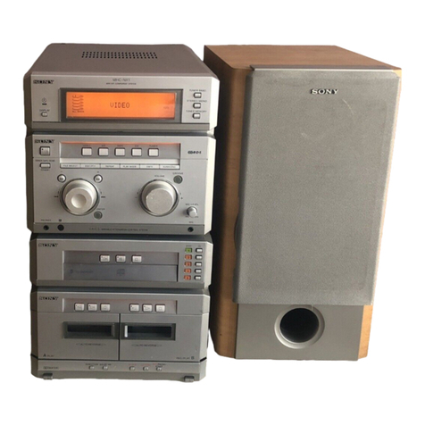
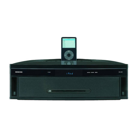
Sony HCD-EH15 User manual

SERVICE MANUAL
Sony Corporation
Audio Business Group
Published by Sony Techno Create Corporation
HCD-EH15
SPECIFICATIONS
COMPACT DISC DECK RECEIVER
9-889-094-01
2008D05-1
© 2008.04
Canadian Model
UK Model
E Model
Australian Model
Russian Model
Ver. 1.0 2008.04
• HCD-EH15 is the amplifier, CD player, tape
deck and tuner section in CMT-EH15.
CD
Section
Model Name Using Similar Mechanism NEW
Base Unit Name BU-K8BD90-WOD
Optical Pick-up Name KSM-213CDP
Tape
Section
Model Name Using Similar Mechanism NEW
Tape Transport Mechanism Type MF-EH10
Amplifier section
European and Russian models:
DIN power output (rated): 4 + 4 W (4 ohms at 1 kHz, DIN)
Continuous RMS power output (reference): 5 + 5 W (4 ohms at 1 kHz,
10% THD)
Music power output (reference): 7 + 7 W
Other models:
DIN power output (rated): 4 + 4 W (4 ohms at 1 kHz, DIN)
Continuous RMS power output (reference): 5 + 5 W (4 ohms at 1 kHz,
10% THD)
Inputs
AUDIO IN (stereo mini jack): Sensitivity 800 mV, impedance 47 kilohms
Outputs
PHONES (stereo mini jack): Accepts headphones with an impedance of
8 ohms or more
SPEAKER: Accepts impedance of 4 ohms
CD player section
System: Compact disc and digital audio system
Laser Diode Properties
Emission Duration: Continuous
Laser Output*: Less than 44.6μW
* is output is the value measurement at a distance of 200 mm from the
objective lens surface on the Optical Pick-up Block with 7 mm aperture.
Frequency response: 20 Hz 20 kHz
Signal-to-noise ratio: More than 90 dB
Dynamic range: More than 90 dB
Tape deck section
Recording system: 4-track 2-channel, stereo
Tuner section
FM stereo, FM/AM superheterodyne tuner
Antenna:
FM lead antenna
AM loop antenna
FM tuner section:
Tuning range
Canadian model: 87.5 108.0 MHz (100 kHz step)
Other models: 87.5 108.0 MHz (50 kHz step)
Intermediate frequency: 10.7 MHz
AM tuner section:
Tuning range
Canadian and Latin American models:
530 1,710 kHz (with 10 kHz tuning interval)
531 1,710 kHz (with 9 kHz tuning interval)
European and Russian models:
531 1,602 kHz (with 9 kHz tuning interval)
Australian model:
531 1,710 kHz (with 9 kHz tuning interval)
530 1,710 kHz (with 10 kHz tuning interval)
Other models:
531 1,602 kHz (with 9 kHz tuning interval)
530 1,610 kHz (with 10 kHz tuning interval)
Intermediate frequency: 450 kHz
General
Power requirements:
Canadian model: AC 120 V, 60 Hz
Eu
Mexican model: AC 120 V, 60 Hz
ropean and Russian models: AC 230 V, 50/60 Hz
Australian model: AC 230 240 V, 50/60 Hz
Argentine model: AC 220 V, 50/60 Hz
Korean model: AC 220 V, 60 Hz
Taiwan model: AC 120 V, 50/60 Hz
Other models: AC 110 120 or 220 240 V, 50/60 Hz
Adjustable with voltage selector
Power consumption: 25 W
Dimensions (w/h/d) (excl. speakers): Approx. 155 × 241 × 224.6 mm
Mass (excl. speakers): Approx. 2.2 kg
Design and specications are subject to change without notice.

HCD-EH15
2
1. SERVICING NOTES ............................................. 3
2. GENERAL .................................................................. 4
3. DISASSEMBLY
3-1. Disassembly Flow........................................................... 6
3-2. Rear Cabinet Block......................................................... 6
3-3. Front Cabinet Block, Top Cabinet Block,
MAIN Board ................................................................... 7
3-4. MF-EH10 (Tape Mechanism Deck), Cassette Lid.......... 7
3-5. Base Unit Block (BU-K8BD90-WOD) .......................... 8
3-6. Optical Pick-up Block (KSM-213CDP) ......................... 8
4. TEST MODE ............................................................ 9
5. MECHANICAL ADJUSTMENTS ...................... 10
6. ELECTRICAL ADJUSTMENTS ........................ 10
7. DIAGRAMS
7-1. Printed Wiring Board - CD Board - ................................ 14
7-2. Schematic Diagram - CD Board -................................... 15
7-3. Printed Wiring Board - PANEL Board - ......................... 16
7-4. Schematic Diagram - PANEL Board -............................ 17
7-5. Schematic Diagram - MAIN Section (1/2) -................... 18
7-6. Schematic Diagram - MAIN Section (2/2) -................... 19
7-7. Printed Wiring Boards - MAIN Section - ....................... 20
8. EXPLODED VIEWS
8-1. Overall Section ............................................................... 27
8-2. Front Cabinet Section ..................................................... 28
8-3. Top Cabinet Section........................................................ 29
8-4. Base Unit Section (BU-K8BD90-WOD)........................ 30
9. ELECTRICAL PARTS LIST .............................. 31
TABLE OF CONTENTSNotes on chip component replacement
• Never reuse a disconnected chip component.
• Notice that the minus side of a tantalum capacitor may be dam-
aged by heat.
SAFETY-RELATED COMPONET WARNING!
COMPONENTS IDENTIFIED BY MARK 0OR DOTTED LINE
WITH MARK 0ON THE SCHEMATIC DIAGRAMS AND IN
THE PARTS LIST ARE CRITICAL TO SAFE OPERATION.
REPLACE THESE COMPONENTS WITH SONY PARTS
WHOSE PART NUMBERS APPEAR AS SHOWN IN THIS
MANUAL OR IN SUPPLEMENTS PUBLISHED BY SONY.
ATTENTION AU COMPOSANT AYANT RAPPORT
À LA SÉCURITÉ!
LES COMPOSANTS IDENTIFIÉS PAR UNE MARQUE 0SUR
LES DIAGRAMMES SCHÉMATIQUES ET LA LISTE DES
PIÈCES SONT CRITIQUES POUR LA SÉCURITÉ DE FONC-
TIONNEMENT. NE REMPLACER CES COM- POSANTS QUE
PAR DES PIÈCES SONY DONT LES NUMÉROS SONT DON-
NÉS DANS CE MANUEL OU DANS LES SUPPLÉMENTS
PUBLIÉS PAR SONY.
is appliance is classied
as a CLASS 1 LASER
product. is marking
is located on the rear
exterior.
CAUTION
Use of controls or adjustments or performance of procedures other than
those specified herein may result in hazardous radiation exposure.

HCD-EH15
3
SECTION 1
SERVICING NOTES
UNLEADED SOLDER
Boards requiring use of unleaded solder are printed with the lead-
free mark (LF) indicating the solder contains no lead.
(Caution: Some printed circuit boards may not come printed with
the lead free mark due to their particular size)
: LEAD FREE MARK
Unleaded solder has the following characteristics.
• Unleaded solder melts at a temperature about 40 °C higher
than ordinary solder.
Ordinary soldering irons can be used but the iron tip has to be
applied to the solder joint for a slightly longer time.
Soldering irons using a temperature regulator should be set to
about 350 °C.
Caution: The printed pattern (copper foil) may peel away if the
heated tip is applied for too long, so be careful!
• Strong viscosity
Unleaded solder is more viscous (sticky, less prone to flow)
than ordinary solder so use caution not to let solder bridges
occur such as on IC pins, etc.
• Usable with ordinary solder
It is best to use only unleaded solder but unleaded solder may
also be added to ordinary solder.
NOTES ON HANDLING THE OPTICAL PICK-UP
BLOCK OR BASE UNIT
The laser diode in the optical pick-up block may suffer electrostat-
ic break-down because of the potential difference generated by the
charged electrostatic load, etc. on clothing and the human body.
During repair, pay attention to electrostatic break-down and also
use the procedure in the printed matter which is included in the
repair parts.
The flexible board is easily damaged and should be handled with
care.
NOTES ON LASER DIODE EMISSION CHECK
The laser beam on this model is concentrated so as to be focused
on the disc reflective surface by the objective lens in the optical
pickup block. Therefore, when checking the laser diode emission,
observe from more than 30 cm away from the objective lens.
LASER DIODE AND FOCUS SEARCH OPERATION
CHECK
During normal operation of the equipment, emission of the laser
diode is prohibited unless the upper lid is closed while turning on
the SW750. (push switch type)
The following checking method for the laser diode is operable.
• Method
Emission of the laser diode is visually checked.
1. Open the upper lid.
2. Push the SW750 as shown in Fig.1.
Note: Do not push the detection lever strongly, or it may be bent or
damaged.
3. Check the object lens for confirming normal emission of the
laser diode. If not emitting, there is a trouble in the automatic
power control circuit or the optical pick-up.
In this operation, the object lens will move up and down 2
times along with inward motion for the focus search.
SW750
Fig.1 Method to push the SW750
MODEL IDENTIFICATION
Power Voltage
Indication
–
Rear Cabinet –
Model POWER VOLTAGE INDICATION
Canadian and Mexican
models
AC 120 V, 60 Hz
UK and Russian models AC 230 V, 50/60 Hz
Australian model AC 230 – 240 V, 50/60 Hz
Argentina model AC 220 V, 50/60 Hz
Korean model AC 220 V, 60 Hz
Taiwan model AC 120 V, 50/60 Hz
Singapore, Chilean and
Peruvian models
AC 110 – 120 or 220 – 240 V,
50/60 Hz

HCD-EH15
4
SECTION 2
GENERAL This section is extracted
from instruction manual.
Basic Operations
Open the tape
section lid.
is manual mainly explains operations using the
remote, but the same operations can also be performed
using the buttons on the unit having the same or similar
names.
Before using the system
To use the remote
Slide and remove the battery compartment lid , and
insert the two R6 (size AA) batteries (not supplied),
side rst, matching the polarities shown below.
Notes on using the remote
With normal use, the batteries should last for about six months.
Do not mix an old battery with a new one or mix dierent types of
batteries.
If you do not use the remote for a long period of time, remove the
batteries to avoid damage from battery leakage and corrosion.
To set the clock
Use buttons on the remote to set the clock.
1Turn on the system.
Press (on/standby) .
2Select the clock set mode.
Press CLOCK/TIMER SET . If the current mode
appears, press /repeatedly to select
“CLOCK,” and then press ENTER .
3Set the time.
Press /repeatedly to set the hour, and
then press ENTER . Use the same procedure to set
the minutes.
e clock settings are lost when you disconnect the
power cord or if a power failure occurs.
Selecting a music source
Press the following buttons (or press FUNCTION
repeatedly).
To select Press
CD CD .
Tuner TUNER/BAND .
Tape FUNCTION
repeatedly until “TAPE”
appears.
Component* (connected
using an audio cord) AUDIO IN .
* If the component has the AVLS (Automatic Volume Limiter System)
or BASS BOOST function, turn o the function to avoid distorted
sound from the speakers.
Adjusting the sound
To adjust the volume
Press VOLUME +/(or turn the VOLUME control on
the unit) .
To add a sound eect
To Press
Generate a more dynamic
sound (Dynamic Sound
Generator X-tra)
DSGX on the unit.
Set the sound eect EQ .
Playing a CD/MP3 disc
1Select the CD function.
Press CD (or FUNCTION repeatedly) .
2Place a disc.
Press PUSH OPEN/CLOSE on the unit, and place a
disc with the label side up on the CD compartment.
To close the CD compartment, press PUSH OPEN/
CLOSE on the unit.
PUSH OPEN/CLOSE
3Start playback.
Press (play) (or CD/(play/pause) on the unit)
.
To Press
Pause playback (pause) (or CD/on the
unit) . To resume play, press
it again.
Stop playback (stop) .
Select a folder on an
MP3 disc +/(select folder) .
Select a track or le /(go back/go forward)
(/on the unit) .
Find a point in a
track or le
Hold down /(rewind/
fast forward) during playback,
and release it at the desired point.
Select Repeat Play REPEAT repeatedly until
“REP” or “REP1” appears.
To change the play mode
Press PLAY MODE repeatedly while the player is
stopped. You can select normal play (“ ” for all MP3
les in the folder on the disc), shue play (“SHUF” or
“SHUF*”), or program play (“PGM”).
* When playing a CD-DA disc, (SHUF) Play performs the same
operation as SHUF Play.
Notes on Repeat Play
All tracks or les on a disc are played repeatedly up to ve times.
“REP1” indicates that a single track or le is repeated until you stop
it.
Notes on playing MP3 discs
Do not save other types of tracks or les or unnecessary folders on a
disc that has MP3 les.
Folders that have no MP3 les are skipped.
MP3 les are played back in the order that they are recorded onto
the disc.
e system can only play MP3 les that have a le extension of
“.MP3”.
If there are les on the disc that have the “.MP3” le extension,
but that are not MP3 les, the unit may produce noise or may
malfunction.
e maximum number of:
folders is 150 (including the root folder).
MP3 les is 255.
MP3 les and folders that can be contained on a single disc is 256.
folder levels (the tree structure of les) is 8.
Compatibility with all MP3 encoding/writing soware, recording
device, and recording media cannot be guaranteed. Incompatible
MP3 discs may produce noise or interrupted audio or may not play
at all.
Notes on playing multisession discs
If the disc begins with a CD-DA (or MP3) session, it is recognized
as a CD-DA (or MP3) disc, and playback continues until another
session is encountered.
A disc with a mixed CD format is recognized as a CD-DA (audio)
disc.
Listening to the radio
1Select “FM” or “AM.”
Press TUNER/BAND repeatedly.
2Select the tuning mode.
Press TUNING MODE repeatedly until “AUTO”
appears.
3Tune in the desired station.
Press +/(or TUNING +/on the unit) .
Scanning stops automatically when a station is tuned
in. When you tune in a station that provides RDS
services, the station name appears.
Tip
To stop automatic scanning, press (stop) .
To tune in a station with a weak signal
Press TUNING MODE repeatedly until “MANUAL”
appears, and then press +/(or TUNING +/on the
unit) repeatedly to tune in the desired station.
To reduce static noise on a weak FM stereo
station
Press FM MODE repeatedly until “MONO” appears
to turn o stereo reception.
Playing a tape
Use buttons on the unit to play a tape.
1Select the tape function.
Press FUNCTION repeatedly.
2Insert a tape.
Press (stop/eject) , and insert the tape into the
cassette holder. Make sure there is no slack in the tape
to avoid damaging the tape or the tape deck.
3Start playback.
Press (play) .
To Press
Pause playback (pause) . To resume play, press
it again.
Stop playback (stop/eject) .
Rewind or fast
forward*
/(rewind/fast forward) .
* Be sure to press (stop/eject) aer the tape has been wound
or rewound to the end.
Note
Do not turn o the system during playback or recording.
Changing the display
To change Press
Information on
the display1)
DISPLAY repeatedly when the
system is on.
Display mode
(Clock)
DISPLAY when the system is
off2). e clock is displayed for eight
seconds.
1) For example, you can view CD/MP3 disc information, such as the
track or le number or folder name during normal play, or the total
play time while the player is stopped.
2) e STANDBY indicator lights up when the system is turned o.
Notes on the display information
e following are not displayed;
total playing time for a CD-DA disc depending on the play mode.
total playing time for an MP3 disc.
remaining playing time for a track and an MP3 le.
e following are not displayed correctly;
elapsed playing time of an MP3 le encoded using VBR (variable
bit rate).
folder and le names that do not follow either ISO9660 Level 1,
Level 2 or Joliet in the expansion format.
e following are displayed;
ID3 tag information for MP3 les when ID3 version 1 and
version 2 tags are used.
up to 15 characters of ID3 tag information using uppercase letters
(A to Z), numbers (0 to 9), and symbols (‘< > * + , – / @ [ \ ] _).
Using optional audio components
To connect an optional headphones
Connect headphones to the PHONES jack on the
unit.
To connect an optional component
Connect additional audio source component to the
AUDIO IN jack on the unit using an audio analog
cord (not supplied). Turn down the volume on the
system, and then select the AUDIO IN function.
HCD-EH15
5
Other Operations
Creating your own CD program
(Program Play)
Use buttons on the remote to create your own program.
1Press CD to select the CD function.
2Press PLAY MODE repeatedly until“PGM” appears
while the player is stopped.
3Press /repeatedly until the desired
track number appears.
When programming MP3 les, press +/
repeatedly to select the desired folder, and then select
the desired le.
Selected track or le number
4Press ENTER to add the track or le to the
program.
5Repeat steps 3 through 4 to program additional
tracks or les, up to a total of 15 tracks or les.
6To play your program of tracks or les, press .
e program remains available until you open the CD
compartment. To play it again, select the CD function,
and then press .
To cancel Program Play, press PLAY MODE
repeatedly until “PGM” disappears while the player is
stopped.
To delete the last track or le of the program, press
CLEAR while the player is stopped.
To view program information, such as total track number
of the program, press DISPLAY repeatedly.
Presetting radio stations
You can preset your favorite radio stations and tune
them in instantly by selecting the corresponding preset
number.
Use buttons on the remote to preset stations.
1Press TUNER/BAND repeatedly to select “FM” or
“AM.”
2Press TUNING MODE repeatedly until “AUTO”
appears (or “MANUAL” appears, for a station with a
weak signal).
3Press +/to tune in the desired station.
Scanning stops automatically when a station is tuned
in, and then “TUNED” and “STEREO” (for stereo
programs) appear.
If “TUNED” does not appear and the scanning does
not stop, press TUNING MODE until “MANUAL”
appears, and then press +/repeatedly to tune in
the desired station.
4Press TUNER MEMORY .
Preset number
5Press +/repeatedly to select your desired
preset number.
If another station is already assigned to the selected
preset number, the station is replaced by the new
stations.
6Press ENTER .
7Repeat steps 1 through 6 to store other stations.
You can preset up to 20 FM and 10 AM stations. e
preset stations are retained for about half a day even
if you disconnect the power cord or if a power failure
occurs.
8To call up a preset radio station, press TUNING
MODE repeatedly until“PRESET” appears, and
then press +/repeatedly to select the desired
preset number.
To change the AM tuning interval from the factory
preset to 9 kHz (or 10 kHz, for some areas; this function
is not available on European and Russian model), tune
in any AM station, and then turn o the system. Press
DISPLAY to display the clock, and while hold down
TUNING + on the unit, press on the unit. All
the AM preset stations are erased. To reset the interval to
the factory preset, repeat the procedure.
Recording onto a tape
Use a TYPE I (normal) tape only.
You can record just the portions you like from a sound
source, including connected audio components.
Use buttons on the unit to control tape recording.
1Insert a recordable tape into the cassette holder
with the side you want to record facing forward.
2Prepare the recording source.
Select the desired source to record.
Place the disc you want to record.
When recording a folder from an MP3 disc, press
PLAY MODE on the remote repeatedly to select
“,” and then press +/repeatedly to select
the desired folder.
To record only your favorite CD tracks or MP3 les in
your desired order, perform steps 2 to 5 of “Creating
your own CD program.”
3Start recording.
Press (record) , and then start playing the
desired recording source.
e CD starts playing automatically.
If there is noise while recording from the tuner,
reposition the appropriate antenna to reduce the
noise.
While recording, you cannot listen to other sources.
To stop recording, press .
Tip
We recommend that you press rst, and then press to
avoid noise being recorded when you stop recording.
Using the Timers
e system oers two timer functions. If you use both
timers, the Sleep Timer has priority.
Use buttons on the remote to use the timer functions.
Sleep Timer:
You can fall asleep to music. is function works even if
the clock is not set.
Press SLEEP repeatedly. If you select “AUTO,” the
system automatically turns o aer the current disc or
tape stops or in 100 minutes.
If the tape deck is still playing or recording at the set
time, the system turns o aer the tape deck stops.
Play Timer:
You can wake up to CD or tuner at a preset time.
Make sure you have set the clock.
1Prepare the sound source.
Prepare the sound source, and then press VOLUME
+/to adjust the volume.
To start from a specic CD track or MP3 le, create
your own CD program.
2Press CLOCK/TIMER SET .
3Press /repeatedly to select“PLAY SET,”
and then press ENTER .
“ON TIME” appears, and the hour indication ashes.
4Set the time to start playing.
Press /repeatedly to set the hour, and
then press ENTER .
e minute indication ashes. Use the procedure
above to set the minutes.
5Use the same procedure as in step 4 to set the time
to stop playing.
6Select the sound source.
Press /repeatedly until the desired
sound source appears, and then press ENTER . e
display shows the timer settings.
7Press to turn o the system.
e system turns on 15 seconds before the preset time.
If the system is on at the preset time, the Play Timer
will not play.
To activate or check the timer again, press CLOCK/
TIMER SELECT , press /repeatedly until
“PLAY SEL” appears, and then press ENTER .
To cancel a timer, repeat the same procedure as above
until “OFF” appears, and then press ENTER .
To change the setting, start over from step 1.
Tip
e Play Timer setting remains as long as the setting is not canceled
manually.

HCD-EH15
6
SECTION 3
DISASSEMBLY
• This set can be disassembled in the order shown below.
3-1. DISASSEMBLY FLOW
Note: Follow the disassembly procedure in the numerical order given.
3-2. REAR CABINET BLOCK
(Page 6)
SET
3-3. FRONT CABINET BLOCK,
TOP CABINET BLOCK,
MAIN BOARD
(Page 7)
3-4. MF-EH10 (TAPE MECHANISM DECK),
CASSETTE LID
(Page 7)
3-5. BASE UNIT BLOCK
(BU-K8BD90-WOD)
(Page 8)
3-6. OPTICAL PICK-UP BLOCK
(KSM-213CDP)
(Page 8)
two screws
(BVTP3
×10)
screw
(KTP2 3
×8)
screw
(KTP2 3
×8)
connector
(CN002)
rear cabinet block
two screws
(BVTP3
×10)
two screws
(BVTP3
×10)

HCD-EH15
7
3-3. FRONT CABINET BLOCK, TOP CABINET BLOCK, MAIN BOARD
3-4. MF-EH10 (TAPE MECHANISM DECK), CASETTE LID
slide switch (REC/PB) (SW501)
REC lever 2.3 ± 0.4 mm
two screws
(BVTP2.6)
flexible flat cable (5 core) (FFC001)
(except UK, Russian models),
flexible flat cable (7 core) (FFC001)
(UK, Russian models)
(CN106)
flexible flat cable (17 core)
(FFC002) (CN105)
flexible flat cable (FFC003)
(CN201)
connector
(SW750)
two connectors
(CNP501, CNP502)
claw
Note: Adjust so that the space of slide switch (REC/PB) (SW501)
REC lever becames 2.3 ± 0.4 mm.
claw
claw
claw
R top cabinet block
RB MAIN board
front cabinet block
claw
two screws
(BVTP2.6)
screw
lever (REC)
RE cassette lid
two screws
R cable holder
RT two claws
RB MF-EH10
(tape mechanism deck)
PWB holder
two screws
(BVTP2.6)
Open the button cover (C).
Push the eject button.
screw
(BVTP2.6)
Note: When removing cassette lid,
it's possible to remove cassette
lid by the order of RTRE.

HCD-EH15
8
3-5. BASE UNIT BLOCK (BU-K8BD90-WOD)
Note: This illustration sees the top cabinet block back side from back.
3-6. OPTICAL PICK-UP BLOCK (KSM-213CDP)
top cabinet block
four screws
(PWH B2.6)
two vibration proof rubbers
(red)
two vibration proof rubbers
(green)
four claws
CD cover
base unit block
(BU-K8BD90-WOD)
wire (flat type) (16 core)
(optical pick-up, CD board: CN301)
CD board
optical pick-up block
(KSM-213CDP)
Remove the four solders.

HCD-EH15
9
SECTION 4
TEST MODE
COLD RESET
The cold reset clears all data including preset data stored in the
memory to initial conditions. Execute this mode when returning
the set to the customer.
Procedure:
1. Press three buttons of [x], [lm– TUNING] and [?/1]
simultaneously.
2. When “RESET” appears, the set enters standby status.
PANEL TEST
Procedure:
1. Press the [?/1] button to turn the power on.
2. Press three buttons of [FUNCTION], [TUNER/BAND], and
[?/1] simultaneously.
3. When the panel test is activated, [STANDBY] LED and seg-
ments on the liquid crystal display are all turned on.
4. Press the [CD u] button, date and version are displayed. For
example, “1115V002”.
5. Press the [TUNER/BAND] button, model name and destination
are displayed. For example, “EH15ASIA”.
6. To release from this mode, press three buttons of [FUNCTION],
[TUNER/BAND], and [?/1] simultaneously.
TUNER STEP CHANGE
(Except UK and Russian models)
The AM tuning interval can be changed over 9 kHz or 10 kHz.
Procedure:
1. Press the [?/1] button to turn the power on.
2. Press the [TUNER/BAND] button to select TUNER (AM)
function.
3. Press the [?/1] button again to turn the power off (standby).
4. After pressing the [DISPLAY] button on the remote command-
er, while pressing the [TUNING +
ML
] button, press the
[?/1] button.
5. It turns power on and display “9K STEP” or “10K STEP”, and
thus the tuning interval is changed over.
CD SERVICE MODE
This mode can move the SLED of the optical pick-up, and also can
turn the optical pick-up laser power on and off.
Procedure:
1. Press the [?/1] button to turn the power on.
2. Press the [FUNCTION] button to select CD function.
3. Press three buttons of [lm– TUNING], [FUNCTION],
and [?/1] simultaneously.
4. It enters the CD service mode and displays “SERVICE”.
5. To release from this mode, press three buttons of [lm
– TUNING], [FUNCTION] and [?/1] simultaneously.
Key Operation:
[TUNING +
ML
], [
lm
– TUNING]:
Use these keys to move the SLED. When [TUNING
+
ML
] is pressed in this mode, the SLED moves
to outer circumference and the message “SLED
OUT” is displayed.
When [
lm
– TUNING] is pressed in this
mode, the SLED moves to inner circumference and
the message “SLED IN” is displayed.
[FUNCTION]:
Use this key to turn the optical pick-up laser power
on and off. When the laser power is turned on, the
message “LD ON” is displayed. When the laser
power is turned off, the message “LD OFF” is dis-
played.
CD ERROR CODE
The past errors of the optical pick-up system (= optical unit + CD
board) are displayed as the BD Errors as shown below.
Procedure:
1. Press the [?/1] button to turn the power on.
2. Press the [FUNCTION] button to select CD function.
3. Press three buttons of [
lm
– TUNING], [DSGX] and
[?/1] simultaneously.
4. Then, the BD error code is displayed as “D0xxxxxx” (x means
hexadecimal number) on the liquid crystal display as shown
below.
5. Every pressing of the [TUNING +
ML
] button in this
mode increments the number after “D” starting from “D0” up
to “D4”, and then returns to “D0”. Every pressing of the [
l
m
– TUNING] button in this mode decrements the number
after “D”. The smaller the error code number is, the newer the
error content is.
6. To release from this mode, press the [?/1] button to turn the
power off.
Contents of “BD Errors”
Error display example
D
0
01
06
01
1234
1It indicates the error history number
0 to 4: The error code number 0 indicates the newest error.
2It indicates the error content
01: The focus servo cannot lock-in.
02: GFS is no good (NG).
03: The startup time exceeds the specified period of time (time
over)
04: The focus servo is unlocked continuously.
05: Q code cannot be obtained within the specified period of
time.
06: The tracking servo cannot lock-in.
07: Blank disc
3It indicates the on-going processing of optical pick-up system
(= optical unit + CD board) when the trouble has occurred.
01: The CD SHIP mode processing is in progress.
02: The POWER OFF processing is in progress.
03: The POWER ON processing is in progress.
04: The INITIALIZE processing is in progress.
05: The optical pick-up system (= optical unit + CD board) is
in the stop state.
06: The STOP operation is in progress.
07: The startup processing is in progress.
08: The TOC read-in processing is in progress.
09: The SEARCH operation is in progress.
0A: The PLAY operation is in progress.
0B: The PAUSE operation is in progress.
0C: The PLAY – MANUAL SEARCH operation is in prog-
ress.
0D: The PAUSE – MANUAL SEARCH operation is in prog-
ress.
4It indicates the operation that is being processed when the trou-
ble has occurred.
It indicates the step number of each processing specified by 3.
Because the numbers of steps are different in each processing,
this number is different in each processing.

HCD-EH15
10
SECTION 6
ELECTRICAL ADJUSTMENTS
DECK SECTION 0 dB=0.775 V
1. Demagnetize the record/playback head with a head
demagnetizer.
2. Do not use a magnetized screwdriver for the adjustments.
TEST TAPE
Tape Signal Used for
P-4-A063 6.3 kHz, –10 dB Azimuth Adjustment
RECORD/PLAYBACK HEAD AZIMUTH ADJUSTMENT
Procedure:
1. Mode: Playback
set
MAIN board
PHONES jack
(J102)
+
–
level meter
test tape
P-4-A063
(6.3 kHz, –10 dB)
2. Turn the adjustment screw and check output peaks. If the peaks
do not match for L-CH and R-CH, turn the adjustment screw
so that outputs match within 1dB of peak.
Screw
position
L-CH
peak
within
1dB
Output
level
L-CH
peak
R-CH
peak
within
1dB
Screw
position
R-CH
peak
3. Mode: Playback
set
test tape
P-4-A063
(6.3 kHz, –10 dB) oscilloscope
VH
waveform of oscilloscope
in phase 45°90°135°180°
good wrong
MAIN board
PHONES jack
(J102)
4. After the adjustments, apply suitable locking compound to the
pats adjusted.
PRECAUTION
1. Clean the following parts with a denatured-alcohol-moistened
swab:
record/playback head pinch roller
erase head rubber belts
capstan idlers
2. Demagnetize the record/playback head with a head demag-
netizer. (Do not bring the head magnetizer close to the erase
head.)
3. Do not use a magnetized screwdriver for the adjustments.
4. After the adjustments, appiy suitable locking compound to the
parts adjusted.
5. The adjustments should be performed with the rated power
supply voltage unless otherwise noted.
TORQUE MEASUREMENT
Mode Torque meter Meter reading
FWD CQ-102AS
2.0 – 8.0 mN • m
(20 – 80 g • cm)
(0.28 – 1.12 oz • inch)
FWD
Back Tension CQ-102C
0.15 – 0.6 mN • m
(1.5 – 6.0 g • cm)
(0.021 – 0.083 oz • inch)
FF CQ-201AS
5.0 – 17.7 mN • m
(50 – 177 g • cm)
(0.7 – 2.48 oz • inch)
REW CQ-201B
5.0 – 17.7 mN • m
(50 – 177 g • cm)
(0.7 – 2.48 oz • inch)
TAPE TENSION MEASUREMENT
Mode Torque meter Meter reading
FWD CQ-403A more than 80 g
(more than 2.82 oz)
SECTION 5
MECHANICAL ADJUSTMENTS

HCD-EH15
11
Adjustment Location: Record/Playback/Erase Head
Note: Remove the cassette lid before this adjustment.
Refer to “DISASSEMBLY” (page 6)
TUNER SECTION 0 dB=1 μV
[AM]
Setting:
Function: TUNER
Band: AM
AM RF signal
generator
30% amplitude
modulation by
400 Hz signal
60 cm
set
loop antenna A loop antenna B
[FM]
Setting:
Function: TUNER
Band: FM
FM RF signal
generator
1 kHz frequency
deviation by FM 75 kHz
signal
Output level:
as low as possible
+
–
level meter
MAIN board
JW148
(GND)
MAIN board
JW403
(TUNER OUT L-ch)
set
MAIN board
CNP802 pin
MAIN board
CNP802 pin
digital voltmeter
JW821 (VT)
JW805 (GND)
10 k Ω
MAIN board
• Repeat the procedures in each adjustment several times, and
the tracking adjustments should be finally done by the trimmer
capacitors.
• Remove FM antenna in FM adjustment.
(): UK and Russian models
AM VT VOLTAGE ADJUSTMENT
Adjustment Part Frequency Display Reading on Digital Voltmeter
L852 530 (531) kHz 1.5 ± 0.1 V
Confirmation 1710 (1602) kHz 8.0 (7.2) ± 0.5 V
(): UK and Russian models
AM TRACKING ADJUSTMENT
Adjust for a maximum reading on level meter
L851 530 (531) kHz
FM VT VOLTAGE ADJUSTMENT
Adjustment Part Frequency Display Reading on Digital Voltmeter
L805 87.5 MHz 1.75 ± 0.1 V
Confirmation 108 MHz 6.2 ± 0.5 V
FM TRACKING ADJUSTMENT
Adjust for a maximum reading on level meter
L804 98 MHz
FM DETECTOR ADJUSTMENT
Setting:
Function: TUNER
BAND button: FM
set
MAIN board
JW403
(TUNER OUT L-ch)
MAIN board
JW148 (GND)
Carrier frequency : 98 MHz
Modulation : deviation by
FM 75 kHZ
Output level : 60 dB
FM RF Signal
generator
1. Tune the set to 98 MHz.
2. Adjust L806 so that modulation distortion may become the
best in the vicinity of the maximum value where the tuner out
level becomes -156Bs or more.

HCD-EH15
12
Adjustment Location:
L851
AM Tracking
Adjustment
L805
FM VT
Voltage
Adjustment
L804
FM Tracking
Adjustment
L806
FM Detector
Adjustment
L852
AM VT
Voltage
Adjustment
– MAIN Board (Component Side) –
JW403
(TUNER OUT L-ch)
JW402
(TUNER OUT R-ch)
JW148
(GND)
JW821
(VT)
CNP802
JW805
(GND)
– MAIN Board (Conductor Side) –
3
1
FM TUNE LEVEL CHECK
signal
generator
set
Procedure:
1. Turn on the set.
2. Input the following signal from signal generator to FM antenna
input directly.
Carrier frequency : A = 87.5 MHz, B = 98 MHz, C = 108 MHz
Deviation : 75 kHz
Modulation : 1 kHz
ANT input : 35 dBu (EMF)
Note: Use 75 ohm coaxial cable to connect signal generator and the set.
You cannot use video cable for checking.
Use signal generator whose output impedance is 75 ohm.
3. Set to FM tuner function and tune A, B and C signals.
4. Confirm “TUNED” is lit on the display for A, B and C sig-
nals.
When the selected station signal is received in good condition,
“TUNED” is displayed.
CD SECTION
Note:
1. CD Block is basically constructed to operate without adjust-
ment.
2. Use YEDS-18 disc (3-702-101-01) unless otherwise indicat-
ed.
3. Use an oscilloscope with more than 10 MΩimpedance.
4. Clean the object lens by an applicator with neutral detergent
when the signal level is low than specified value with the fol-
lowing checks.
5. Check the focus bias check when optical pick-up block is re-
placed.
FOCUS BIAS CHECK
+
–
CD board
TP122 (RFEQO)
TP124 (VC)
oscilloscope
(DC range)
Procedure:
1. Connect oscilloscope to TP122 (RFEQO) and TP124 (VC) on
the CD board.
2. Press the [?/1] button to turn the power on.
3. Set the disc (YEDS-18) and press the [CD u] button to play-
back.
4. Confirm that oscilloscope waveform is as shown in the figure
below. (eye pattern)
A good eye pattern means that the diamond shape (◊) in the
center of the waveform can be clearly distinguished.
VOLT/DIV: 200 m
V
TIME/DIV: 500 ns
level:
1.2 ± 0.3 Vp-p
Checking Location:
TP124
(VC)
– CD Board (Conductor Side) –
TP122
(RFEQO) IC101

HCD-EH15
HCD-EH15
1313
• Circuit Board Location
MAIN board
PANEL board
CD board
PT-AC board
VOLTAGE-SEL board
(Chilean and Peruvian, Singapore models)
• Waveforms
– CD Board –
IC101 JB (RFi)
(CD play mode)
200 mV/DIV, 500 ns/DIV
0.5 to 1.3 Vp-p
IC101 XG (XO)
(CD play mode)
1 V/DIV, 20 ns/DIV
59.1 ns
14.6 Ms
3.3 Vp-p
RE Q507 (Collector)
(Tape REC mode)
5 V/DIV, 10 Ms/DIV
9.8 Vp-p
RB IC801 X (XOUT)
1 V/DIV, 10 μs/DIV
13.4 μs
1.2 Vp-p
RT IC861 RG (XOUT)
2 V/DIV, 100 ns/DIV
230 ns
5 Vp-p
XB IC701 RG (X3)
2 V/DIV, 20 μs/DIV
30.8 μs
3 Vp-p
XT IC701 PT (X1)
2 V/DIV, 100 ns/DIV
182 ns
3.4 Vp-p
– MAIN Board – – PANEL Board –
SECTION 7
DIAGRAMS
For Schematic Diagrams.
Note:
• All capacitors are in μF unless otherwise noted. (p: pF) 50
WV or less are not indicated except for electrolytics and
tantalums.
• All resistors are in Ωand 1/4 W or less unless otherwise
specified.
• f: internal component.
• C: panel designation.
THIS NOTE IS COMMON FOR PRINTED WIRING BOARDS AND SCHEMATIC DIAGRAMS.
(In addition to this, the necessary note is printed in each block.)
• A: B+ Line.
• H: adjustment for repair.
• Voltages and waveforms are dc with respect to ground
under no-signal (detuned) conditions.
– CD Board –
no mark
: CD PLAY
– Other Section –
no mark
: FM
[ ] : AM
( ): CD PLAY
< >: TAPE PLAY
{ }: REC
• Voltages are taken with VOM (Input impedance 10 MΩ).
Voltage variations may be noted due to normal production
tolerances.
• Waveforms are taken with a oscilloscope.
Voltage variations may be noted due to normal production
tolerances.
• Circled numbers refer to waveforms.
• Signal path.
F: FM
f: AM
J: CD PLAY
E: TAPE PLAY
: REC
h: AUDIO IN
• Abbreviation
AR : Argentina model
AUS : Australian model
CND : Canadian model
E51 : Chilean and Peruvian model
KR : Korean model
MX : Mexican model
RU : Russian model
SP : Singapore model
TW : Taiwan model
For Printed Wiring Boards.
Note:
• X: Parts extracted from the component side.
• Y: parts extracted from the conductor side.
• W: indicates side identified with part number.
• f: internal component.
• : Pattern from the side which enables seeing.
(The other layers' patterns are not indicated.)
• Indication of transistor.
C
B
These are omitted.
E
Q
B
These are omitted.
CE
Q
Note:
The components identi-
fied by mark 0or dotted
line with mark 0are criti-
cal for safety.
Replace only with part
number specified.
Note:
Les composants identifiés
par une marque 0sont
critiques pour la sécurité.
Ne les remplacer que par
une piéce portant le nu-
méro spécifié.
Caution:
Pattern face side:
(Conductor Side)
Parts face side:
(Component Side)
Parts on the pattern face side seen from
the pattern face are indicated.
Parts on the parts face side seen from
the parts face are indicated.

HCD-EH15
HCD-EH15
1414
7-1. PRINTED WIRING BOARD - CD Board - • : Uses unleaded solder.
• See page 13 for Circuit Boards Location.
R150
R149
R148
R108
R154
R153
C148
C110
C109
C301
C303
C302
C104
R110
C116
C404
R203
R204
R205
R206
R207
R208
R209
R210
R219
R223
R222
R147 R221
R218
R146 R145
C150
R113
C403
R202
C151
C108
C105
C147
C146
C145
C152
C118
C117
C144
C101
C125
CN201
C143
C120
R144
R157
C142
C141
C140
C100
C107
R408
R156
C124
C127
C126
CN301
R101
C119
C102
R415
R414
C103
R405
C113
R102
R402
R105
R106 C132
C138
C137
R135
R134
R136
R130
R128
R129
R143
R139
C136
R120
R114
C153
C112
R125
R126
C149
C139
R127
R118
R140
R151
C122
C123
R220
R104
S201
R155
C128
C106
C201
R304
R302
C309
C205
C207
C307
R303
C133
R111
R112
C115
R211
Q301
R301
C204
C202
C206
C306
R212
C401
C130
C405
IC201
IC401
IC101
R201
R142
CD BOARD (COMPONENT SIDE)
CD BOARD (CONDUCTOR SIDE)
3
1
4
5
17 814
28 22 21 15
TP124
(VC)
TP122
(RFEQO)
125
26
50
5175
76
100
1
21
A
PANEL
BOARD
CNP701
161
1-872-135-
11
(11)
1-872-135-
11
(11)
OPTICAL PICK-UP BLOCK
(KSM-213CDP)
A
B
C
D
E
F
123456789
E
(LIMIT)
M401
(SPINDLE)
M402
(SLED)
M
M
X102
(Page 16)

HCD-EH15
HCD-EH15
1515
7-2. SCHEMATIC DIAGRAM - CD Board - • See page 13 for Waveforms. • See Page 21 for IC Block Diagrams. • See Page 24 for IC Pin Function Description.
R108
R154
R153
C201
R304
R201
R110
R303
R203
R204
R205
R206
R207
R208
R209
R210
R219
R223
R222
R221
R218
R112
R202
R211
Q301
R301
C202
R157
TP122 (RFEQO)
TP124 (VC)
R156
CN301
R101
C401
R415
R102
R128
R129
R143
R142 R139
R114
R140
R151
R220
R150
R212
IC101
R105
R106
R125
R126
R127
IC201
X102
C301
C307
C309
C100
C138
C153
C151
C204
C130
C128
C113
C127
C126
C103
C102
C120
C118
C117
C101
C124
C125
R145
R146
R147
R148
R149
C149
C105
C143
C146
C145
C148
C104
C405 C404 C403
C205
C116
C133
CN201
C110
R113
R111
C115
R155
C109
C132
R104
C123
C122
C139
C150
R136 R135
R134 C112 C108
R120
R118
C136
C107
R130
R144
C144
C147
C140
C137
C141
C142
C106
R302
C306
C303C302
R405
R402
R408
R414
C207
C152
C206
IC401
0
1M
1M
100
10V
2.2
0
10k
2.2
100
100
100
100
100
100
100
100
100k
100k
100k
100k
100k
100
0
100
2SA2119K
100k
100
10V
100
100
16P
220
220
10V
47k
10k
470k
1k
47k
22k 47k
10k
0
0
100k
0
TK63115SCL-G@GT
0.1
1
0.001
0.1
470p
0.1
470p
0.1
0.1
0.0022
0.1
0.1
0.1
0.01
0.01
0.022
C119
0.022
0.1
0.0047
0.0047
0
0
0
0
0
22p
0.1
0.01
470p
0.01
47p
0.1
0.1 0.1 0.1
0.1
0.1
0.1
0.1
10k
100
22
6.3V
47
0.1
0.1
0
470p
470p
0.01
0.001
22k 470k
1M 0.1 0.1
47p
0.1
4.7k
22k
0.1
0.1
0.01
0.01
0.0022
0.1
100
10V
0
100
10V
1010
10k
2.2k
2.2k
4.7k
1
470p
1
BA5826SFP-E2
SP-
SP+
SL+
SL-
100
1M
1k
0
0
0
16.9344MHz
TC94A70FG-006
5p
5p
21P
0
100k
IC101
CD-MP3 PROCESSOR
IC401
FOCUS/TRACKING COIL DRIVE,
SLED/SPINDLE MOTOR DRIVE
IC201
+1.5V REGULATOR
SP-
SP+
SL+
SL-
M401
(SPINDLE)
M402
(SLED)
AUTOMATIC POWER
CONTROL
S201
(LIMIT)
IC B/D
A
PANEL
BOARD
CNP701
2
1
IC B/D
OPTICAL
PICK-UP
BLOCK
(KSM-213CDP)
M
M
(Page 17)

HCD-EH15
HCD-EH15
1616
7-3. PRINTED WIRING BOARD - PANEL Board - • : Uses unleaded solder.
• See page 13 for Circuit Boards Location.
R737
JR775
JR714
JR709
JR710
JR750
JR751
JR752
JR755
JR756
JR760
JR762
JR763
R786
IC701
JR743
JR744
JR747
JR748
JR749
JR788
JR789
JR704
JR705
JR706
JR707
JR708
JR722
JR723
JR713
R782
R783
JR719
JR757
C706
R744
Q707
R791
R742
R766
R790
R714
R730
R702
R789
R740
R792
R762
R746
C712
R759
R753
R743
C731
C716
R757
R705
R709
C719
C722
R704
C729
C723
R736
R727
R734
R747
R748
R793
R781
R751
R741
R788
R774
C707
R722
R711
R720
R779
C711
L701
R719
R718
C701
R761
R785
R760
R767
R763
C721
R775
R764
R745
R768
R713
R787
R732
R708
L702
C702
C733
Q706
Q713
Q714
R701
R721
C727
C728
Q702
Q705
Q703
D701
R784
R772
Q704
R710
C710
R777
C724
R750
R770
R765
R749
R755
R707
R703
Q701
R728
D702
R706
R738
R739
C732
R754
R733
C726
JW716
JW747
JW739
JW740
JW767
JW763
JW765
JW770
JW761
JW724
JW735
JW703
JW714
JW732
JW727
JW775
JW752
JW790
JW733
JW762
JW718
JW725
JW780 JW730
JW728
JW720
JW741
JW731
JW717
JW715
JW723
JW707
JW742
JW722
JW736
JW719
JW750
JW713
JW782
JW781
JW783
JW711
21 1
20 2
JW700
JW721
JW710
JW729
JW704
JW737
JW772
JW776
CNA750
JW749
JW755
JW708
JW773
JW712
JW726
JW756
JW748
JW746
JW745
CNP703
D804
SW711 SW703
SW710
SW708
SW707
SW701 SW702
SW706
SW704
LCD702
X702
X701
LED702
C704
SW705
CNP706
IC703
D801
CNP701
C725
LED701
R771
R799
R798
E
E
E
E
E
EE
E
K
K
K
A
A
1
36
E
1
2
1
3
PANEL BOARD
(LCD BACK LIGHT)
SW750
CD LID
OPEN/CLOSE
DETECT
VOLUME
SW700
ROTARY ENCODER
B
C
A
(UK)
B
MAIN
BOARD
CN106
C
MAIN
BOARD
CN105
CND, UK,
E51, MX, AR,
AUS, RU
(EXCEPT UK)
1-876-656-
13
(13)
SW701 – 708
SW710, 711
A
CD BOARD
CN201
Y
DSGX –+
.-
TUNING +
.-
TUNING –
STANDBY
CD
V
TUNER/
BAND
FUNCTION
LIQUID CRYSTAL DISPLAY
A
B
C
D
E
F
G
H
123456789
(Page 14)
(Page 20)
(Page 20)
Ref. No. Location
• Semiconductor
Location
D701 B-7
D702 B-7
D801 G-2
D804 F-2
IC701 C-4
IC703 C-2
LED701 B-2
LED702 D-8
Q701 B-7
Q702 C-8
Q703 C-7
Q704 C-7
Q705 C-7
Q706 C-7
Q707 B-2
Q713 C-6
Q714 C-6

HCD-EH15
HCD-EH15
1717
7-4. SCHEMATIC DIAGRAM - PANEL Board - • See page 13 for Waveforms. • See Page 24 for IC Pin Function Description.
SW705
R767
R763
R721
R734
R775
R719
R718
R713
R772
R779 C726
C701
C702
C711
R720
R722
R742
R743
R744R745 R746
R750
R753
R759
R762
R765
R766
R784
R701
IC703
R768
R777
C721
C722
R792
R793
C729
D702
Q702
Q703
Q704
Q705 Q706
Q707
IC701
C712
R736
R727
R783
Q701
D701
R730
R761
C725
C704
C727 C731C728
R757
R714
C724
R738 R739 R754
C710
R723
X702
C716
R789
R790
R791
C719
R764
R760
R733
R770
R748
C723
R788
R751
R749
R747
R740
R702
R774
C706
R755
R711
R710
R709
R708
R707
R706
R705
R704
R703
L701
R728
C732
C707
C733
D801
D804
CNP701
CNP706
R732
R787
LED702
CNP703
L702
X701
R781
R782
LCD702
SW704 SW703 SW702 SW701
SW706SW707SW708SW710SW711
LED701
SW750
R785
R741
CNA750
SW700
220k
22k
470
1k
47
1k
1k
10k
22k
220k 0.01
0.1
0.01
0.1
1k
1k
1k
1k
2.2k10k 2.2k
2.2k
100
100
2.2k
4.7k
10
100k
470
NJL24H400A
47
47
0.001
0.001
10k
10k
0.001
MC2836-T11
2SC3052F-T
2SC3052F-T
RT1N441C-T
2SC3052F-T 2SC3052F-T
2SC3052F-T
MB90F830PF-GE1
0.1
1k
1k
0
ISA1235AC1TP
-1EF UDZW-TE17-
1k
47k
100
6.3V
470
4V 47p 0.147p
100k
10k
0.0047
10k 10k 10k
1
470
5.53MHz
0.1
1k
1k
1k
0.047
22k
100k
47k
47k
47k
0.001
1k
1k
1k
4.7k
4.7k
1k
1k
0.1
100k
1k
1k
1k
1k
1k
1k
1k
1k
1k
0
10k
18p
0.001
22p
1N4002-B5
1N4002-B5
21P
17P
47k
47k
1L4345V22DOTDT02
0
32.768KHz
SELU2B10A-SLF62
10k
4.7k
2P
2
8
33 36 39 40 43 45
55
56
57
25
23
26
34
2
46
23
46
40
33
36
34
45
26
57
56
55
39
25
4
43
3
11
10
8
7
6
5
12
3
4
5
6
7
10
11
12
VCC
VSS
AVCC
AVSS
VSS
V3
COM0
COM1
SEG0
SEG1
VCC
VSS
SEG2
SEG3
SWG4
SEG5
SEG6
SEG7
SEG8
SEG9
SEG10
SEG11
SEG12
SEG13
SEG14
SEG15
SEG16
SEG17
SEG18
SEG19
VCC
VSS
X1
X0
9V
DGND
P-MONITER
TP_STATE
FUNC_SDA
AMP_ON
AGND
CD_R
CD_L
CD_DVDD 3.3V
CD_AVDD 3.3V
POWER_ON
CD_ON
TU_DO
TU_ANSD
TU_CK
TU_DI
TU_CE
RDS_SD
RDS_SC
9V
ZDET
M_MUTE
MGND
VM(7V)
DVDD(3.3V)
D_OUT
DGND
SBSY
REQ
CCE
BUCK
BUS3
BUS2
BUS1
BUS0
RST
AGND
LOUT
ROUT
AVDD(3.3V)
REQ
MMUT
BUS0
BUS1
BUS2
BUS3
RMC
LED_STBY
CD_ON
TU_DO
RDS_DATA
BUCK
FUNC_SDA
P_MONI
KEY1
KEY2
TU_ASD
TP_STATE
HOLD
SBSY
RDS_CLK
SUFIX
RE_VOL
TU_DI
TU_CLK
TU_CE
MD2
MD1
MD0
RESET
X2
X3
DAC_GND
MGND
MGND
KEY0
VSTBY
LED
AMP_ON
CD OPEN/CLOSE
POWER_ON
NC
NC
NC
NC
FUNCTIONDSGX
(UK) (UK)
5P
7P
(EXCEPT UK)
STANDBY
VOLTAGEDETECT
Q705,706
SWITCH
RESET
REGULATOR
Q701-703
NC
NC
NC
NC
NC
CCEN
XRST
SEG31
SEG30
SEG29
SEG28
SEG27
SEG26
SEG25
SEG24
SEG23
SEG22
SEG21
SEG20
COM3
COM2
NC
NC
NC
NC
SYSTEM CONTROLLER
∗
∗
∗
R782
0
4.7K
(SP,TW,KR)
(CND,E51,MX,AR,AUS,RU)
∗
0
R781
(UK)
220 (RU)
470 (E51,MX,AR)
1K (CND)
4.7K (AUS)
(CND,UK,E51,MX,AR,AUS,RU)
(EXCEPT UK)
VOLUME
ROTARY
ENCODER
LIQUID
CRYSTAL
DISPLAY
REMOTE CONTROL
RECEIVER
+ -
CD TUNER/
BAND
-TUNING +
(LCD BACK LIGHT)
LED DRIVE
OPEN/CLOSE
DETECT
CD LID
R771
39k
Q714
ISA1235AC1TP
-1EF
R799
100k
R798
47k
Q713
RT1N441C-T
B+ SWITCH
Q713,714
(Page 19)
(Page 19)
(Page
15)

HCD-EH15
HCD-EH15
1818
7-5. SCHEMATIC DIAGRAM - MAIN Section (1/2) - • See page 13 for Waveforms. • See Page 21 for IC Block Diagrams.
R843
Q801
R803
R807
R808 R809
R811 R812
R813
R814
R815
R818
R819 R820
R821
R823
R824
R825
R826
R827
R831
R834
R835
R839
R841
R842
R844
R845
R846
R847
R850
R851
Q803
D851
D802
R863
C801
C802
C803
C806
C809
C810
C812
C814
C816
C817
C818
C819C820
C822
C823
C824
C825
C826
C829 C830C833
C839
C841
C851
C853
C855
JR803
D812
D813
D815
R840C831
C800
R804
C804
R801
JR802
C873
C811
C832 R822R848
R833
R836
C835
C836
R837
R838
Q802
R866 R876
R868
R872
Q862
R829
R830
C838
X801
R816
C821
R849
D803
R802
R806
C815
C834
JW837
R861 C864
Q861
R870 R869 C863
C867
R875
R874
R864
R871
R862
R865
R857
R856
C869
R867
R873
C868
C852
R805
C856
C854
R853
C828
C827
IC861
JW805
JR801
L805
JW121
L851
C843
C807
JR861
X861
C862
C866
C861
C865
R859
R860
JW402
JW403
JW418
C848
C847
L852
L806
L803 CF803
CF801
R828
C813
CF802
R810
CF802
R817
IC801
CNP802
C840
BPF801
L804
470k
2SC3052F
10
100k
10k 1k
4.7k 470
10k
100
4.7k
47k
47k 10k
220
100
2.2k
470
100
100
220
22k
4.7k
100
100
47k
10
22
2.2k
22
2.2k
22k
2SC5477
SVC347A
SVC230
22k
100
16V
0.1
0.01
0.001
0.1
0.22
0.1
0.1
0.22
0.1
0
0.0010.001
470p
18p
18p
1
100p
0.01 0.010.47
0.1
22
50V
0.047
0.022
470p
0
MC2837
MC2837
MC2837
22k0.47
0.1
0
0.1
2.2k
0
2p
0.1
0.47 2.2k
1k
10k
10k
0.22
0.22
1k
1k
2SC3052F
10k
47k
10k
220
2SC3052F
100k
47k
0.1
75KHz
10k
0.047
22k
SVC230
10
0
100p
220
10V
10k 470p
2SC3052F
470k 10k 22
50
470p
100k
100k
10k
220k
470
10k
22k
22k
47p
10k
2.2k
68p
10p
100k
5p
10p
100k
100p
100p
PT2579SN
(GND)
0
(VT)
220p
0.0022
0
4.332MHz
0.1
470p
0.1
22
50V
(GND)
220
10V
1M
1000P
10k
LV23003VA
3P
0.47
FM RF
(1/2)
REGULATOR
REGULATOR
REGULATOR
DET AMP
RDS RECODER
RDS-CLK
TU-ANSD
TU-DO
TU-CLK
TU-DI
TU-CE
VM9V
TU-L
TU-GND
TU-R
EMC-GND
RDS-DO
∗
1K
22K
R859,860
∗
∗
(UK,RU)
(EXCEPT UK,RU)
(TUNER OUT R-ch)
(TUNER OUT L-ch)
FM DET
AM VT VOLTAGE
L852
L851
AM TRACKING
AM IF
L806
FM DETECTOR
FM MIX AMP
(UK,RU)
(EXCEPT UK,RU)
22
47
(UK,RU)
(EXCEPT UK,RU)
L804
FM TRACKING
FM/AM TUNER,
FM/AM PLL
FM VT
VO LTAGE
L805
(UK)
(EXCEPT UK,RU)
FM/AM
ANTENNA
AM RF
AM OSC
∗
∗
∗
0.01
0.0047
C847,848 (CND)
(EXCEPT CND)
(Page 19)

HCD-EH15
HCD-EH15
1919
7-6. SCHEMATIC DIAGRAM - MAIN Section (2/2) - • See page 13 for Waveforms. • See Page 21 for IC Block Diagrams.
R503
R504
R505
R527
R564
R565
R507
R508R506
R521
R529
R530
R532 R534
R411
R406
R109
R101
R102
R108
R107
R119R120
R303
R513
R514
R339
R560
R354
R353
R351
R355
R356
R515
R516
R381
R382
R383
R384
JW166
R308
R307R301
R302
R111
R112
R124
R121
R123
R195R196
R192
R188
R189
R177
R178
R179
CN105
R442 R420
R181
R182
R304
R352
R541
R542
R543
R544
R545
IC401
IC301
C109
C110
C111
C118
C141C142
C189
C192
C193
C194 C196
C197
C198
C303
C304
C305
C309
C310
C381
C382
C412 C413
C421
C432
C433
C505
C506
C507
C508
C513
C514
C518
C519
C527
C528
C532
C533
C534
C543
C562
D106
D131
D372
Q103
Q121
Q122
Q123
Q191
Q192
Q195
Q352
Q372
R410
R151
R175
R176
D371
Q351
D193
C308
Q371
Q193
C524 R526 R524 R523 R525 C523
C525
C511
C434
C403
C561R561
R509
C307
C301
C371
R371
R372 R374 R376 R378 R380
R373 R375 R377 R379 R365
C311
R305
R306
C312
R340
C302
C315
C306
R412
C515
Q194
C191
IC101
R187
R199
R186
R198
R185
R197
C503
R511
C509
R502
C544
C510
R512
C504
R510
R434
R427
R433
R405
R423
R441
R428C416
C565
R522
R402
C402
C415
R425
R403
R404
C122
R125 C121
R103
R105
R110 R104
C114R106
R130
R131R129R128
Q101
D112
D114
D113
R115
R117
R116
R118
C101
C113
JW002
C184C182
C183
C181
J101
C531
C406
C404
C408C407
C190 CNP502
CNA102
L104
10μH
C115
CNP501
R531 R533
R535 R536
C564
Q507
C526
C522
C529
R419 C431
C567
R424 C405
R440
R439
C438
R430
R429
C437
R426
C409
C410
C401
C512
R518
JW181
JW182
L103
J102
T002
T001
F001
W008
JW170 JW169
D107
F002
S202
R127
R126
C156
C155
D110
D109
C105
D111
D108 R152
J105
C535
L501
JW137
R528
R519
FB102
FB101
JW107
Q102
R517
CN106
C501
C502
R501
R520
C199
FB103
PT005
4.7k
4.7k
10k
4.7k
4.7
4.7
2.2k
2.2k10k
22k
2.2k
2.2k
4.7k 10k
1k
1k
470
10k
100
100
470
2.2k2.2k
2.2k
100
100
100
1k
10k
10k
10k
10k
22k
47
47
10k
10k
10k
1k
22k
22k22k
22k
470k
470k
100
220k
470k
100100
100k
22k
22k
100k
10k
10k
17P
47k 33k
10
10
2.2k
2.2k
22k
10k
4.7k
4.7k
4.7k
BD3881FV
LA4631-E
0.01
0.22
0.1
100
16V
0.010.01
0.1
0.1
0.1
0.1 0.1
0.1
0.1
4.7
50V
100
16V
1
50V
0.001
0.001
0.001
0.01
100
16V
100
16V
0.1
150V
470p
0.047
0.047
0.01
0.01
0.001
0.001
0.1
0.1
0.001
0.001
0.001
0.1
0.1
0.001
0.0022
UDZW-TE17-
MC2836-T11
MC2838-T11
2SC3052F-T
2SC3052F-T
2SC3052F-T
2SC3052F-T
KTC3203Y-A
KTC3203Y-A
2SC3052F-T
2SC3052F-T
2SC3052F-T
100k
10k
100k
100k
MC2838-T11
2SJ599
-ZK-E1-AZ
MC2838-T11
1000
16V
ISA1235AC1TP
-1EF
ISA1235AC1TP
-1EF
0.01 10k 4.7k 4.7k 10k 0.01
0.01
470p
470p
0.1
0.002222k
470k
1000
16V
0.0022
0.1
1
11 1 1 1
1111 2.2k
470p
4.7k
4.7k
470p
100
0.001
0.001
150V
220
47p
KTA1271Y-A
0.1
TK70540SCL
100
100
100
100
100
100
470p
2.2M
33
16V
100
0.001
33
16V
2.2M
470p
470k
22k
100k
22k
0
4.7k
47k
100k0.1
1
22k
100
100
16V
0.1
4.7k
1k
220
220
10V
4.7k 0.47
47k
100k
100k 100k
0.118k
220
220220220
2SB1565E
1N4002-B5
1N4002-B5
1N4002-B5
220
220
220
220
3300
35V
2200
35V
0.10.1
0.1
0.1
0.001
0.22
0.22
0.00470.0047
10 50V 3P
3P
0.1
4P
4.7k 10k
220 220
0.01
2SC3052F-T
0.01
100p
100p
33k 1
50V
0.0047
4.7k 0.1
50V
4.7k
4.7k
470p
4.7k
4.7k
470p
4.7k
0.1
0.1
0.1
50V
470p
100k
RL202-B322-1
T160mAL
250V
47k
47k
0.1
0.1
RL202-B322-1
RL202-B322-1
1N4002-B5
RL202-B322-1
10k
0.1
2.2
4.7k
33k
2SC3052F-T
100k
47p
47p
100
33k
220 10V
TUCE
TUDO
TUDI
TUAS
TUCK
RDSC
RDSD
FUSD
CD_L
CD_R
CD_ON
FUSD
TPST
CD_ON
TUDO
TUAS
TUCE
TUCK
TUDI
RDSD
RDSC
CD_R
CD_L
TPST
L
R
S
9V
DGND
P-MONITER
TP_STATE
FUNC_SDA
AMP_ON
AGND
CD_R
CD_L
CD_DVDD 3.3V
CD_AVDD 3.3V
POWER_ON
CD_ON
9V
MGND
MGND
VSTBY
TU_DO
TU_ANSD
TU_CK
TU_DI
TU_CE
RDS_SD
RDS_SC
VOUTVIN
NP
GND
CONT
L
R
AUX-L
AUX-R
TU-L
TU-R
CD-R
CD-L
GND
VMAC
VMAC
OSC
(2/2)
4
3
2
1
5
6
7
8
BUILTIN TRANSFORMER
NOT REPLACEABLE:
∗
∗
(AC IN)
(UK,AR,KR,AUS,RU)
(CND,E51,MX,SP,TW)
110-120V
220-240V
VOLTAGE
SELECTOR
(CHASSIS)
0.1
0.47
(UK,RU)
(KR)
(UK,RU,KR)
B+ SWITCH
Q351,352 Q371,372
AC DETECT
REGULATOR
Q101-103
+9V
DC DETECT
AC DETECT
AC DETECT
AUDIO IN
BIAS OSC
JW137
(CND)
REGULATOR
REGULATOR
AC DETECT
B+ SWITCH
Q194,195
INPUT
SELECTOR,
ELECTRICAL
VOLUME
NC
NC
NC
P0WER AMP
TPR501
(REC/PB)
R-CH
L-CH
MECHANISM
TAPE
DECK
(MF-EH10)
REC
PB
(REC/PB)
SW501
-1
-2
SPEAKER
PHONES
5P
7P
(EXCEPT UK)
(UK) (UK)
RDS-CLK
RDS-DO
TU-ANSD
TU-DO
TU-DI
TU-CLK
TU-CE
VM9V
TU-L
TU-GND
TU-R
EMC-GND
VOLTAGEDETECT
(EXCEPT CND)
CN002 3P
(EXCEPT E51,SP)
(E51,SP)
(E51,SP)
EXCEPT
E51,SPPOWER
TRANSFORMER
T160mAL 250V
T315mAL 250V
C187
4.7k
R113
4.7k
C188
4.7k
R114
4.7k
VOLTAGE
-SEL
BOARD
(Page 18)
(Page 17)
(Page
17)

HCD-EH15
HCD-EH15
2020
7-7. PRINTED WIRING BOARDS - MAIN Section - • : Uses unleaded solder.
• See page 13 for Circuit Boards Location.
R854
C843
JR403
JR401
JR402
JR404
R184
JR107
JR861
C309
C532
C531
C534
C533
R188
C382
C381
R384
R383
D371
R179
D372
Q372
Q371
R381
R382
R178
R374
R371
R372
R355
R356
Q351
R177
Q195
IC101
C198
FB103
C197
FB102
C189
R354
R850
D815
C820
R876
R353
R352
R351
Q352
R373
C519
C518
Q123
C105
C800
D813
FB101
D802
D803
D131
R127
R126
R129
R128
C818
C121
R125
R124
R108
C114
C543
R109
R131
R107
R106 R105
R104
R103
R102
R101
C110
C109
D106
Q103
Q102
Q122
IC861
R542
C156
D812
R130
C311
R875
R849
R874
R560
R519
R520
C513
C514
C502
C511
C512
C406
C408
C407
R561
C196
C404
R564
C562
R110
R545
C564
Q507
C561
R501
R503
R504
C115
R544
R535
C535
R565
R543
C501
C410
R426
C525
R423
R505
R506
R507
R508
R509
R510
C524
R511
R306
R340
R305 R303
R304
R339
C302
C315
C301
R815
C815
C802
R801
R818
R802
C812
C831
C832
C833
R822
R824
Q193
JR802
R176
R861
Q861
R189
C864
R869
R870
R871
C829
JR801
Q121
C155
R847
R810
R814
CLP103
C873
C194
C848
R121
R181
C187
C421
R365
C182
C184
C181
C183
R123
R843
C371
R823
C866
C807
C840
R406
Q862
C814
R840
JR803
R541
R536
C403
C191
C830
C847
R841
C544
R182
R844
R845
R196
C839
C823
R195
C192
C193
C824
C409
R522
R425
R424
C825
C142
C141
R120
R119
L103
R873
R430
R531
R429
R440
R442
C433
C437
C434
C438
Q802
C565
R826
R825
IC401
R866
R868
C862
R862
R865
R864
C867
C861
R839
R812
R419
R811
R441
R439
R420
R405
Q803
C838
R830
R829
R403
R404
R410
R411
R842
R412
C515
R402
R427
R856
R827
R428
R846
C415
C416
R848
C528
R834
R809
IC801
C527
R857
C523
R533
C526
R835
C816
R433
R192
R813
C817
R863
C822
C821
R816
R833
C868
C869
R859
R434
R828
R860
R836
C804
R528
R532
R804
L804
C508
C111
R523
R805
C806
C803
R817
R530
C505
R152
R803
R502
R175
C809
R527
R808
C506
C507
C819 R807
C529
R806
L805 C855
R529
C504
C503
C856
R518
C854
R831
R853 R851
C851
R151
C853
C852
R517
D851
R867
R872
C522
R516
R515
R514
R513
R534
R524
R521
R525
R526
C836
C810
C811
R821
R512
C827
C826
R820
R819
R837 C835
C828
Q801
R838
D193
R112
R111
WH401
CLP501
CLP102
D112 D114
W801
W802
JW152
JW145
JW147
JW133
JW413
JW141
JW167
JW142
CLP401
JW416
JW132
JW150
JW412
JW403
JW407
JW101
C113
JW414
JW143
JW410
JW103
JW104
JW148
JW154
JW158
JW402
JW146
JW408
JW138
JW165
JW134
JW102
JW153
JW155
JW163
JW404
JW140
JW139
JW106
JW406
JW156
JW415
JW129
JW401
JW168
JW417
JW151
JW164
JW411
JW144
JW418
JW157
JW409
JW200
JW201
JW202
JW203
JW204
JW206
JW207
JW208
JW209
JW210
JW211
JW212
JW213
JW215
JW216
JW217
JW218
JW219
JW220
CNA102
JW128
JW127
JW126
JW125
JW124
JW205
JW149
JW405
JW161 CLP101
JW159
JW160
JW214
JW171
JW825
JW833
JW815
PIN101
PIN102
JW835
X801
JW831
R197
CF801
JW837
R198
JW170
JW137
JW137
D113
JW169
JW824
C199
C190
CN106
R118
R185
R187
R186
JW107
JW821
C122
L104
JW166
Q192
L803
CF803
HT101
C118
D110
D109
D108
C101
D107
R199
R115
C567
J102
IC301
L501
L851
C509
J105
C405
C412
C402
C413
CNP502
CNP501
Q101
C431
D111
JW814
JW806
CF802
JW834
SW501
C432
R116
C305
C308
JW830
C307
JW805
C304
C303
JW804
Q191
JW809
R117
C813
JW822
JW829
JW803
JW823
JW840
C865
JW836
C841
C863
C801
C834
JW811
JW813
JW812
JW818
L806
JW808
JW817
C401
JW816
C306
JW807
Q194
JW810
C510
JW802
JW819
L852
X861
BPF801
JW832
CN105
JW181
JW182
R375
R376
R377
R378
R379
R380
C310
R308
C312
R301
R302
R307
JR104
JR103
JR101
JR102
JR105
JR106
CNP802
J101
T005
T006
F002
WH5
WH6
WH7
S002
W005
W006
W007
W008
CN002
3
1
F001
JW002
T002
T001
T003 T004
PT005
R113
R114
C188
E
1
5
3
4
E
E
K
A
A
E
E
EE
E
E
E
E
EG
S
D
C
B
AK
E
E
E
E
E
E
E
K
K
A
A
K
A/K
A
KE
A/K
MAIN BOARD
ANTENNA
FM/AM
(KR)
(MX, TW)
(AR, AUS)
(E51, SP)
(CND)
(UK)
A
A
K
AA
K
A
A
K
A
K
A/K
(EXCEPT UK, RU)
(UK, RU, KR)
+
–
+
–
R
L
SPEAKER
1-876-655-
13
(13)
(E51, SP)
(EXCEPT E51, SP)
AA
K
AA
K
4
1
PB
(REC/PB)
REC
-2
-1
SW501
(L-CH)
(R-CH)
TAPE
MECHANISM
DECK
TPR501
(REC/PB)
3
1
1
3
(UK)
(US)
(RU)
B
PANEL
BOARD
CNP703
(CND)
(EXCEPT CND)
1-876-658-
13
(13)
VOLTAGE-SEL BOARD
110 – 120V
REDWHTBLK
220 – 240V
VOLTAGE
SELECTOR
1-876-657-
13
(13)
PT-AC BOARD (AC IN)
NOT REPLACEABLE:
BUILT IN TRANSFORMER
∗
∗
POWER TRANSFORMER
WHT
BLK
RED
(EXCEPT E51, SP)
(E51, SP)
CPANEL
BOARD
CNP706
CF802
CF801, 803BPF801
(UK, RU) (EXCEPT UK, RU)
B. P.F.
A
B
C
D
E
F
G
H
I
J
1 2 3 4 5 6 7 8 9 10 11 12 13 14 15 16
K
L
M
AUDIO IN
PHONES
(CHASSIS)
(Page 16)
(Page 16)
Ref. No. Location
• Semiconductor
Location
D106 L-4
D107 K-3
D108 K-3
D109 K-4
D110 J-4
D111 K-5
D112 L-3
D113 K-5
D114 K-3
D131 I-4
D193 B-9
D371 L-6
D372 J-6
D802 D-5
D803 F-6
D812 D-2
D813 D-2
D815 F-6
D851 E-5
IC101 C-11
IC301 L-6
IC401 H-7
IC801 E-4
IC861 C-6
Q101 L-4
Q102 L-4
Q103 L-4
Q121 J-5
Q122 J-5
Q123 H-4
Q191 C-10
Q192 C-10
Q193 B-10
Q194 B-8
Q195 B-8
Q351 M-5
Q352 L-5
Q371 L-6
Q372 L-5
Q507 K-7
Q801 G-3
Q802 G-2
Q803 D-3
Q861 C-7
Q862 C-8
Table of contents
Other Sony Stereo System manuals

Sony
Sony HCD-RV20 User manual

Sony
Sony SA-VE345 User manual

Sony
Sony ZS-H10CP User manual

Sony
Sony MHC-AG121 User manual

Sony
Sony CAS-1 User manual

Sony
Sony MHC-V42D User manual

Sony
Sony SRS-X55 User guide

Sony
Sony HCD-D890AV User manual

Sony
Sony MHC-GNX100, MHC-GNX90, MHC-GNX User manual

Sony
Sony HCD-H1700 User manual

Sony
Sony GTK-XB72 Reference guide

Sony
Sony AIWA XR-MN5 User manual

Sony
Sony LBT-G3000 User manual

Sony
Sony MHC-V42D Reference guide

Sony
Sony SRS-XB3 User manual

Sony
Sony ZS-RS60BT User manual

Sony
Sony MHC-GX8000 - Mini Stereo System User manual

Sony
Sony MHC-C55 User manual

Sony
Sony MHC-GT660 User manual

Sony
Sony HCD-CP1 User manual