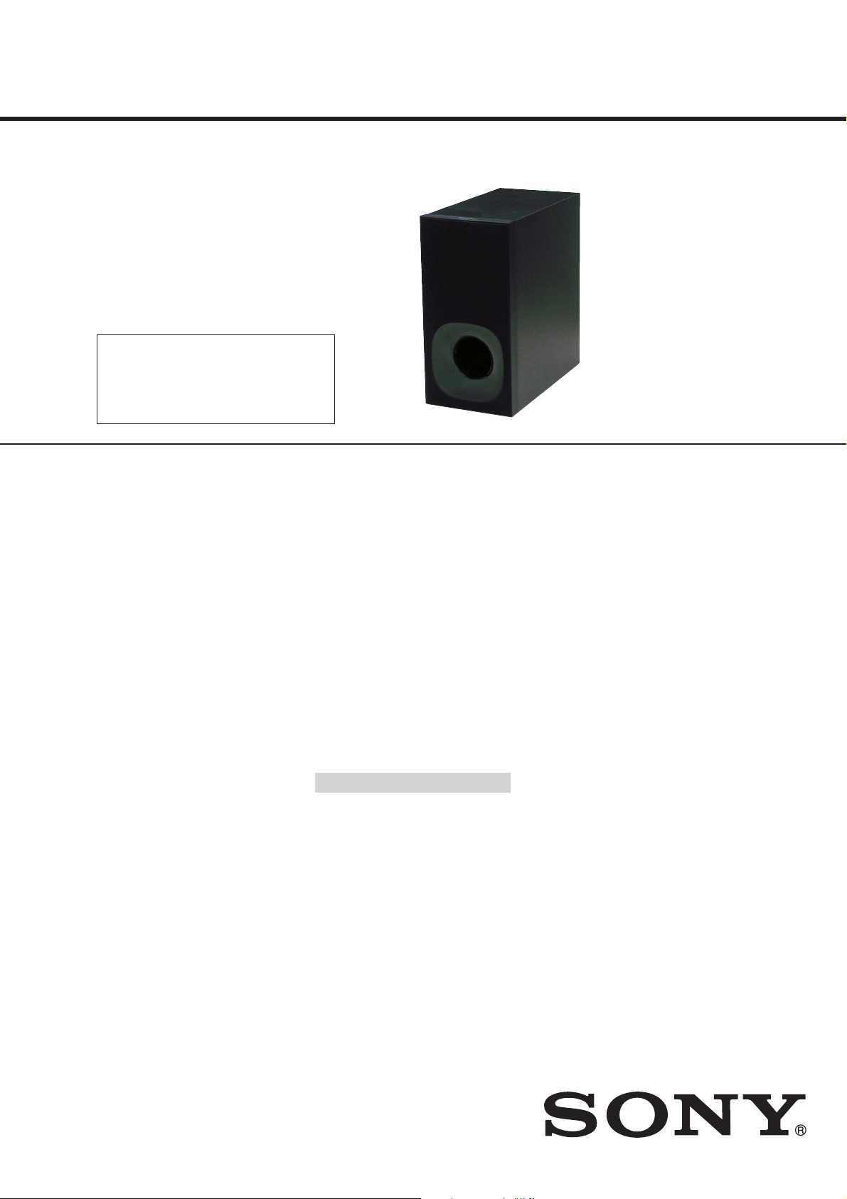
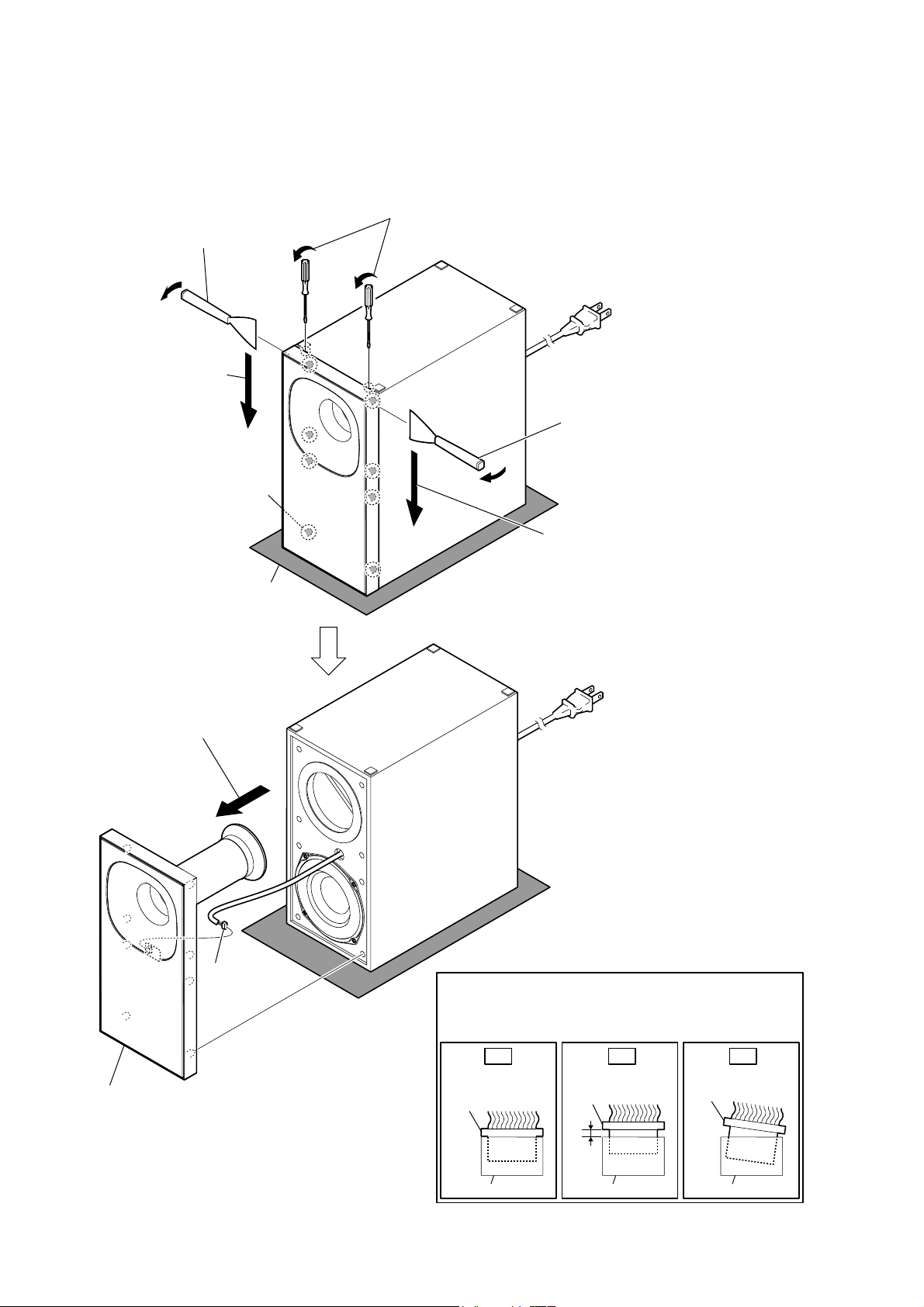
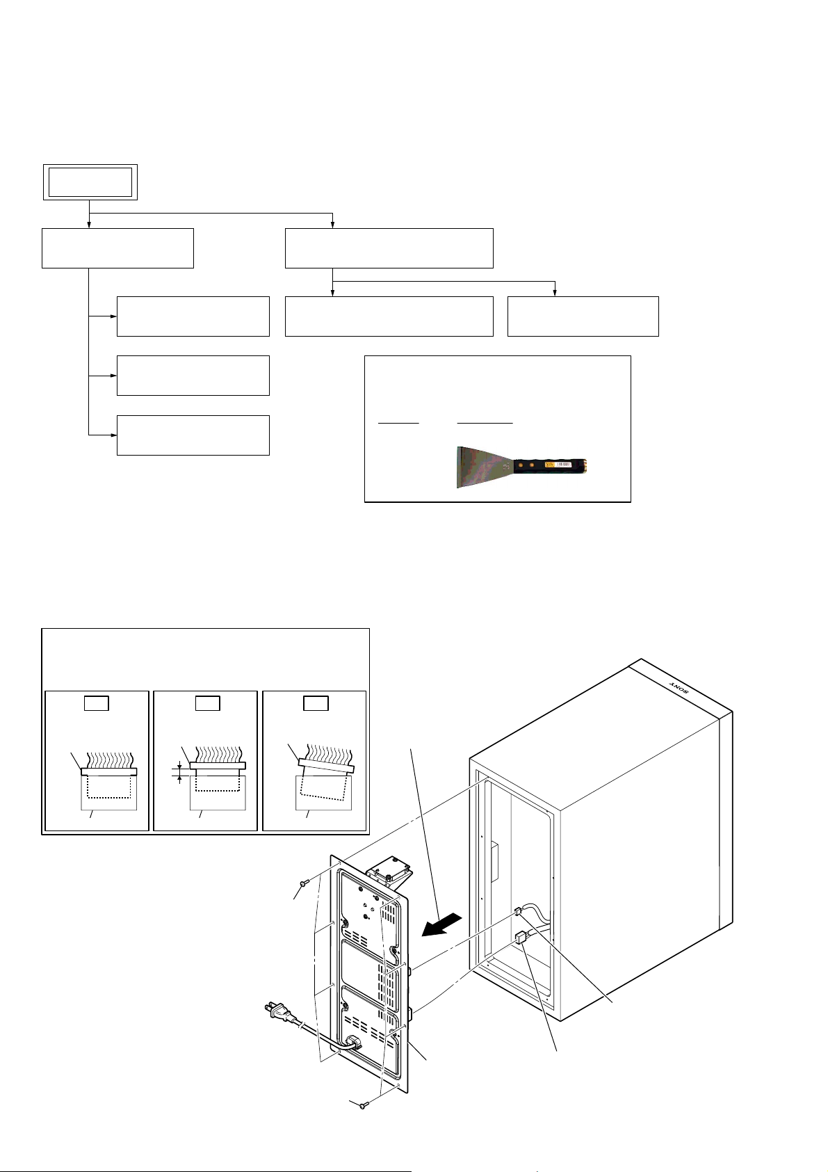
Sony SA-WCT180 User manual

SERVICE MANUAL
Sony Corporation
Published by Sony Techno Create Corporation
SA-WCT180
ACTIVE SUBWOOFER
9-896-126-02
2015E33-1
© 2015.05
US Model
Canadian Model
AEP Model
UK Model
E Model
Australian Model
Chinese Model
Ver. 1.1 2015.05
• SA-WCT180 is the active subwoofer in HT-CT180.
• All of the units included in the HT-CT180 (SA-WCT180/
SA-CT180/Remote control) are required to confirming op-
eration of SA-WCT180. Check in advance that you have
all of the units.
• For the TEST MODE for this unit, refer to the service manual of HT-CT180.
SPECIFICATIONS
POWER OUTPUT (reference)
5
45 W (per channel at 4 ohms, 100 Hz) (Chinese model)
0 W (per channel at 4 ohms, 100 Hz) (Except Chinese model)
Speaker system
Subwoofer system, Bass reflex
Speaker
130 mm (5 1
/8in) cone type
Power requirements
120 V AC, 60 Hz (US and Canadian models)
Power consumption
On: 13 W
Standby mode: 0.5 W or less
Dimensions (approx.) (w/h/d)
170 mm × 342 mm × 325 mm
(6 3/4in × 13 1
/2in × 12 7/8in)
Mass (approx.)
5.5kg(12Ib2oz)
Frequency band
2.4 GHz band (2.404 GHz - 2.476 GHz)
Modulation method
GFSK
Design and specifications are subject to
change without notice.
Wireless receiver
220 V - 240 V AC, 50 Hz/60 Hz (AEP, UK, Indian, Singapore,
Argentina, Thai, Australian and Chinese models)
110 V - 240 V AC, 50 Hz/60 Hz (Latin American model
(Except Argentina))
Note:
Be sure to keep your PC used for service and
checking of this unit always updated with the
latest version of your anti-virus software.
In case a virus affected unit was found during
service, contact your Service Headquarters.

SA-WCT180
2
SAFETY CHECK-OUT
After correcting the original service problem, perform the follow-
ing safety check before releasing the set to the customer:
Check the antenna terminals, metal trim, “metallized” knobs,
screws, and all other exposed metal parts for AC leakage.
Check leakage as described below.
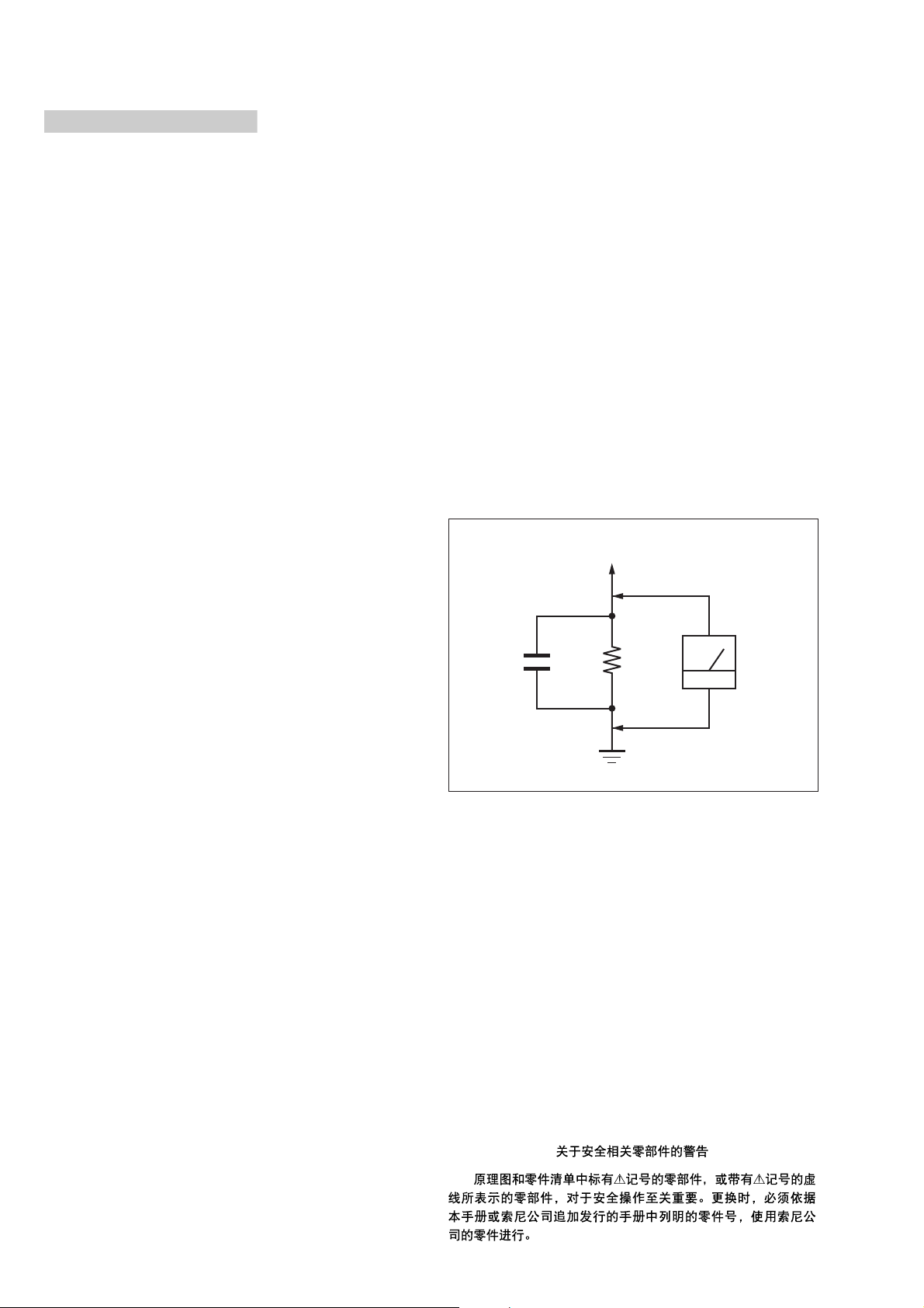
LEAKAGE TEST
The AC leakage from any exposed metal part to earth ground and
from all exposed metal parts to any exposed metal part having a
return to chassis, must not exceed 0.5 mA (500 microamperes.).
Leakage current can be measured by any one of three methods.
1. A commercial leakage tester, such as the Simpson 229 or RCA
WT-540A. Follow the manufacturers’ instructions to use these
instruments.
2. A battery-operated AC milliammeter. The Data Precision 245
digital multimeter is suitable for this job.
3. Measuring the voltage drop across a resistor by means of a
VOM or battery-operated AC voltmeter. The “limit” indication
is 0.75 V, so analog meters must have an accurate low-voltage
scale. The Simpson 250 and Sanwa SH-63Trd are examples
of a passive VOM that is suitable. Nearly all battery operated
digital multimeters that have a 2 V AC range are suitable. (See
Fig. A)
1.5 kΩ0.15 μF
AC
voltmeter
(0.75 V)
To Exposed Metal
Parts on Set
Earth Ground
Fig. A. Using an AC voltmeter to check AC leakage.
The BLUETOOTH®word mark and logos
are registered trademarks owned by
Bluetooth SIG, Inc. and any use of such
marks by Sony Corporation is under
license.
The N Mark is a trademark or registered
trademark of NFC Forum, Inc. in the
United States and in other countries.
Android™ is a trademark of Google Inc.
“ClearAudio+” is a trademark of Sony
Corporation.
Other trademarks and trade names are
those of their respective owners.
This system incorporates Dolby* Digital
Surround System.
* Manufactured under license from
Dolby Laboratories.
Dolby, and the double-D symbol are
trademarks of Dolby Laboratories.
Copyrights and Trademarks
SAFETY-RELATED COMPONENT WARNING!
COMPONENTS IDENTIFIED BY MARK 0OR DOTTED LINE
WITH MARK 0ON THE SCHEMATIC DIAGRAMS AND IN
THE PARTS LIST ARE CRITICAL TO SAFE OPERATION.
REPLACE THESE COMPONENTS WITH SONY PARTS
WHOSE PART NUMBERS APPEAR AS SHOWN IN THIS
MANUAL OR IN SUPPLEMENTS PUBLISHED BY SONY.
ATTENTION AU COMPOSANT AYANT RAPPORT
À LA SÉCURITÉ!
LES COMPOSANTS IDENTIFIÉS PAR UNE MARQUE 0SUR
LES DIAGRAMMES SCHÉMATIQUES ET LA LISTE DES
PIÈCES SONT CRITIQUES POUR LA SÉCURITÉ DE FONC-
TIONNEMENT. NE REMPLACER CES COMPOSANTS QUE
PAR DES PIÈCES SONY DONT LES NUMÉROS SONT DON-
NÉS DANS CE MANUEL OU DANS LES SUPPLÉMENTS
PUBLIÉS PAR SONY.
Ver. 1.1

SA-WCT180
3
SECTION 1
SERVICING NOTES
UNLEADED SOLDER
Boards requiring use of unleaded solder are printed with the lead-
free mark (LF) indicating the solder contains no lead.
(Caution: Some printed circuit boards may not come printed with
the lead free mark due to their particular size)
: LEAD FREE MARK
Unleaded solder has the following characteristics.
• Unleaded solder melts at a temperature about 40 °C higher
than ordinary solder.
Ordinary soldering irons can be used but the iron tip has to be
applied to the solder joint for a slightly longer time.
Soldering irons using a temperature regulator should be set to
about 350 °C.
Caution: The printed pattern (copper foil) may peel away if
the heated tip is applied for too long, so be careful!
• Strong viscosity
Unleaded solder is more viscous (sticky, less prone to flow)
than ordinary solder so use caution not to let solder bridges
occur such as on IC pins, etc.
• Usable with ordinary solder
It is best to use only unleaded solder but unleaded solder may
also be added to ordinary solder.
ADVANCE PREPARATION WHEN CONFIRMING OP-
ERATION
All of the units included in the HT-CT180 (SA-WCT180/SA-
CT180/Remote control) are required to confirming operation of
SA-WCT180. Check in advance that you have all of the units.
DESTINATION ABBREVIATIONS
The following abbreviations for model destinations are used in this
service manual.
• Abbreviations
AR : Argentina model
AUS : Australian model
CH : Chinese model
CND : Canadian model
E12 : Indian model
LA : Latin American model (Except Argentina)
SP : Singapore model
TH : Thai model
1. SERVICING NOTES ............................................. 3
2. DISASSEMBLY
2-1. Disassembly Flow........................................................... 6
2-2. AMP Block ..................................................................... 6
2-3. MAIN Board ................................................................... 7
2-4. POWER Board................................................................ 8
2-5. AC Cord (AC1)............................................................... 9
2-6. Front Panel Block ........................................................... 10
2-7. Loudspeaker (13 cm) (SP1) ............................................ 11
2-8. Grille (SW) Assy............................................................. 11
3. DIAGRAMS
3-1. Block Diagram ................................................................ 12
3-2. Schematic Diagram - MAIN Board (1/3) -..................... 14
3-3. Schematic Diagram - MAIN Board (2/3) -..................... 15
3-4. Schematic Diagram - MAIN Board (3/3) -..................... 16
3-5. Printed Wiring Board - MAIN Board - ........................... 17
3-6. Printed Wiring Board - KEY Board -.............................. 17
3-7. Schematic Diagram - KEY Board - ................................ 17
3-8. Printed Wiring Board - LED Board -.............................. 18
3-9. Schematic Diagram - LED Board -................................. 18
3-10. Printed Wiring Board - POWER Board -........................ 18
3-11. Schematic Diagram - POWER Board - .......................... 19
4. EXPLODED VIEWS
4-1. AMP Section ................................................................... 21
4-2. Front Section................................................................... 22
TABLE OF CONTENTS The SERVICING NOTES contains important information for
servicing. Be sure to read this section before repairing the
unit.
Ver. 1.1

SA-WCT180
4
MODEL IDENTIFICATION
Distinguish by Part No. on the rear plate of a main unit.
Note: The printed contents of following figure model number label may be different from the model number label of a main unit.
– Rear view –
MODEL NUMBER LABEL
Chinese model (CN4)
Thai model (TH1)
US and Canadian models (UC2)
UK model (CEK)
AEP model (CEL)
Australian model (AU1)
4-562-813-0[]
4-562-812-0[]
4-562-809-0[]
4-562-817-0[] 4-575-767-0[]
4-569-254-0[]
4-562-811-0[]
4-562-816-0[]
4-562-822-0[]
4-562-819-0[]
Argentina model (AR2) Singapore model (SP1)
Indian model (E12)
Latin American model (LA9)
(Except Argentina)
Ver. 1.1

SA-WCT180
5
ABOUT PARTS REPAIR OF EACH BOARDS
When each boards installed in this unit are defective, individual
electrical parts that the mount is done cannot be replaced. When
each boards are defective, replace the mounted board or the whole
parts including an applicable board.
Printed wiring board and schematic diagram that have been de-
scribed on this service manual are for reference.
(Printed wiring board and schematic diagram of WIERLESS board
have not described)
WHAT TO DO IF PROTECT
If the on/standby LED blinks red, it is state in the protect. This
state shows an abnormality of the AMP circuit.
In this case, there is a possibility that the MAIN board is defective.
Please replace the MAIN board.
NOTE OF REPLACING THE WIRELESS BOARD
When replaced the WIRELESS board, link of SA-CT180 and SA-
WCT180 will be disconnected.
Before you return repaired unit to customers, please link the SA-
CT180 and SA-WCT180 by the following procedure.
If, in a state in which only one of SA-CT180 or SA-WCT180 is
brought into service field, and replaced the WIRELESS board of
SA-CT180 or SA-WCT180, when returning the repaired unit, be
sure to inform the customers that it is necessary to link the follow-
ing procedure.
Enabling the Secure Link
function
You can specify the wireless connection
to link the Bar Speaker to the subwoofer
using the Secure Link function. This
function can help prevent interference if
you use multiple wireless products or
your neighbors use wireless products.
1Press LINK on the rear of the
subwoofer.
You will hear beeps from the
subwoofer.
2Hold down PAIRING on the Bar
Speaker for 5 seconds, then VOL –
for 5 seconds.
The OPTICAL and ANALOG
indicators ash alternately.
When the Bar Speaker is linked to
the subwoofer, the indicators stop
ashing.
If it failed, the indicators light up for
5 seconds. Try again the above
operation.

SA-WCT180
6
SECTION 2
DISASSEMBLY
• This set can be disassembled in the order shown below.
2-1. DISASSEMBLY FLOW
Note: Follow the disassembly procedure in the numerical order given.
2-2. AMP BLOCK
SET
2-2. AMP BLOCK
(Page 6)
2-3. MAIN BOARD
(Page 7)
2-4. POWER BOARD
(Page 8)
2-5. AC CORD (AC1)
(Page 9)
2-8. GRILLE (SW) ASSY
(Page 11)
2-7. LOUDSPEAKER (13 cm) (SP1)
(Page 11)
2-6. FRONT PANEL BLOCK
(Page 10)
JIG
When disassembling the unit, use the following
jig for speaker removal.
Part No. Description
J-2501-238-A JIG FOR SPEAKER REMOVAL
– Rear view –
1four screws
(3.5 u14 B)
2Remove the AMP block
in the direction of the
arrow.
4LED board cable
connector (XS5)
3 speaker cable connector
(XP8)
5 AMP block
1four screws
(3.5 u14 B)
Insert only part way.Insert straight into
the interior.
connector
Insert at a slant.
connector connector connector
connector connector
OK NG NG
How to install the connector
Insert the connector straight into the interior.
There is a possibility that using this unit without
the connector correctly installed will damage it.

SA-WCT180
7
2-3. MAIN BOARD
– AMP block front view –
:ire VettinJ
3 connector
(CN502)
4two screws
(3 u6 B)
2 connector
(XS6)
1 connector
(XP3)
4two screws
(3 u6 B)
Insert only part way.
Insert straight into
the interior.
connector
Insert at a slant.
connector
connector connector
connector connector
OK
NG NG
+ow to inVtDll tKe connector
Insert the connector straight into the interior.
There is a possibility that using this unit
without the connector correctly installed will
damage it. 5 MAIN board

SA-WCT180
8
2-4. POWER BOARD
– AMP block front view –
:LUHVHWWLQJ
2 connector
(CN501)
3two screws
(3 u6 B)
3two screws
(3 u6 B)
4 POWER board
1 connector
(CN502)
Insert only part way.
Insert straight into
the interior.
connector
Insert at a slant.
connector
connector connector
connector connector
OK
NG NG
+RZWRLQVWDOOWKHFRQQHFWRU
Insert the connector straight into the interior.
There is a possibility that using this unit
without the connector correctly installed will
damage it.

SA-WCT180
9
2-5. AC CORD (AC1)
Note 2: Check the directions of the claw of the cord bush,
and install correctly.
+RZWRLQVWDOOWKHFRUGEXVK
claw
AC cord (AC1)
[white line]
cord bush
125 ± 5 mm
–5HDUYLHZ–
2two claws
5cord bush
3Draw the AC cord block out
of the hole in AMP block.
6AC cord (AC1)
4claw
1connector
(CN501)
–$03EORFNIURQWYLHZ–
cord bush
hole
,QVWDOODWLRQGLUHFWLRQIRUWKH$&FRUGEORFN
claw
cord bush
Note 1: When installing the cord bush to the AC cord (AC1), check the directions of the white line
of the AC cord (AC1) and the claw of the cord bush, and install correctly.
Note 3: Make sure that the white line
is at the bottom.

SA-WCT180
10
2-6. FRONT PANEL BLOCK
Insert only part way.Insert straight into
the interior.
connector
Insert at a slant.
connector connector connector
connector connector
OK NG NG
How to install the connector
Insert the connector straight into the interior.
There is a possibility that using this unit without the connector
correctly installed will damage it.
total eight bosses
1Insert a flat-head screwdriver in
two slits of bottom of the unit, and
lift the front panel block a little.
6 front panel block
Note 3: When installing the front panel block,
remove the used bond and use a new
bond to fix the front panel block.
Note 1: Please spread a sheet under
a unit not to injure cabinet.
4Remove the front panel block
in the direction of the arrow.
5LED board
connector
(XS6)
– Bottom view –
3 While moving the jig in the
direction of the arrow,
remove all bosses and the
front panel block.
2Insert the jig into the space and slowly
remove the front panel block.
Note 2: When using a jig, please work
carefully so as not to damage
the front panel block and speaker
cabinet.
2Insert the jig into the space and slowly
remove the front panel block.
Note 2: When using a jig, please work
carefully so as not to damage
the front panel block and speaker
cabinet.
3 While moving the jig in the
direction of the arrow,
remove all bosses and the
front panel block.

SA-WCT180
SA-WCT180
1111
2-7. LOUDSPEAKER (13 cm) (SP1)
– Front bottom view –
2Lift up the loudspeaker
(13 cm) (SP1) in the
direction of the arrow.
4loudspeaker (13 cm)
(SP1)
3 terminal (wide side)
[red]
3 terminal (narrow side)
[black]
– Front view –
Note: When installing the loudspeaker (13 cm) (SP1),
make sure that there is a position of the speaker
terminal to the position shown in the figure
below.
terminals
position
speaker cord speaker terminal
OK
How to install the speaker terminal
Insert the speaker terminal straight into the interior.
There is a possibility that using this unit without the
speaker terminal correctly installed will damage it.
Insert straight into the interior.
speaker cord speaker terminal
NG
nsert only part way.
1four screws
(3.5 u14 B)
+RZWRLQVWDOOWKHORXGVSHDNHUFP63
2-8. GRILLE (SW) ASSY
– Front panel block rear view –
3grille (SW) assy
1three screws
(3 u8 B)
total twelve bosses
1three screws
(3 u8 B)
2Insert the screwdriver into the screw hole,
and push the grille in the direction of the
arrow to remove the boss.
screwdriver
screw hole

SA-WCT180
SA-WCT180
1212
SECTION 3
DIAGRAMS
3-1. BLOCK DIAGRAM
Pair
KEY *1
Power
KEY *1
Audio
DATA0
MCLKǃBCLKǃLRCLK
IA2S4M
Power Derating(NA) Power
Derating
Circuit(NA)
IIC
Audio
Processor
STA369BWS
Wireless Module FL 50W(4R) 30%
PBTL
Power/Pair
LED *2 Mute
AMP_FAULT
LDO
TJ4203 For STA369BWS ǃLED*2
3.3V
power
signal
POWER
DC-DC
EUP3482A 5V
Wi
r
eless
18V
POWER
SUPPLY
)RU67$%:6
Module
IA2S4M
18V

SA-WCT180
SA-WCT180
1313
For Schematic Diagrams.
Note:
• All capacitors are in μF unless otherwise noted. (p: pF) 50
WV or less are not indicated except for electrolytics and
tantalums.
• All resistors are in Ωand 1/4 W or less unless otherwise
specified.
THIS NOTE IS COMMON FOR PRINTED WIRING BOARDS AND SCHEMATIC DIAGRAMS.
(In addition to this, the necessary note is printed in each block.)
For Printed Wiring Boards.
Note:
• : Pattern from the side which enables seeing.
(The other layers’ patterns are not indicated.)
MAIN board
WIRELESS board
KEY board
POWER board
LED board
Caution:
Pattern face side:
(Conductor Side)
Parts face side:
(Component Side)
Parts on the pattern face side seen
from the pattern face are indicated.
Parts on the parts face side seen from
the parts face are indicated.
Note:
The components identi-
fied by mark 0or dotted
line with mark 0are criti-
cal for safety.
Replace only with part
number specified.
Note:
Les composants identifiés
par une marque 0sont
critiques pour la sécurité.
Ne les remplacer que par
une pièce portant le nu-
méro spécifié.
• Circuit Boards Location

SA-WCT180
SA-WCT180
1414
3-2. SCHEMATIC DIAGRAM - MAIN Board (1/3) -
A
362
D
5
B
C
714
(1/3)MAIN BOARD
1.5V
2.NC
3.NC
4.GND
5.GPIO 33
6.GPIO 26
7.GPIO 17
8.I2C_DAT
9.GND
10.I2C_CLK
11.I2S_DATI
12.I2S_LRCK
13.I2S_BCK
14.GPIO 31
15.I2S_MCLK
16.GND
17.GPIO 1
18.GPIO 2
19.GPIO 3
20.I2C_Busy
STB_5V
STB_3V3
STB_3V3
STB_3V3
1
2
3
4
5
6
7
8
9
10
11
12
13
14
15
16
17
18
19
20
1
2
3
1
2
3
R104 33R104 33
C230 15PFC230 15PF
C100
0.1UF
C100
0.1UF
XP3
20pin/2.0mm
XP3
20pin/2.0mm
R90 1KR90 1K
R87 33R87 33
C228 100pF/50V/NP0
C228 100pF/50V/NP0
C238 100pF/50V/NP0C238 100pF/50V/NP0
R99 560R99 560
C231 10PF/50V/NPO
C231 10PF/50V/NPO
C75 0.1uF/25V/Y5VC75 0.1uF/25V/Y5V
R94 1KR94 1K
C239 100pF/50V/NP0C239 100pF/50V/NP0
C232 10PF/50V/NPOC232 10PF/50V/NPO
C240 100pF/50V/NP0C240 100pF/50V/NP0
C233 10PF/50V/NPOC233 10PF/50V/NPO
R91 33R91 33
C32
22uF/10V/Y5V
C32
22uF/10V/Y5V
R100 68R100 68
R106 33R106 33
R110 33R110 33
FB8 500/200mAFB8 500/200mA
R2210K R2210K
C229 100pF/50V/NP0
C229 100pF/50V/NP0
R86 33R86 33
R103 560R103 560
R2310K R2310K
R107 33R107 33
R111 33R111 33
XS5
3PIN/2.0mm
XS5
3PIN/2.0mm
C97 NC/15PFC97 NC/15PF
C241 100pF/50V/NP0C241 100pF/50V/NP0
R105 33R105 33
R108 33R108 33
R96 33R96 33
Q10 NPN_3DG3904M
Q10 NPN_3DG3904M
XS6
3PIN/2.0mm
XS6
3PIN/2.0mm
R24 NC/10KR24 NC/10K
R93 33R93 33
Q11 NPN_3DG3904M
Q11 NPN_3DG3904M
C98 NC/15PFC98 NC/15PF
R109 33R109 33
C244 100pF/50V/NP0C244 100pF/50V/NP0
R25 NC/10K
R25 NC/10K
R95 33R95 33
C243 100pF/50V/NP0C243 100pF/50V/NP0
C95 NC/15PFC95 NC/15PF
C242 100pF/50V/NP0
C242 100pF/50V/NP0
C245 100pF/50V/NP0C245 100pF/50V/NP0
R92 33R92 33
R97 33R97 33
R98 100R98 100
C99
0.1UF
C99
0.1UF
C96 NC/15PFC96 NC/15PF
1
2
3
4
5
6
7
8
9
10
11
12
13
14
15
16
17
18
19
20
1
2
3
1
2
3
POWER_LED
LINK_LED
POWER_LED
POWER_LED_CON
LINK_LED
LINK_LED_CON
LINK KEY
POWER_KEY
D
D
RESET_AMP
AMP_SDA
AMP_SCL
SUB_DATA
SUB_LRCK
SUB_BCK
1/2power-control
SUB_MCLK
AMP_FAULT
AMP_MUTE1
POWER_LED_CON
LINK_LED_CON
POWER_KEY
LINK KEY

SA-WCT180
SA-WCT180
1515
3-3. SCHEMATIC DIAGRAM - MAIN Board (2/3) - • See page 20 for IC Block Diagrams.
A
386
E
2
D
5
B
C
714
(2/3)MAIN BOARD
Close to U2_EUP3482A
Power-derating OP
POWER_18V
STB_5V
POWER_18V PVDD
STB_5V
STB_3V3
STB_3V3 SYS_3V3
POWER_18V
STB_5V
SYS_5V
1
2
3
4
5
6
1
2
3
5
6
4
8
7
1
43
5
2
C7
100nF
C7
100nF
R4
51K/1%
R4
51K/1%
XS1
6PIN/2.5mm/40mm
XS1
6PIN/2.5mm/40mm
R183
10K
R183
10K
R218 0R218 0
C17
NC/100nF
C17
NC/100nF
L4 10uH/1AL4 10uH/1A
C184
2.2uF
C184
2.2uF
C296
NC/100pF/50V/NP0
C296
NC/100pF/50V/NP0
C183
2.2uF
C183
2.2uF
C84
NC/100nF
C84
NC/100nF
Q20
NC/NPN_3DG3904M
Q20
NC/NPN_3DG3904M
R190
15K
R190
15K
100UF/25V
CE20
100UF/25V
CE20
C36
100nF
C36
100nF
Q547 NC/PNP_MMBT8550CQ547 NC/PNP_MMBT8550C
C3
0.1uF
C3
0.1uF
R26 NC/0R26 NC/0
R170
47K/1%
R170
47K/1%
C18
NC/100nF
C18
NC/100nF
R1
56
R1
56
C4
330pF
C4
330pF
C1
NC/100nF
C1
NC/100nF
R193
NC/10K
R193
NC/10K
C152
NC/330pF
C152
NC/330pF
R5 47KR5 47K
C77
100nF
C77
100nF
R6
22K
R6
22K
R11
7.5K
R11
7.5K
R102
NC/56
R102
NC/56
R13 NC/4.7KR13 NC/4.7K
C76
100nF
C76
100nF
R192 NC/30KR192 NC/30K
D542
NC
D542
NC
U2
EUP3482ADIR1
U2
EUP3482ADIR1
C13
100nF
C13
100nF
U8
TJ4203GSF5-ADJ
U8
TJ4203GSF5-ADJ
C6
10NF
C6
10NF
R194
NC/10K
R194
NC/10K
R12
11K
R12
11K
100uF/16V
CE3
100uF/16V
CE3
C2011uF/50V/X7R C2011uF/50V/X7R
C83 10uF/10V/X7RC83 10uF/10V/X7R
C33
NC/2.2uF
C33
NC/2.2uF
FB19 300/2AFB19 300/2A
C14
3300pF//50V/X7R
C14
3300pF//50V/X7R
++
++
1
2
3
4
5
6
BS
IN
SW
FB
COMP
GND
SS
EN
VIN
ADJ/SENSEEN
VOUT
GND
300mA 2.5V-6V
0.8*(47+15)/15=3.3v
45mA
D
D
D
DD
DDD
D
D
LINK_LED_CON

SA-WCT180
SA-WCT180
1616
3-4. SCHEMATIC DIAGRAM - MAIN Board (3/3) -
A
386
E
2 9
D
5
B
C
714
(3/3)MAIN BOARD
4.7K => 2.7K
10 => 33
4V => 3.5V
SUB+
SUB-
+3.3VD1
+3.3VD2
+3.3VD2
+3.3VD1
SYS_3V3
PVDD
+3.3VD1 +3.3VD2
SYS_5V
+3.3VD1
+3.3VD2
AMP_18V
+3.3VD1
+3.3VD1
+3.3VD1
+3.3VD1
1
2
1
2
3
4
5
6
7
8
9
10
11
12
13
14
15
16
17
1819
20
21
22
23
24
25
26
27
28
29
30
31
32
33
34
35
36
37
3
2
1
84
Power Derating Circuit
C70
1000pF/50V/X7R C70
1000pF/50V/X7R
R47
4.7K
R47
4.7K
R179 NC/1.8KR179 NC/1.8K
Q756
PNP_3CG3906M
Q756
PNP_3CG3906M
C43
330pF
C43
330pF
C391uF C391uF
FB17 70/3AFB17 70/3A
C71
1000pF/50V/X7R C71
1000pF/50V/X7R
C380.1uF C380.1uF
R180
NC/2.4K
R180
NC/2.4K
C41
1000pF/50V/X7R
C41
1000pF/50V/X7R
C530
10uF/16V/X7R
C530
10uF/16V/X7R
R178 NC/560R178 NC/560
R187
NC/2.7K
R187
NC/2.7K
C561000pF/50V/X7R C561000pF/50V/X7R
C53 680pFC53 680pF
C510.22ȝFC510.22ȝF
C64 10PF/50V/NPOC64 10PF/50V/NPO
R182
NC/7.5K
R182
NC/7.5K
C74 10PF/50V/NPOC74 10PF/50V/NPO
C40
0.1uF
C40
0.1uF
CE8
100uF/16V
CE8
100uF/16V
C52 0.1uFC52 0.1uF
R64NC/0 R64NC/0
C62
33pF/50V/NP0
C62
33pF/50V/NP0
C65
0.1uF
C65
0.1uF
FB32 500/200mAFB32 500/200mA
R188
NC/8.2K
R188
NC/8.2K
C47
0.01uF/50V/X7R
C47
0.01uF/50V/X7R
R185
33
R185
33
C57 0.1uF
C57 0.1uF
R85 4.7K
R85 4.7K
C42
0.1uF
C42
0.1uF
D4
NC/LL4148
D4
NC/LL4148
R60 10KR60 10K
C60
330pF
C60
330pF
R5810K R5810K
R68
0
R68
0
R775 220KR775 220K
C49 0.1uFC49 0.1uF
C54
4700pF
C54
4700pF
C769
0.22UF/50V/Y5V
C769
0.22UF/50V/Y5V
C44 0.1uFC44 0.1uF
C63 10PF/50V/NPOC63 10PF/50V/NPO
C37
0.1uF
C37
0.1uF
L2 10uH/5AL2 10uH/5A
C160 NC/1uF/50V/X7RC160 NC/1uF/50V/X7R
R49 33R49 33
XP8
2PIN/7.92mm
XP8
2PIN/7.92mm
C661000pF/50V/X7R C661000pF/50V/X7R
R487
10K
R487
10K
R55
22/5%
R55
22/5%
C16
NC/2.2uF
C16
NC/2.2uF
R65NC/0 R65NC/0
R184
NC/4.7K
R184
NC/4.7K
FB16 70/3AFB16 70/3A
R486
4.7K
R486
4.7K
U6
STA369BWS
U6
R59
2.2K
R59
2.2K
R488
10K
R488
10K
NC/100uF/16V
CE19
NC/100uF/16V
CE19
Q24
NPN_3DG3904M
Q24
NPN_3DG3904M
R63 0R63 0
R782
100
R782
100
NC/47uF/25VCE17 NC/47uF/25VCE17
C159 1uF/50V/X7RC159 1uF/50V/X7R
R186
NC/1.2K/1%
R186
NC/1.2K/1%
R84 4.7K
R84 4.7K
C500.22ȝFC500.22ȝF
L3 10uH/5AL3 10uH/5A
R88 4.7K
R88 4.7K
C86
NC/100nF
C86
NC/100nF
C85
NC/100nF
C85
NC/100nF
C61
33pF/50V/NP0
C61
33pF/50V/NP0
R783
100K
R783
100K
R62
22/5%
R62
22/5%
C68
47pF/50V/NP0
C68
47pF/50V/NP0
U15A
NC/F4558
U15A
NC/F4558
R776
220K
R776
220K
R67NC/0 R67NC/0
C55 0.1uFC55 0.1uF
C226
1000pF/50V/NP0
C226
1000pF/50V/NP0
C45
0.1uF
C45
0.1uF
C227 1000pF/50V/NP0C227 1000pF/50V/NP0
Q5
NPN_3DG3904M
Q5
NPN_3DG3904M
FB33 500/200mAFB33 500/200mA
C580.1uF C580.1uF
Q757
PNP_3CG3906M
Q757
PNP_3CG3906M
C88
100nF
C88
100nF
R66NC/0 R66NC/0
R48 33R48 33
CE9
470uF/35V CE9
470uF/35V
C207
0.1uF
C207
0.1uF
R69 4.7K
R69 4.7K
R52 6.2
R52 6.2
R54 6.2
R54 6.2
R53 33R53 33
C48 10PF/50V/NPOC48 10PF/50V/NPO
C591uF C591uF
R781 220KR781 220K
++
++
++
+
-
+
-
++
1
2
GND_SUB
SA
TEST_MODE
VSS
VCC_REG
OUT2B
GND2
VCC2
OUT2A
OUT1B
VCC1
GND1
OUT1A
GND_REG
VDD
CONFIG
OUT3B / FFX3B
OUT3A / FFX3AEAPD / OUT4B
TWARN / OUT4A
VDD_DIG
GND_DIG
PWRDN
VDD_PLL
FILTER_PLL
GND_PLL
XTI
BICKI
LRCKI
SDI
RESET
INT_LINE
SDA
SCL
GND_DIG
VDD_DIG
GND
6mA
SUB+
SUB-
AMP_18V
AMP_MUTE
SUB+
AMP_RST
AMP_SCL
AMP_SDA
D
SUB_MCLK
SUB_BCK
SUB_LRCK
SUB_DATA
AMP_SCL
AMP_SDA
1/2power-control
AMP_FAULT
AMP_MUTE1
AMP_FAULT
RESET_AMP
• See page 20 for IC Pin Function Description.

SA-WCT180
SA-WCT180
1717
3-5. PRINTED WIRING BOARD - MAIN Board -
A
B
C
D
E
1 2 3 4
MAIN BOARD (COMPONENT SIDE) MAIN BOARD (CONDUCTOR SIDE)
• : Uses unleaded solder.
• See page 13 for Circuit Boards Location.
3-6. PRINTED WIRING BOARD - KEY Board -
KEY BOARD (COMPONENT SIDE) KEY BOARD (CONDUCTOR SIDE)
A
B
1 2 3 4
• : Uses unleaded solder.
• See page 13 for Circuit Boards Location.
3-7. SCHEMATIC DIAGRAM - KEY Board -
A
32
B
1
KEY BOARD
ES1:
A:46-FH010T-04IF
B:46-FH006T-04HP
ES2:
46-FH008T-03P
1
2
3
XP5
3PIN/2.0mm
XP5
3PIN/2.0mm
C17
NC/0.1uF
C17
NC/0.1uF
C19
NC/0.1uF
C19
NC/0.1uF
SW1 POWERSW1 POWER
SW2 LINKSW2 LINK
D
D
1
2
3

SA-WCT180
SA-WCT180
1818
3-10. PRINTED WIRING BOARD - POWER Board -
POWER BOARD (COMPONENT SIDE) POWER BOARD (CONDUCTOR SIDE)
A
B
C
D
E
1 2 3 4 5 6
3-8. PRINTED WIRING BOARD - LED Board -
LED BOARD (COMPONENT SIDE) LED BOARD (CONDUCTOR SIDE)
A
1 2 3
• : Uses unleaded solder.
• See page 13 for Circuit Boards Location.
3-9. SCHEMATIC DIAGRAM - LED Board -
PIN-1 GREEN
PIN-3 RED
ES1:
46-FF034T-04H, change to 3PIN
1
2
3
1
2
3
XS6
3PIN/2.0mm
XS6
3PIN/2.0mm
LED1
LED_3P_2PARTA
LED1
LED_3P_2PARTA
C3
NC/0.1uF
C3
NC/0.1uF
C16
NC/0.1uF
C16
NC/0.1uF
LED_LINK
LED_POWER
D
D
1
2
3
A
2
B
1
LED BOARD
• : Uses unleaded solder.
• See page 13 for Circuit Boards Location.

SA-WCT180
SA-WCT180
1919
3-11. SCHEMATIC DIAGRAM - POWER Board - • See page 20 for IC Block Diagrams.
A
36
E
2
D
5
B
C
714
POWER BOARD
1
2
1
2
3
4
14
23
3
5
6
1
2
8
12
9
11
14
23
1
2
3
4
5
6
3
1
2
1
2
3
12
43
4
6
7
1
3
11
8
9
12
2
1
3
4
C534
0.1uF/50V/X7R
C534
0.1uF/50V/X7R
CY503
NC/220pF/250VAC
CY503
NC/220pF/250VAC
R543 100KR543 100K
R570 0R570 0
CN501
2PIN/7.92mm
CN501
2PIN/7.92mm
R502D
1M
R502D
1M
FB503
NC/FB90@100MHz
FB503
NC/FB90@100MHz
FB501
FB90@100MHz
FB501
FB90@100MHz
R536
2M/5%
R536
2M/5%
C549
0.1uF/50V/X7R
C549
0.1uF/50V/X7R
R542
1.5K
R542
1.5K
R531
NC
R531
NC
47uF/35V
CE531
47uF/35V
CE531
CY506 1000pF/250VACCY506 1000pF/250VAC
CN502
4PIN/2.5mm
CN502
4PIN/2.5mm
C535 220pF/50V/X7RC535 220pF/50V/X7R
R541
680
R541
680
R502A
1M
R502A
1M
U531
TOP256EN
U531
TOP256EN
R565
22
R565
22
ZD531
12V
ZD531
12V
LIF501
LIF4-22-15
LIF501
LIF4-22-15
CY507 nc/470pF/250VACCY507 nc/470pF/250VAC
D533
NC/MUR420/4A/200V
D533
NC/MUR420/4A/200V
ZD532
27V
ZD532
27V
R533
0
R533
0
R534
47K/2W
R534
47K/2W
T5311
NC/ER28
T5311
NC/ER28
R510
NC/10
R510
NC/10
R502B
1M
R502B
1M
LIF502
NC/LIF4-22-15
LIF502
NC/LIF4-22-15
TR501
NTC/3ohm/5A
TR501
NTC/3ohm/5A
ZD534
NC/BZX79C24
ZD534
NC/BZX79C24
R540
0
R540
0
R557
20k
R557
20k
CY502
470pF/250VAC
CY502
470pF/250VAC
C536
100pF/1KV
C536
100pF/1KV
R544
75
R544
75
CY501
470pF/250VAC
CY501
470pF/250VAC
NC/MUR420/4A/200VNC/MUR420/4A/200V
C533
2200pF/1KV
C533
2200pF/1KV
CN503
6PIN/2.5mm/120mm
CN503
6PIN/2.5mm/120mm
FB502
FB90@100MHz
FB502
FB90@100MHz
R532
NC
R532
NC
R569 0R569 0
C531
4700pF/1KV
C531
4700pF/1KV
R539
100
R539
100 U533
AS431
U533
AS431
R537
2M/5%
R537
2M/5%
CX501
0.33uF/275VAC
CX501
0.33uF/275VAC
D538
SB20A200
D538
SB20A200
C532
0.1uF/50V/X7R
C532
0.1uF/50V/X7R 47uF/35V
CE532
47uF/35V
CE532
D531
FR207/2A/1000V
D531
FR207/2A/1000V
100uF/450V
CE502
100uF/450V
CE502
D532
FR104/1A/400V
D532
FR104/1A/400V
U532
LTV-817S-B
U532
LTV-817S-B
R538
5.6
R538
5.6
820uF/50V
CE533
820uF/50V
CE533
T5311-1
EF25
T5311-1
EF25
R546
30k
R546
30k
BD1
KBP306
BD1
KBP306
F501
T3.15A 250V
F501
T3.15A 250V
RV501
VDR/560V
RV501
VDR/560V
R502C
1M
R502C
1M
++
C
S
DV
F
CONTROL
X
C
S
DV
F
CONTROL
X
++
++
++
-+ -+
Alternative
1.18V
2.18V
3.18V
4.GND
5.GND
6.GND
PG
HV
VDD
D
FB
HV
+18V
HV
GND
VDD
D
FB
PG
GND
+18V
1
2
1
2
3
4
D
P-GND
FB
VDD
N.C
A8
A10
A9
A10
1
2
3
4
5
6
D
P-GND
FB
VDD
N.C
A12
A9
A12
A13

SA-WCT180
SA-WCT180
2020
• IC Block Diagrams
– MAIN Board –
U2 EUP3482ADIR1
– POWER Board –
U531 TOP256EN
6+87'2:1
$8725(67$57
&/2&.
&21752//('
785121
*$7('5,9(5
&855(17/,0,7
&203$5$725
,17(51$/89
&203$5$725
,17(51$/
6833/<
9
9
6285&(6
6285&(6
6
5
4
'0$;
6723 62)7
67$57
&21752/&
92/7$*(
021,7 259
)5(48(1&<
)
9
,)%
9
=&
9
&
/($',1*
('*(
%/$1.,1*
¹
+<67(5(7,&
7+(50$/
6+87'2:1
6+8175(*8/$725
(5525$03/,),(5
'5$,1'
212))
'& 0$;
'& 0$;
NN
29
89
293 9
9,/,0,7
&855(17
/,0,7
$'-867
9%* 9 7
/,1(
6(16(
62)767$57
2))
)5('8&7,21
)5('8&7,21
6723/2*,&
(;7(51$/
&855(17
/,0,7;
26&,//$725
:,7+-,77(5
3:0
.36833(5
.36/2:(5
62)767$57
,)%
,36833(5
,36/2:(5
.36833(5
.36/2:(5
• IC Pin Function Description
MAIN BOARD U6 STA369BWS (DIGITAL AMP)
Pin No. Pin Name I/O Description
1 GND_SUB - Ground terminal
2 SA I I2C select address signal input terminal Fixed at “H” in this unit
3 TEST_MODE I Fixed at “L” in this unit
4 VSS I/O Internal reference voltage (–3.3V) input/output terminal
5 VCC_REG I/O Internal reference voltage input/output terminal
6 OUT2B O Audio signal (subwoofer) output terminal
7 GND2 - Ground terminal
8 VCC2 - Power supply terminal
9 OUT2A O Audio signal (subwoofer) output terminal
10 OUT1B O Audio signal (subwoofer) output terminal
11 VCC1 - Power supply terminal
12 GND1 - Ground terminal
13 OUT1A O Audio signal (subwoofer) output terminal
14 GND_REG - Internal reference ground terminal
15 VDD I Internal reference voltage (+3.3V) input terminal
16 CONFIG I Parallel mode command signal input terminal Fixed at “H” in this unit
17 OUT3B/FFX3B O Not used
18 OUT3A/FFX3A O Not used
19 EPAD/OUT4B O Not used
20 TWARN/OUT4A I/O Not used
21 VDD_DIG - Power supply terminal (+3.3V)
22 GND_DIG - Ground terminal
23 PWRDN I Muting signal input terminal
24 VDD_PLL - Power supply terminal (+3.3V) (for PLL)
25 FILTER_PLL I Connection to PLL filter terminal
26 GND_PLL - Ground terminal (for PLL)
27 XTI I Master clock signal input terminal
28 BICKI I Bit clock signal input terminal
29 LRCKI I L/R sampling clock signal input terminal
30 SDI I Audio data (subwoofer) input terminal
31 RESET I Reset signal input terminal
32 INT_LINE O Fault signal output terminal
33 SDA I Serial data input terminal
34 SCL I Clock signal input terminal
35 GND_DIG - Ground terminal
36 VDD_DIG - Power supply terminal (+3.3V)
37 GND - Ground terminal
Table of contents
Other Sony Subwoofer manuals

Sony
Sony SA-WM40 User manual

Sony
Sony XS-GTR100L Installation instructions manual

Sony
Sony XS-L102P5S Product guide

Sony
Sony SA-WX700 User manual

Sony
Sony SA-SC8 User manual

Sony
Sony SA-WMSP69 User manual

Sony
Sony XS-L1235 Product guide

Sony
Sony XS-L1535 User manual

Sony
Sony SA-WMS356 User manual

Sony
Sony XS XS-L121P5 User manual