Sony SA-WCT770 User manual

SERVICE MANUAL
Sony Corporation
Published by Sony Techno Create Corporation
SA-WCT770
ACTIVE SUBWOOFER
9-893-983-02
2014F33-1
© 2014.06
US Model
Canadian Model
AEP Model
UK Model
Australian Model
Chinese Model
Saudi Arabia Model
Singapore Model
Taiwan Model
Ver. 1.1 2014.06
• SA-WCT770 is the active subwoofer in HT-CT770.
• All of the units included in the HT-CT770 (SA-WCT770/
SA-CT770) are required to confirming operation of SA-
WCT770. Check in advance that you have all of the units.
• For the TEST MODE for this unit, refer to the service manual of HT-CT770.
SPECIFICATIONS
POWER OUTPUT (reference)
120 W (per channel at 4 ohms, 100 Hz) (Except Chinese model)
75W (per channel at 4 ohms, 100 Hz) (Chinese model)
Speaker system
Subwoofer system, Bass reflex
Speaker
160 mm (6 3/8 in) cone type
Rated impedance
4 ohms
Power requirements
120 V AC, 60 Hz (US and Canadian models)
220 V - 240 V AC, 50 Hz/60 Hz (AEP, UK, Australian, Chinese and Singapore models)
110 V - 240 V AC, 50 Hz/60 Hz (Saudi Arabia model)
120 V AC, 50 Hz/60 Hz (Taiwan model)
Power consumption
On: 30 W
Standby mode: 0.5 W or less
Dimensions (approx.) (w/h/d)
271 mm × 404 mm × 271 mm
(10 3/4 in × 16 in × 10 3/4 in)
Mass (approx.)
8.8 kg (17 Ib 10 1/2 oz)
Speaker system
Wireless Sound Specification version 2.0
Frequency band
2.4 GHz (2.4000 GHz - 2.4835 GHz)
Modulation method
Pi / 4 DQPSK
Wireless receiver section
Design and specifications are subject to change without notice.

SA-WCT770
2
NOTES ON CHIP COMPONENT REPLACEMENT
• Never reuse a disconnected chip component.
• Notice that the minus side of a tantalum capacitor may be dam-
aged by heat.
SAFETY CHECK-OUT
After correcting the original service problem, perform the follow-
ing safety check before releasing the set to the customer:
Check the antenna terminals, metal trim, “metallized” knobs,
screws, and all other exposed metal parts for AC leakage.
Check leakage as described below.
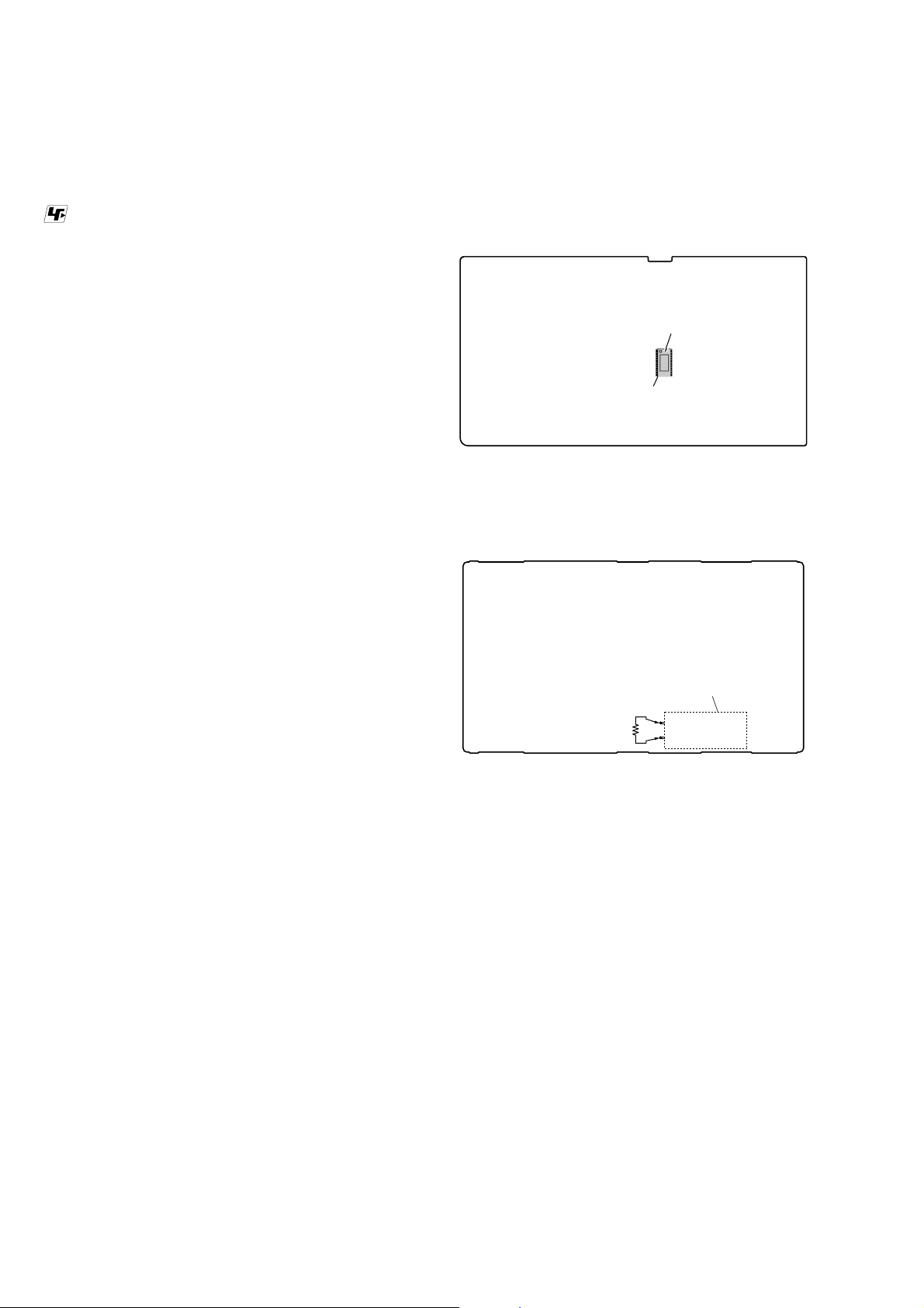
LEAKAGE TEST
The AC leakage from any exposed metal part to earth ground and
from all exposed metal parts to any exposed metal part having a
return to chassis, must not exceed 0.5 mA (500 microamperes.).
Leakage current can be measured by any one of three methods.
1. A commercial leakage tester, such as the Simpson 229 or RCA
WT-540A. Follow the manufacturers’ instructions to use these
instruments.
2. A battery-operated AC milliammeter. The Data Precision 245
digital multimeter is suitable for this job.
3. Measuring the voltage drop across a resistor by means of a
VOM or battery-operated AC voltmeter. The “limit” indication
is 0.75 V, so analog meters must have an accurate low-voltage
scale. The Simpson 250 and Sanwa SH-63Trd are examples
of a passive VOM that is suitable. Nearly all battery operated
digital multimeters that have a 2 V AC range are suitable. (See
Fig. A)
1.5 kΩ0.15 μF
AC
voltmeter
(0.75 V)
To Exposed Metal
Parts on Set
Earth Ground
Fig. A. Using an AC voltmeter to check AC leakage.
T
his system incorporates Dolby* Digital and the DTS** Digital Surround
System.
* Manufactured under license from Dolby Laboratories.
Dolby, and the double-D symbol are trademarks of Dolby
Laboratories.
** Manufactured under license under U.S. Patent Nos: 5,956,674;
5,974,380; 6,226,616; 6,487,535; 7,212,872; 7,333,929; 7,392,195;
7,272,567 & other U.S. and worldwide patents issued & pending.
DTS-HD, the Symbol, & DTS-HD and the Symbol together are
registered trademarks of DTS, Inc.
Product includes software. © DTS, Inc. All Rights Reserved.
The BLUETOOTH® word mark and logos are registered trademarks owned
by Bluetooth SIG, Inc. and any use of such marks by Sony Corporation is
under license.
This system incorporates High-Definition Multimedia Interface (HDMI™)
technology.
T
he terms HDMI and HDMI High-Definition Multimedia Interface, and the
HDMI Logo are trademarks or registered trademarks of HDMI Licensing
LLC in the United States and other countries.
“BRAVIA” logo is a trademark of Sony Corporation.
“DSEE” is a trademark of Sony Corporation.
“x.v.Color” and “x.v.Color” logo are trademarks of Sony Corporation.
“PlayStation®” is a registered trademark of Sony Computer Entertainment
Inc.
T
he N Mark is a trademark or registered trademark of NFC Forum, Inc. in
the United States and in other countries.
Android and Google Play are trademarks of Google Inc.
"ClearAudio+" is a trademark of Sony Corporation.
Apple, the Apple logo, iPhone, iPod, and iPod touch are trademarks of
Apple Inc., registered in the U.S. and other countries. App Store is a
service mark of Apple Inc.
“Made for iPod,” and “Made for iPhone” mean that an electronic
accessory has been designed to connect specifically to iPod or iPhone,
respectively, and has been certified by the developer to meet Apple
performance standards. Apple is not responsible for the operation of this
device or its compliance with safety and regulatory standards. Please
note that the use of this accessory with iPod or iPhone may affect
wireless performance.
Made for iPod/iPhone models
The compatible iPod/iPhone models are as follows. Update your iPod/
iPhone with the latest software before using with the system.
BLUETOOTH technology works with:
iPhone
iPhone 5s/iPhone 5c/iPhone 5/iPhone 4s/iPhone 4/iPhone 3GS
iPod touch
iPod touch (5th generation)/iPod touch (4th generation)
Other trademarks and trade names are those of their respective owners.
Copyrights
SAFETY-RELATED COMPONENT WARNING!
COMPONENTS IDENTIFIED BY MARK 0OR DOTTED LINE
WITH MARK 0ON THE SCHEMATIC DIAGRAMS AND IN
THE PARTS LIST ARE CRITICAL TO SAFE OPERATION.
REPLACE THESE COMPONENTS WITH SONY PARTS
WHOSE PART NUMBERS APPEAR AS SHOWN IN THIS
MANUAL OR IN SUPPLEMENTS PUBLISHED BY SONY.
ATTENTION AU COMPOSANT AYANT RAPPORT
À LA SÉCURITÉ!
LES COMPOSANTS IDENTIFIÉS PAR UNE MARQUE 0SUR
LES DIAGRAMMES SCHÉMATIQUES ET LA LISTE DES
PIÈCES SONT CRITIQUES POUR LA SÉCURITÉ DE FONC-
TIONNEMENT. NE REMPLACER CES COMPOSANTS QUE
PAR DES PIÈCES SONY DONT LES NUMÉROS SONT DON-
NÉS DANS CE MANUEL OU DANS LES SUPPLÉMENTS
PUBLIÉS PAR SONY.
Ver. 1.1

SA-WCT770
3
1. SERVICING NOTES ............................................. 4
2. DISASSEMBLY
2-1. Disassembly Flow........................................................... 6
2-2. Rear Panel Block ............................................................ 6
2-3. Top Panel Block.............................................................. 7
2-4. SUB LED Board ............................................................. 8
2-5. Sub AMP Block .............................................................. 8
2-6. Top Plate Block, Fuse (F900) ......................................... 9
2-7. POWER Board................................................................ 9
2-8. Power Cord (AC1) .......................................................... 10
2-9. RF Modulator (SWA12-4V RX) (RF1) .......................... 11
2-10. Rear Plate Block ............................................................. 11
2-11. SUB MAIN Board .......................................................... 12
2-12. Bottom Panel Block ........................................................ 13
2-13. Loudspeaker (16 cm) (SP1) ............................................ 14
3. TROUBLESHOOTING .......................................... 15
4. DIAGRAMS
4-1. Block Diagram................................................................ 16
4-2. Printed Wiring Board - SUB MAIN Board (Side A) -.... 18
4-3. Printed Wiring Board - SUB MAIN Board (Side B) -.... 19
4-4. Schematic Diagram - SUB MAIN Board (1/2) - ............ 20
4-5. Schematic Diagram - SUB MAIN Board (2/2) - ............ 21
4-6. Printed Wiring Board - POWER Board -........................ 22
4-7. Schematic Diagram - POWER Board - .......................... 23
4-8. Printed Wiring Boards
- SUB LED/SUB KEY Boards -..................................... 24
4-9. Schematic Diagram - SUB LED/SUB KEY Boards - .... 24
5. EXPLODED VIEWS
5-1. Overall Section ............................................................... 29
5-2. Sub AMP Section ............................................................ 30
5-3. Subwoofer Cabinet Section ............................................ 31
6. ELECTRICAL PARTS LIST .............................. 32
TABLE OF CONTENTS

SA-WCT770
4
SECTION 1
SERVICING NOTES
UNLEADED SOLDER
Boards requiring use of unleaded solder are printed with the lead-
free mark (LF) indicating the solder contains no lead.
(Caution: Some printed circuit boards may not come printed with
the lead free mark due to their particular size)
: LEAD FREE MARK
Unleaded solder has the following characteristics.
• Unleaded solder melts at a temperature about 40 °C higher
than ordinary solder.
Ordinary soldering irons can be used but the iron tip has to be
applied to the solder joint for a slightly longer time.
Soldering irons using a temperature regulator should be set to
about 350 °C.
Caution: The printed pattern (copper foil) may peel away if
the heated tip is applied for too long, so be careful!
• Strong viscosity
Unleaded solder is more viscous (sticky, less prone to flow)
than ordinary solder so use caution not to let solder bridges
occur such as on IC pins, etc.
• Usable with ordinary solder
It is best to use only unleaded solder but unleaded solder may
also be added to ordinary solder.
ADVANCE PREPARATION WHEN CONFIRMING OP-
ERATION
All of the units included in the HT-CT770 (SA-WCT770/SA-
CT770) are required to confirming operation of SA-WCT770.
Check in advance that you have all of the units.
NOTE OF PERFORMING THE OPERATION CHECK IN
THE STATE THAT HEAT SINK WAS REMOVED
When performing the operation check in the state that this unit was
disassembled, it is possible to perform the operation check in the
state that heat sink was removed. But don’t perform the operation
check in the long time, and perform the operation check in the
volume state as low as possible.
“PRTECT (PROTECT)” APPEARS ON THE DISPLAY OF
THE BAR SPEAKER (SA-CT770)
qPress the ÒÄÆ (on/standby) button to turn off the system. After the
indicator disappears, disconnect the AC power cord (mains lead)
then check that nothing is blocking the ventilation holes of the
system.
NOTE OF REPLACING THE IC104 ON THE SUB MAIN
BOARD AND THE COMPLETE SUB MAIN BOARD
When IC104 on the SUB MAIN board and the complete SUB
MAIN board are replaced, it is necessary to spread the compound
between the SUB MAIN board and the heat sink.
Spread the compound (THERMAL COMPOUND (G747)) refer-
ring to the figure below.
– SUB MAIN Board (Side A) –
IC104
thermal compound (G747)
CAPACITOR ELECTRICAL DISCHARGE PROCESSING
When checking the board, for the electric shock prevention, con-
nect the resistors to both ends of respective capacitor (C935 or
C936) to discharge the capacitor (C935 or C936).
– POWER Board (Conductor Side) –
800 :/2 W
C935 (US, Canadian and Taiwan models)
C936 (Except US, Canadian and Taiwan models)
Ver. 1.1

SA-WCT770
5
MODEL IDENTIFICATION
Distinguish by model number label printed on the rear plate of a main unit.
Note: The printed contents of following figure model number label may be different from the model number label of a main unit.
– Rear view –
– Rear view –
US and Canadian models
MODEL NUMBER LABEL
4-488-123-0[] UC
MODEL NUMBER LABEL
Part No.
Destination code
Destination Part No. Destination code
AEP, UK 4-488-132-0[] CEL
Singapore 4-529-514-1[] SP1
Australian 4-529-515-1[] AU1
Taiwan 4-529-591-0[] TW2
Chinese 4-529-593-0[] CN4
Saudi Arabia 4-531-646-1[] EA3
Ver. 1.1

SA-WCT770
6
SECTION 2
DISASSEMBLY
• This set can be disassembled in the order shown below.
2-1. DISASSEMBLY FLOW
Note: Follow the disassembly procedure in the numerical order given.
2-2. REAR PANEL BLOCK
SET
2-8. POWER CORD (AC1)
(Page 10)
2-5. SUB AMP BLOCK
(Page 8)
2-2. REAR PANEL BLOCK
(Page 6)
2-3. TOP PANEL BLOCK
(Page 7)
2-7. POWER BOARD
(Page 9)
2-10. REAR PLATE BLOCK
(Page 11)
2-11. SUB MAIN BOARD
(Page 12)
2-9. RF MODULATOR (SWA12-4V RX) (RF1)
(Page 11)
2-13. LOUDSPEAKER (16 cm) (SP1)
(Page 14)
2-12. BOTTOM PANEL BLOCK
(Page 13)
2-4. SUB LED BOARD
(Page 8)
2-6. TOP PLATE BLOCK, FUSE (F900)
(Page 9)
1five screws
(BVTP3 u8)
3Pull out the power cord.
2Remove the rear panel block
in the direction of an arrow.
4rear panel block
– Rear view –
• JIG
When disassembling the set, use the following jig (for speaker
removal).
Part No. Description
J-2501-238-A JIG FOR SPEAKER REMOVAL

SA-WCT770
7
2-3. TOP PANEL BLOCK
total four bosses
5connector
(CN901)
6top panel block
– Rear view –
3 All bosses are removed while moving
jig in the direction of the arrow, and
top panel block is removed.
3 All bosses are removed while moving
jig in the direction of the arrow, and
top panel block is removed.
2 Insert the jig into a space and raise
top panel block.
Note 2: When using a jig, please work so
as not to injure top panel block.
2 Insert the jig into a space and raise
top panel block.
Note 2: When using a jig, please work so
as not to injure top panel block.
1 screw
(BVTP3 u8)
Note 1: Please use the extra
long screwdriver.
1 screw
(BVTP3 u8)
Note 1: Please use the extra
long screwdriver.
4Remove the top panel block
in the direction of the arrow.

SA-WCT770
8
2-5. SUB AMP BLOCK
2-4. SUB LED BOARD
2two screws
(BVTP2.6)
1LED cover
3SUB LED board
3DVWLQJSRVLWLRQRI/('FRYHU
–7RSSDQHOEORFNERWWRPYLHZ–
OK
NG
guide line
LED cover SUB LED board
front edge of the top panel
LED cover is over the front edge of the top panel.
OK NG
1tapping screw
(3.5 u14)
1two tapping screws
(3.5 u14)
3speaker connector
(CN109)
4sub AMP block
1tapping screw
(3.5 u14)
2Lift the sub AMP block
in the direction of an arrow.
– Rear view –
sub AMP blockscrew hole
Speaker wire is front side.
Speaker wire is rear side.
sub AMP block
screw hole
:ire VeWWiQJ

SA-WCT770
9
2-7. POWER BOARD
2-6. TOP PLATE BLOCK, FUSE (F900)
guide line
2eight screws
(BV3)
2five screws
(BV3)
6fuse (F900)
2three screws
(BV3)
1unweaved cushion
unweaved cushion
4Draw out the wire.
boss
boss
hole
hole
3Remove the top plate block
in the direction of the arrow.
hole
5top plate block
Note: When installing the top plate
block, make the position of
two holes match two bosses.
top plate block
– Sub AMP block rear view –
:ire VeWWiQJ
5screw
(BV3 u8 CU)
0POWER board
4connector
(CN114)
8Remove the POWER
board block in the
direction of the arrow.
clamp (L35)
power cord
POWER board
POWER board coating clip
SUB MAIN board connector (CN114)
3RZHUFRUGVHWWLQJ
:LUHVHWWLQJ
2power cord connector
(CN900)
7clamp (L35)
6screw
(BV3)
9label fuse (T.H)
([FHSW86&DQDGLDQ
6two screws
(BV3)
1Remove the power cord
from the clamp (L35).
3Remove two wires from
the coating clip.
–6XE$03EORFNUHDUYLHZ–
Ver. 1.1

SA-WCT770
10
2-8. POWER CORD (AC1)
3RZHUFRUGVHWWLQJ
power cord
(AC1)
cord bushing
(FBS001)
claw
8power cord
(AC1)
7two unweaved 2
cushions
6cord bushing
(FBS001)
5claw
power cordSUB MAIN board
3RZHUFRUGVHWWLQJ
2power cord connector
(CN900)
1Remove the power cord
from the clamp (L35).
3Remove the power cord
from two wire holders.
wire holder
wire holder
power cord
POWER board
3RZHUFRUGVHWWLQJ
power cord (AC1)
cord bushing (FBS001)
claw
270 mm
to POWER board
clamp (L35)
–6XE$03EORFNUHDUYLHZ–
Note: When installing the power cord (AC1), check the direction
of claw of cord bushing (FBS001) and install correctly.
4two claws
cord bush

SA-WCT770
11
2-10. REAR PLATE BLOCK
2-9. RF MODULATOR (SWA12-4V RX) (RF1)
4flexible flat cable (24 core)
Note 1: When installing the flexible flat cable (24 core),
insert in the correct orientation after confirming
the terminal face.
2screw (BV3)
1connector (CN107)
5RF modulator (SWA12-4V RX) (RF1)
3Remove the RF modulator block
in the direction of the arrow.
Note 2: When installing the flexible flat cable, ensure the colored line.
No slanting after insertion.
– Sub AMP block rear view –
colored line colored line
Insert is straight to the interior. Insert is incline
flexible flat
cable
flexible flat
cable
connectorconnector
OK NG
– Sub AMP block rear view –
1two screws
(BV3)
1screw
(BV3)
1two screws
(BV3)
1screw
(BV3)
3connector
(CN113)
4rear plate block
2Remove the rear plate block
in the direction of the arrow.

SA-WCT770
12
2-11. SUB MAIN BOARD
2connector
(CN114)
4two screws
(BV3)
– Sub AMP block rear view –
8SUB MAIN board
IC104
7two screws
(BV3)
7screw
(BV3)
5heatsink (main)
3connector
(CN111)
1Remove two wires
from the coating clip.
coating clip
SUB MAIN board
connector
(CN114)
connector
(CN111)
:LUHVHWWLQJ
6screw
(BV3 u8 CU)
Note: When installing the heatsink (main), spread the
compound referring to “NOTE OF REPLACING
THE IC104 ON THE SUB MAIN BOARD
AND THE COMPLETE SUB MAIN BOARD”
on servicing notes (page 3).

SA-WCT770
13
2-12. BOTTOM PANEL BLOCK
Note 1: Please spread a sheet under a unit
not to injure top panel.
total six bosses
3 All bosses are removed while
moving jig in the direction of
the arrow, and bottom panel
block is removed.
3 All bosses are removed while
moving jig in the direction of
the arrow, and bottom panel
block is removed.
1Insert a flat-head screwdriver in
two slits behind a unit, and lift
the bottom panel block a little.
4 bottom panel block
Note 3: When installing the bottom panel block,
remove the used bond and use a new
bond to fix the bottom panel block.
2 Insert the jig into a space and raise
bottom panel block.
Note 2: When using a jig, please work
so as not to injure bottom panel
block.
2 Insert the jig into a space and raise
bottom panel block.
Note 2: When using a jig, please work
so as not to injure bottom panel
block.
– Rear bottom view –

SA-WCT770
14
2-13. LOUDSPEAKER (16 cm) (SP1)
4loudspeaker (16 cm)
(SP1)
loudspeaker (16 cm)
(SP1)
1four screws
(BVTP4 u14)
1four screws
(BVTP4 u14)
2Remove the loudspeaker
(16 cm) (SP1) in the
direction of an arrow.
3 terminal (red)
(wide side)
3 terminal (black)
(narrow side)
Note 1: Please spread a sheet under
a unit not to injure top panel.
– Rear bottom view –
red
(wide side)
black
(narrow side)
:ire VettiQJ
rear side
front side terminals position
Note 2: When installing the loudspeaker (16 cm) (SP1),
make sure that there is a position of the speaker
terminal to the position shown in the figure below.
– Bottom view –

SA-WCT770
SA-WCT770
1515
SECTION 3
TROUBLESHOOTING
1. ON/STANDBY lamp LED flashes in red (PROTECT)
Note: When the volume level is “0”, power of amplifier block is turned off, and amplifier protect diagnosis is not performed.
Set the volume level than “1”.
2. ON/STANDBY lamp LED does not light up (Power is not turned on)
ON/STANDBY lamp LED flashes
in red.
(PROTECT)
IC104 on the SUB MAIN board is
burned out.
ON/STANDBY lamp LED does not
flash in red, when removing the
speaker (SP1) and turning the
power on.
No
Yes Replace the IC104 on the SUB
MAIN board.
Yes
Check and replace the speaker
(SP1).
Yes
OUT_D line (pin 28) and OUT_C
line (pin 31) of IC104 on the SUB
MAIN board do not short-circuits
or opens.
No
Replace the IC104 on the SUB
MAIN board.
Yes
ON/STANDBY lamp LED does not
light up.
(Power is not turned on)
The voltage of the following is 4.1 V.
POWER board: CN901 pin 9
The voltage of the following is 3.3 V.
SUB MAIN board: IC100 pin 61, 62
Yes
POWER board is damaged.
Yes
Yes
Vibrator (X100) on the SUB MAIN
board is oscillated after AC input.
Yes
Fuse (F900) on the POWER board
conduct the electricity.
No
No Replace the diode (D111) on the
SUB MAIN board.
No Replace the IC100 or vibrator
(X100) on the SUB MAIN board.
The reset signal is inputted to pin 6
of IC100 on the SUB MAIN board
after AC input.
Check and repair the area
surrounding IC101 on the SUB
MAIN board.
Yes
Yes
No
Replace the IC100 on the SUB
MAIN board.
No Replace the fuse (F900) on the
POWER board.

SA-WCT770
SA-WCT770
1616
SECTION 4
DIAGRAMS
4-1. BLOCK DIAGRAM
SYSTEM CONTROLLER
IC100
31 DATA
30 BCK
STREAM PROCESSOR
IC105
11OUTL1
9OUTL2
27DAMP_SCDT
29 LRCK
6 PWM_A
DIGITAL POWER AMP
IC104
8
31
28
PWM_B
36 XFSIIN
X101
49.152MHz
14 XFSOOUT
21 SCDT
6OUTR1 16 PWM_C
4OUTR2 18 PWM_D
7 /RESET_AB
17 /RESET_CD
5/SD
48XFSOIN
25DAMP_SHIFT 22 SCSHIFT
31DAMP_LATCH 23 SCLATCH
29DAMP_INIT 27 INIT
32DAMP_SOFT_MUTE
30DAMP_OVF
19
28DRIVE_RESET(EN)
45DRIVE_SD
43DC_DET
6
SOFTMUTE
25 FLAGL
24 FLAGR
PRESCALER
IC103 DC DETECT
Q106
2 S-AIR_DATA
64 S-AIR_CLK
48 S-AIR_GPIO2
50 S-AIR_RESET
21 LED_GREEN
22 LED_RED
I/ 1
S001
D901
(ON/STANDBY LAMP)
49 KEY_POWER
LINK
S002
51 KEY_PAIRING
LED DRIVE
Q109, 111
OUT_C
OUT_D
L001
L002
BUFFER
Q105
POWER DETECT
Q104
SP1
(SUBWOOFER)
AC1
(AC IN)
F900
LINE FILTER
LF001
36AC_CUT
RESET
13P_CONT1 (3.3V)
12P_CONT2
14P_CONT_PVDD
TH900 RECT
D900
42PVDD_SD_EN
RECT
D940
RECT
D950
REGULATOR
Q923
ISOLATOR
PC901
RESET SWITCH
Q102
SHUNT
REGULATOR
IC950
ISOLATOR
PC902
ISOLATOR
PC903
SHUNT
REGULATOR
IC940
POWER VOLTAGE
CONTROL
Q961, 962
POWER ON/OFF
CONTROL
Q960
VOLTAGE
DETECT
IC101
T901
SUB POWER
TRANSFORMER
T902
MAIN POWER
TRANSFORMER
D911
D929
D924
D925, 926
D930
D928
TH920
D931
D111
E3.3V
3.3V
1.8V
+3.3V
REGULATOR
IC108
+1.8V
REGULATOR
IC106
4V B+ SWITCH
Q113, 114
B+ SWITCH
Q110, 112
32V
12V
SHUT DOWN
SWITCH
Q103 OVER LOAD
PROTECT
Q921, 922
+12V
REGULATOR
IC109
CLOCK
BUFFER
IC107
8 DRAIN
7 DRAIN
2VCC
4FB
POWER CONTROL
IC910
1D
7 OCP/BD
4VCC
5 OLP/SS
6FB
POWER CONTROL
IC920
REGULATOR
Q920
B+ SWITCH
Q901
D902D901
D112
POWER DETECT
Q108
7 Xout
9Xin
X100
20MHz
: AUDIO (DIGITAL)
SIGNAL PATH
: AUDIO (ANALOG)
Abbreviation
: Canadian modelCND
: Taiwan modelTW
(Except US, CND, TW)
(US, CND, TW)
RF1
RF MODULATOR
(SWA12-4V RX)
DOUT_RX
BCK0_RX
WCK0_RX
MCK_OUT_RX
INT
SCL_STX
SDA_STX
RESETN
Ver. 1.1

SA-WCT770
SA-WCT770
1717
For Schematic Diagrams.
Note:
• All capacitors are in μF unless otherwise noted. (p: pF) 50
WV or less are not indicated except for electrolytics and
tantalums.
• All resistors are in Ωand 1/4 W or less unless otherwise
specified.
• f: Internal component.
• 2: Nonflammable resistor.
• 5: Fusible resistor.
• C: Panel designation.
THIS NOTE IS COMMON FOR PRINTED WIRING BOARDS AND SCHEMATIC DIAGRAMS.
(In addition to this, the necessary note is printed in each block.)
• A: B+ Line.
• Voltages and waveforms are dc with respect to ground in
wireless connection to the bar speaker (SA-CT770).
no mark
: POWER ON
• Voltages are taken with VOM (Input impedance 10 M).
Voltage variations may be noted due to normal production
tolerances.
• Waveforms are taken with a oscilloscope.
Voltage variations may be noted due to normal production
tolerances.
• Circled numbers refer to waveforms.
• Signal path.
F: AUDIO (ANALOG)
J: AUDIO (DIGITAL)
• Abbreviation
CND : Canadian model
TW : Taiwan model
For Printed Wiring Boards.
Note:
• X: Parts extracted from the component side.
• Y: Parts extracted from the conductor side.
• f: Internal component.
• : Pattern from the side which enables seeing.
(The other layers’ patterns are not indicated.)
• Abbreviation
CND : Canadian model
TW : Taiwan model
• Indication of transistor.
C
B
These are omitted.
E
Q
CEB
These are omitted.
Caution:
Pattern face side:
(SIDE B)
Parts face side:
(SIDE A)
Parts on the pattern face side seen
from the pattern face are indicated.
Parts on the parts face side seen from
the parts face are indicated.
• Waveforms
– SUB MAIN Board –
Note: When the complete SUB MAIN board is replaced, re-
fer to “NOTE OF REPLACING THE IC104 ON THE
SUB MAIN BOARD AND THE COMPLETE SUB
MAIN BOARD” on page 4.
Note: When the complete SUB MAIN board is replaced, re-
fer to “NOTE OF REPLACING THE IC104 ON THE
SUB MAIN BOARD AND THE COMPLETE SUB
MAIN BOARD” on page 4.
1IC100 7(Xout)
1 V/DIV, 20 ns/DIV
50 ns
2 Vp-p
2IC105 qf (XFSOOUT)
2 V/DIV, 20 ns/DIV
21 ns
4.5 Vp-p
20.8 Ps
3.3 Vp-p
3IC105 wl (LRCK)
1 V/DIV, 10 Ps/DIV
4IC105 e; (BCK)
1 V/DIV, 200 ns/DIV
326 ns
3.3 Vp-p
5IC107 4
1 V/DIV, 20 ns/DIV
20.6 ns
3.2 Vp-p
6IC103 9(2Q)
2 V/DIV, 50 ns/DIV
81 ns
4.1 Vp-p
Note: The components identified by mark 0or
dotted line with mark 0are critical for safety.
Replace only with part number specified.
Note: Les composants identifiés par une marque
0sont critiques pour la sécurité.
Ne les remplacer que par une piéce portant
le numéro spécifié.
Ver. 1.1

SA-WCT770
SA-WCT770
1818
4-2. PRINTED WIRING BOARD - SUB MAIN Board (Side A) - • : Uses unleaded solder.
Note: When the IC104 on the SUB MAIN board is replaced, refer to “NOTE OF REPLACING THE
IC104 ON THE SUB MAIN BOARD AND THE COMPLETE SUB MAIN BOARD” on page 4.
E
1
3
4
6
1
34
6
E
13
46
E
13
46 E
13
46
E
E
D
G
S
91
12
24
23
1
4
31
13
8
1
116
17
32
33
48
49
64
3
4
1
2
8
14 1
7
44
22 23
1
24
37
13
48
12
25
1
36
34
12
3
1
4
5
3
4
1
2
1
5
R216
R217
R219 R221
R222
R223
R224
R225
R230
R231 R232 R233
R234
R235
R236
C201
C203
C204
C205
R242
C206
R243
C207
C209
R249
C210
C211
CL100
CL101CL102
CL103
CL104 CL105
CL106
CL107
CL108
CL109
CL110
CL111
CL112
CL113
CL114 CL115
CL116
CL117
CL119
CL120
CL121
CL122
CL125
CL126
CL127
CL128
CL129
CL130
CL131
CL132
CL133
CL134
CL135
CL136
CL137
CL138
CL139
CL140
CL142
CL143
CL145
CL146
Q102
Q103
CL147
Q104
Q105
CL149
Q106
Q108
SL100
Q109
SL101
SL102
CL150
CL151
CL152
CL153
Q110
CL154
Q111
CL155
Q112
CL156
CL157
Q113
CL158
Q114
CL159
CL160
CL161
CL162
CL163
CL164
CL165
CL166
CL168
CL169
SL122
CL170
CL171
CL172
CL173
CL174
CL175
CL176
FB100
FB101
FB102
FB103
FB104
FB105
R103
R104
R105
R108
R109
R110
R111
R112
R113R114
R115
R117
R118
R119
CN102
R120
R121
CN107
R124
R125
CN109
R126
R127
R128
CN111
CN113
R130
CN114
R131
R135
C101
C102
C103
C104
C105
C106
C107
C108
C109
R148
R149
C110
X100
X101
C112
C113
C114
C115
R152
C116
R153
C118
R154
C119
R155
R156
R158
R159
C120
C122
R160
C125
R161
C126
C127
R164
C129
R165
R167
C130
C131
C132
C133
C134
R171
C135
R172
C136
R173
C137
R174
R175
R176
R177
R178
R179
C140
C141
R180 R181
R182 R183
R184
C148
R185
R186R187
JL130
R188
JL133
JL134
JL136
C152
R190
JL138
C155
R191
R192
C157
R193
C158
R194
R195
R196
R197
R198
R199
JL141
JL143
C161
JL145
D101
JL146
C162
C165
C166
RB002
C167
RB003
C170
D111
D112
C172
C174
ET100
C175
C177
C178
C179
IC100
IC101
IC103 IC104
C184
C185
IC105
C186
IC106
IC107
C187
C188
IC108
C189
IC109
C191
C194
C195
C196
C197
C198
C199
C05
R200
R202
R203
R205
R206
R208
R209
L001
L002
SUB MAIN BOARD (SIDE A)
1-889-802-
AK
SUB KEY
BOARD
CN002
>01P
(NC)
(CHASSIS)
RF1
RF MODULATOR
(SWA12-4V RX)
FFC1
SP1
(SUBWOOFER)
K
AK
POWER
BOARD
CN901
>03P
SUB LED
BOARD
CN901
>02P
A
B
C
D
E
F
G
1 2 3 4 5 6 7 8 9 10 11 12
11, 12
(11, 12)
(Page 24)
(Page 22)
(Page 24)
Ver. 1.1

SA-WCT770
SA-WCT770
1919
4-3. PRINTED WIRING BOARD - SUB MAIN Board (Side B) - • : Uses unleaded solder.
CL141
CL144
CL148
CL177
CL178
CL179
CL180
CL181
CL182
CL183
CL184
CL185
CL186
CL187
CL188
CL189
CL190
CL191
CL192
JL104
JL105
JL106
JL107
JL113
JL114
JL115
JL116
JL117
JL118
JL122
JL123
JL124
JL125
JL126
JL127
JL128
JL129
JL131
JL132
JL135 JL137
JL139
JL144
JL148 JL150
JL152
JL153
JL157
JL158
JL159
JL160
JL161
JL162
JL163
JL164
JL165
JL166
JL167
JL168
JL169
JL170
SUB MAIN BOARD (SIDE B)
1-889-802-
A
B
C
D
E
F
1 2 3 4 5 6 7 8 9 10 11
11, 12
(11, 12)
Ver. 1.1

SA-WCT770
SA-WCT770
2020
4-4. SCHEMATIC DIAGRAM - SUB MAIN Board (1/2) - • See page 17 for Waveforms. • See page 25 for IC Block Diagrams. • See page 28 for IC Pin Function Description.
1
3.5
0
3.5
3.5
3.5
3.5
3.2
3.5
2
3.5
4.1
0
4.1
4.1
0.1
0.6
3.4
0.1
0
3.5
3.2
0
3.5
3.4
3.5
0
0
0
4.1
4.1
0
0
4
4.10
03.5
3.2
3.5
3.5
1.8
3.5
3.5
3.5
3.5
1.8
3.3
0
3.5
2.9
3.2
3.4
3.5
3.5
3.5
0.3 3.4
4.1
C102
0.1
C112
0.1
0.1
C103
0.1
C109
0.1
C107
0.022
C114
0.01
C108
0.22
C106
0.1
C104
0.1
C101
0.01
C105
0.1
C110
0.1
C116
16V
100
C115
C201
100
CL112
CL128
CL117
CL140
CL125
CL166
CL119
CL115
CL109
CL106
CL100
CL105
CL102
CL104
CL103
CL107
CL122
CL121
CL126
CL101
CL164
CL163
CL 111
CL114
CL108
CL139
CL138
CL137
CL136
CL176
CL135
CL170
CL175
CL132
CL174
CL131
CL171
CL130
CL113
CL129
CL173
CL116
CL134
CL133
CL172
CL120
CL110
CL127
CL168
CL165
CL169
3P
CN 111
1 LED(R)
2 LED(G)
3GND
3P
CN113
1GND
2KEY_PAIR
3KEY_POWER
9P
CN102
D-GND1
TXD12
RTS13
3.3V4
CLK15
RXD16
CNVSS7
RESET8
D-GND9
CN107
+4V 1
+4V 2
DOUT_RX 3
Link State 4
INT 5
RESETN 6
SCL_STX 7
SDA_STX 8
SCL_MRX 9
SDA_MRX 10
GPIO3 11
GND 12
POWER 13
LRCK1_TX 14
GPIO2 15
MCK_OUT_RX 16
DIN_TX 17
GPIO 18
GPIO 19
NC 20
NC 21
BCK0_RX 22
WCK0_RX 23
GND 24
DA2J10100L
D101
FB102
FB100
PST8435UL
IC101
1GND
2VDD3CD
4OUT
R5F212BASNFP
IC100
1
NO USE
2
S-AIR_DATA
3
FW_MODE
4
NO USE
5
NO USE
6
RESET
7
Xout
8
Vss
9
Xin
10
Vcc1
11
NO USE
12
P_CONT2
13
P_CONT1(3.3V)
14
P_CONT_PVDD
15
NO USE
16
NO USE
17NO USE
18
NO USE
19NO USE
20NO USE
21LED_GREEN
22LED_RED
23PAIRING_LED
24
NO USE
25DAMP_SHIFT
26NO USE
27DAMP_SCDT
28DRIVE_RST(EN)
29DAMP_INIT
30
DAMP_OVF
31
DAMP_LATCH
32
DAMP_SOFT_MUTE
33
DAMP_OVF2
34
DAMP_LATCH2
35
NO USE
36
AC_CUT
37
FW_TxD
38
FW_RxD
39
NO USE
40
NO USE
41
NO USE
42
PVDD_SD_EN
43
DC_DET
44
NO USE
45
DRIVE_SD
46
S-AIR FREQ DET
47
S-AIR DET
48
S-AIR_GPIO2
49
KEY_POWER
50
S-AIR_RESET
51
KEY_PAIRING
52
SUR_MODE_SW
53 SHIMUKE
54 MODEL
55 FAN_ON
56 FAN_DET
57 S-AIR_RF_FB
58 NO USE
59 Vss
60 NO USE
61 Vref
62 Vcc1
63 NO USE
64 S-AIR_CLK
JL167
JL129
JL161
JL117
JL168
JL158
JL130
JL163
JL160
JL114
JL150
JL115
JL106
JL107
JL159
JL104 JL105
JL148
JL123
JL128
JL124
JL125
JL126
JL113
JL164
JL118
JL170
JL169
JL162
JL166
JL116
JL122
JL165
HN1C01FU
Q103 1
2
3
4
5
6
Q109
1
2
3
4
5
6
RN2902
Q111
1
2
3
4
5
6
SQ114
LSCR523UBFS8TL
Q102
Q113
100
RB002
100k
R115
R125
100
R149
100
R160
220
100k
R249
1k
R105
R124
15k
R174
220k
R180
2.2k
1k
R164
10k
R121
R154 100
47k
R112
47k
R118
47k
R127
10k
R109
R158
100
100
R135
4.7k
R128
R155
10k
R159
330
R182
100k
4.7k
R148
4.7k
R110
0R120
R108
10k
10k
R104
100k
R117
100k
R114
1k
R103
10k
R113
100
R131
R161
0
R152
100
R153 100
R156
100k
R119
10k
R130
10k
4.7k
R111
4.7k
R126
SL102
SL101
20MHz
X100
CL182
CL183
CL184
CL185
CL186
CL187
CL188
CL189
CL190
CL191
CL192
C113
0.1
FB105
FB103
FB104
GPI02
RXD1
CNVSS
RXD1
RESN
LRCK
BCK
TXD1
PD-OUT
SCL
TXD1
DETECT
CNVSS
RESET
RESET
SDA
DATA
RESN
GPI02
SCL
256FS
SDA
DETECT
SYSTEM CONTROLLER
IC100
1
2
3
4
5
6
7
8
9
11
10
12
13
14
15
16
17
VOLTAGE DETECT
IC101
RN1902
(1/2)SUB MAIN BOARD
SUB LED
>02S
CN901
BOARD
(2/2)
SUB MAIN
>001S
BOARD
SUB KEY
>01S
CN002
BOARD
SHUT DOWN
SWITCH
24P
10V
RESET SWITCH
SSM3J325F, LSOYF LTC014EUBFS8TL
Q113, 114
B+ SWITCH
LED DRIVE LED DRIVE
(NC)
(SWA12-4V RX)
RF1
RF MODULATOR
FFC1
10 11 12 13 14 15
G
16
H
I
F
1
C
J
D
6
E
2
B
3
A
45 789
(Page 24)
(Page 21)
(Page 24)
Table of contents
Other Sony Subwoofer manuals

Sony
Sony XS-LD107P5 Installation/Connection Instructions (primary... Product guide

Sony
Sony XS-TL1 User manual

Sony
Sony XS-L1230 User manual

Sony
Sony XS-GTX121LW User manual

Sony
Sony SA-WMS356 User manual

Sony
Sony SAW-M20 User manual

Sony
Sony XS-L124P5B - Car Subwoofer Driver Product guide

Sony
Sony XS-AW1 User manual

Sony
Sony XS-L1290P5 User manual

Sony
Sony SA-WP780 User manual
Popular Subwoofer manuals by other brands

JL Audio
JL Audio Stealthbox SB-GM-SLVCNSL/10W3-D6 installation guide

AED
AED AUDIO SOLID28 user manual

Pioneer
Pioneer TS-W2502SPL - Premier Car Subwoofer Driver owner's manual

EarthQuake
EarthQuake SuperNova MKVI user manual

Velodyne
Velodyne Digital Drive plus DD-10+ Schnellstartanleitung

JL Audio
JL Audio 12W1v2-4 owner's manual