from the target IC. Normally, these are open, disabling this capability. Close them with solder blobs to
connect the debugger to the target’s I C bus.
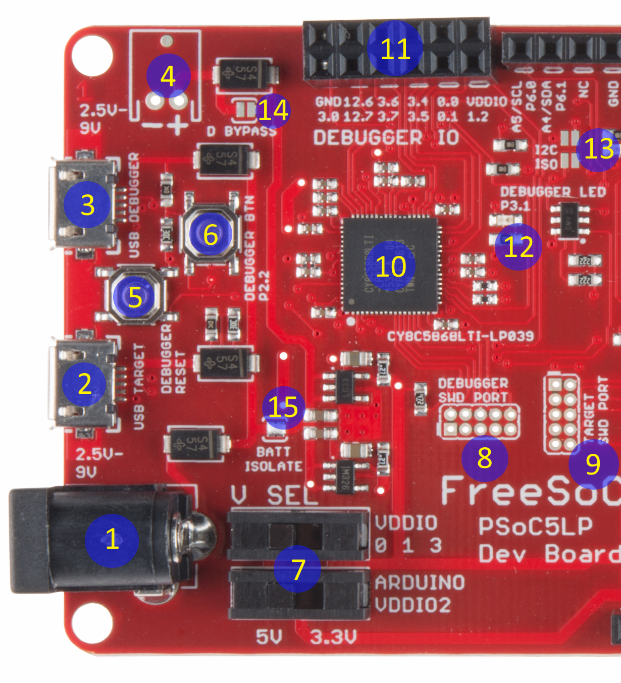
14. Battery Supply Diode Bypass – If you populate the 2.5mm JST connector and run the FreeSoC2 off of a
LiPo battery, you may find the ~0.5V drop across the diode which ORs the battery supply into the main
supply rail. This jumper may be closed with a blob of solder to bypass that diode.
Caution: if you close this jumper but fail to open the “BATT ISOLATE” jumper (item 15), plugging the
board into USB power may cause damage to your battery or even a fire as the 5V USB supply shorts
to the LiPo battery output.
15. Battery Isolate jumper – Whenever you close the “D BYPASS” jumper (item 14), this jumper must be
opened, to avoid risk of damage to the battery or fire.
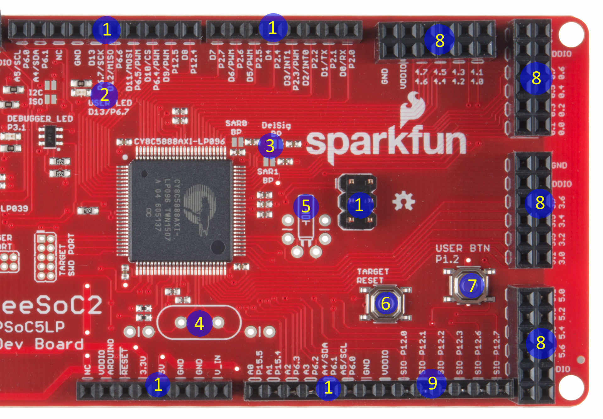
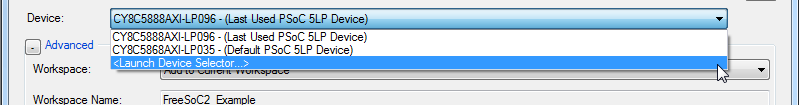
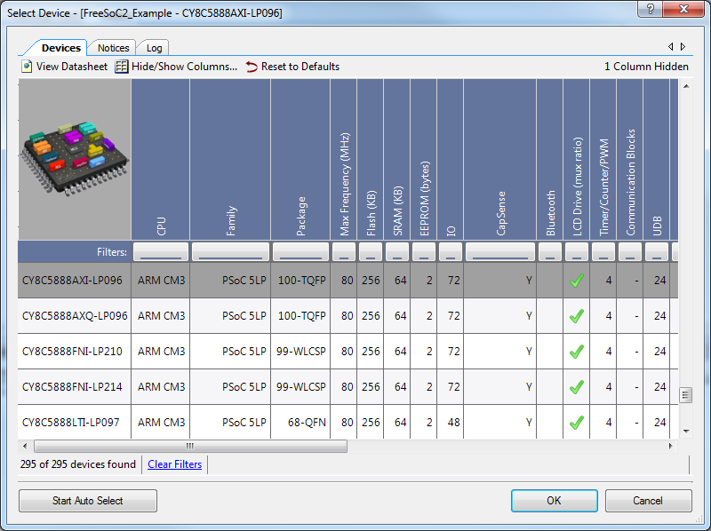
The right half of the board contains the target IC (a CY8C5888AXI-LP096) and the associated headers.
1. Arduino Uno R3-type headers – For the most part, these headers are completely compatible with the Uno
R3 board. The only exception is the VREF pin, normally located between the I C pins and the ground above
D13, is no-connect for this board.
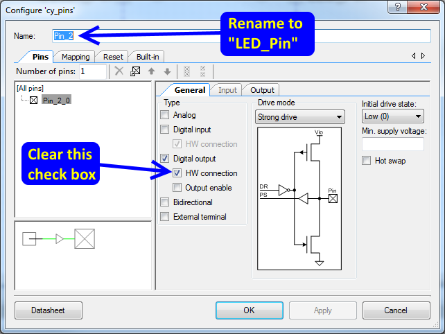
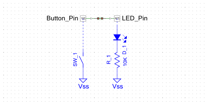
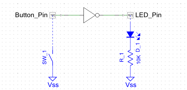
2. Target user LED – Tied to port 6, pin 7, which corresponds to D13 on the Arduino mapped headers.
3. ADC reference bypass capacitor jumpers – These jumpers allow you to add a 100nF capacitor to three of
the PSoC part’s pins, to provide a bypass for ADC voltage references to increase the reference’s accuracy.
4. High-frequency crystal footprint – if you need better accuracy than can be achieved by the onboard
oscillator, you may add a standard HC/49 crystal here.
5. Low-frequency crystal fooprint – if you want to implement an RTC, you may add a 32.768kHz clock crystal
here.
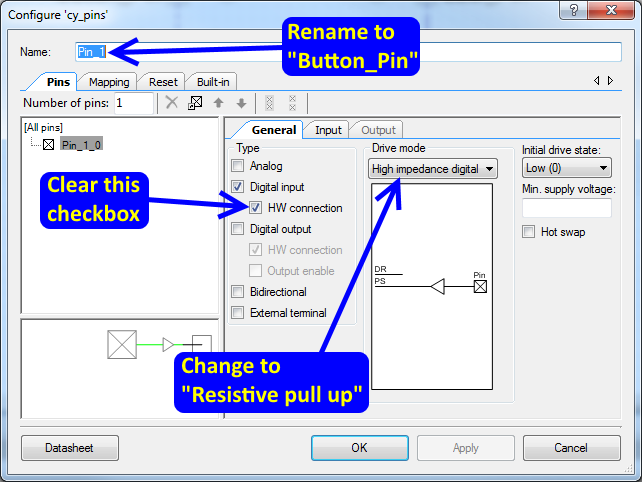
6. Target IC reset button – This button resets only the target IC.
7. Target IC user button – This button can be mapped to any purpose within the application; the button pulls
down to ground and is not tied to any other header.
8. Additional IO headers – These 2x6 headers are all additional I/O, and their voltage level (along with the
voltage present on the VDDIO pins of those headers) is controlled by the top VDDIO set switch on the left
end of the board and can be set to either 3.3V or 5V.
9. SIO pins – These six pins are special in that they can be connected to a signal voltage that is higher than
their nominal I/O voltage. They can, of course, be used normally as well. This allows these pins to be 5V
tolerant when the rest of the IO pins are running at 3.3V.
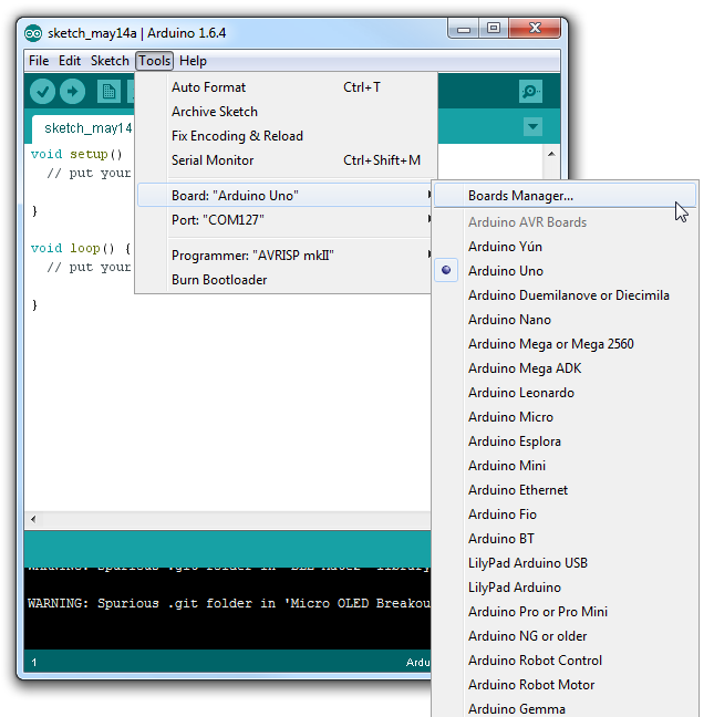
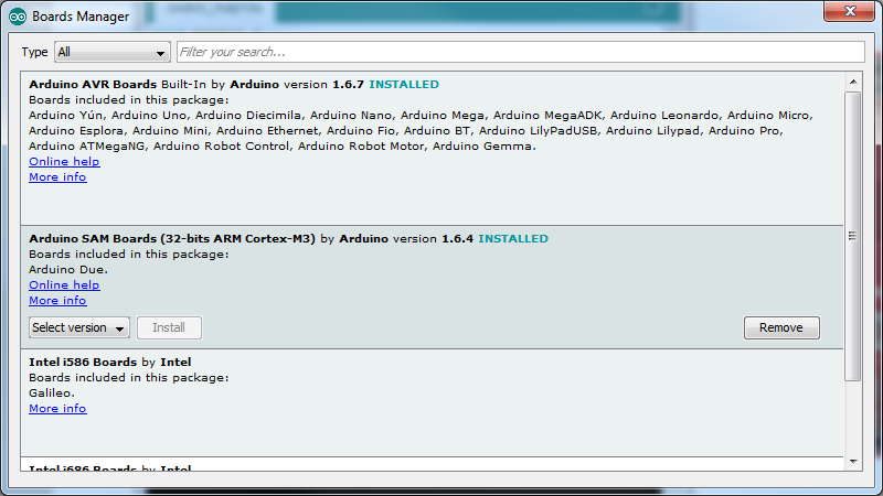
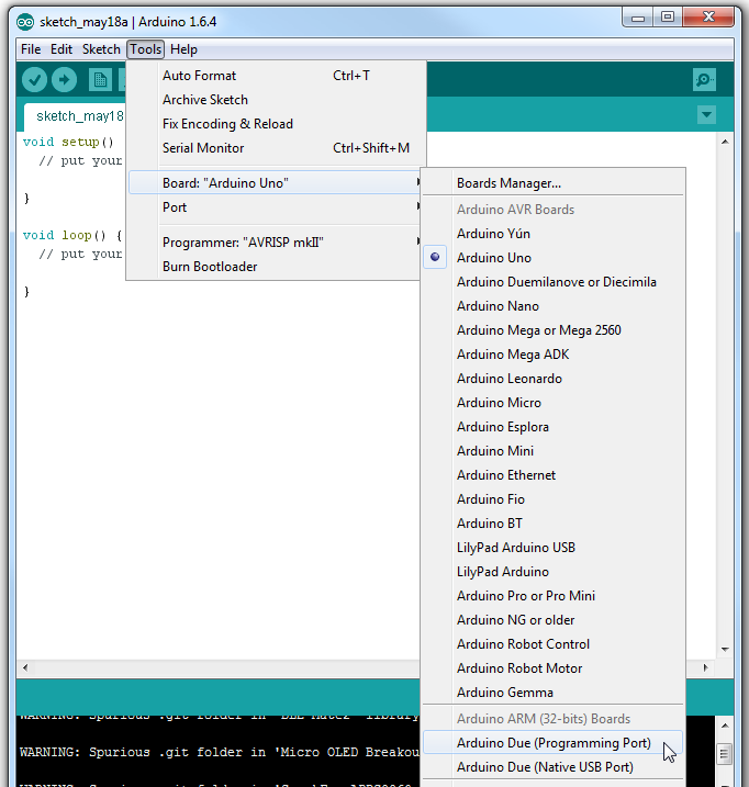
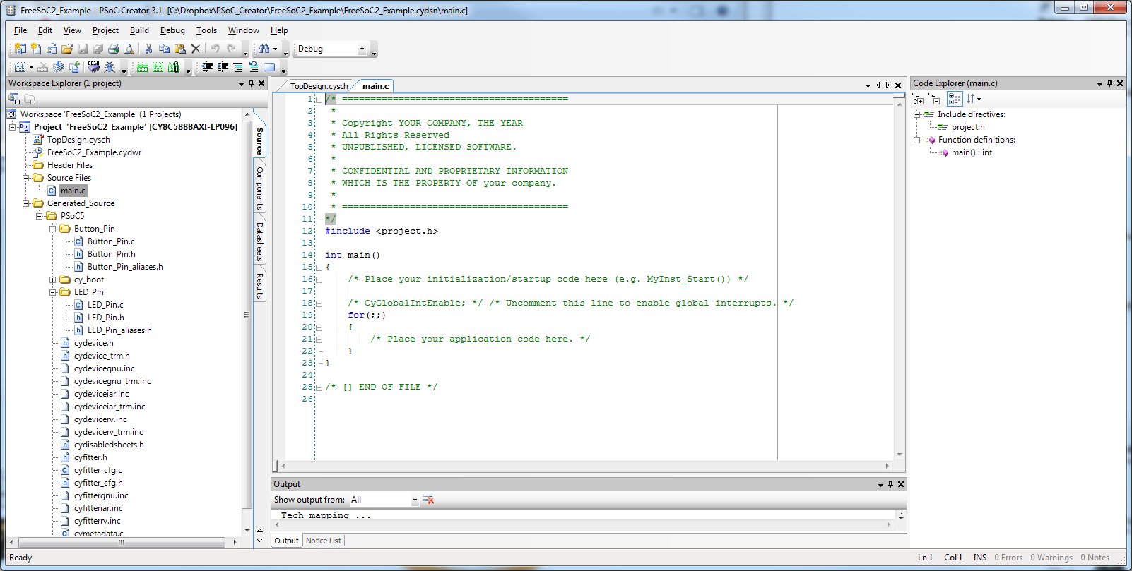
Using the Arduino IDE
2
2


 Technical document")


