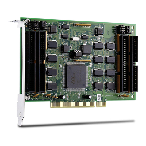
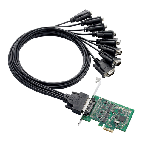
SpinCore Technologies PulseBlasterESR-PRO SP4B User manual

PulseBlasterESR-PRO™
(PCI Boards SP4B, SP18A, and SP19)
(USB Enclosure System SP45)
O ner’s Manual
SpinCore Technologies, Inc.
http:// .spincore.com

PulseBlasterESR-PRO
Congratulations and thank you for choosing a design from SpinCore
Technologies, Inc.
We appreciate your business!
At SpinCore, e aim to fully support the needs of our customers. If you
are in need of assistance, please contact us and e ill strive to
provide the necessary support.
© 2000-2019 SpinCore Technologies, nc. All rights reserved.
SpinCore Technologies, nc. reserves the right to make changes to the product(s) or information herein without notice.
PulseBlasterESR™, PulseBlaster™, SpinCore, and the SpinCore Technologies, nc. logos are trademarks of SpinCore Technologies, nc.
All other trademarks are the property of their respective owners.
SpinCore Technologies, nc. makes every effort to verify the correct operation of the equipment. This equipment version is not intended
for use in a system in which the failure of a SpinCore device will threaten the safety of equipment or person(s).
http://www.spincore.com 2 2019/09/26

PulseBlasterESR-PRO
Table of Contents
I. Introduction .................................................................................................. 5
Product Overvie .................................................................................................................... 5
Board Architecture .................................................................................................................. 6
Block Diagram ........................................................................................................... 6
Output Signals ........................................................................................................... 6
Timing Characteristics ............................................................................................... 7
Instruction Set ............................................................................................................ 7
External Triggering ..................................................................................................... 7
Summary .................................................................................................................... 7
Specifications ........................................................................................................................... 8
TTL Speci ications ..................................................................................................... 8
Pulse Parameters (using 500 MHz clock requency) ................................................ 8
Pulse Program Control Flow (Common) .................................................................... 8
II. Installation ................................................................................................... 9
Installing the PulseBlasterESR-PRO ....................................................................................... 9
III. Programming the PulseBlasterESR-PRO .............................................. 10
The PulseBlaster Interpreter .................................................................................................. 10
LabVIEW Extensions .............................................................................................................. 11
C/C++ Programming ............................................................................................................... 12
Using C Functions to Program the PulseBlasterESR-PRO ................................................. 14
Example Use o C Functions ................................................................................... 16
IV. Connecting to the PulseBlasterESR-PRO ............................................. 17
Connector Information for PulseBlasterESR-PRO Boards .................................................. 17
Connector Locations or the SP4B board ................................................................ 17
BNC Headers ........................................................................................................... 17
IDC Headers or SP4B and SP18A ......................................................................... 18
HWTrig/Reset Header or SP4B .............................................................................. 20
Connector Locations or the SP18A board .............................................................. 21
SMA Headers or SP18A ......................................................................................... 21
HW_Trig/Reset Header or SP18A and SP19 ......................................................... 21
Connector Locations or the SP19 board ................................................................ 23
http://www.spincore.com 3 2019/09/26

PulseBlasterESR-PRO
SMA Headers or SP19 ............................................................................................ 23
IDC Headers or SP19 ............................................................................................. 23
Clock Oscillator Header ......................................................................................................... 24
Connector Information for 2U BNC Rackmount Enclosure ................................................. 25
Connectors or 2U BNC Rackmount Enclosure ..................................................... 25
DB9 Connector (Trig/Res/Stat) or 2U BNC Rackmount Enclosure ........................ 25
Appendix I: Controlling the PulseBlasterESR-PRO ith SpinAPI ............ 27
Instruction Set Architecture ................................................................................................... 27
Machine-Word De inition ......................................................................................... 27
Breakdown o 80-bit Instruction Word ..................................................................... 27
About SpinAPI ......................................................................................................................... 31
Related Products and Accessories ............................................................. 32
Contact Information ...................................................................................... 35
Document Information .................................................................................. 35
http://www.spincore.com 4 2019/09/26

PulseBlasterESR-PRO
I. Introduction
Product Overvie
The PulseBlasterESR-PRO™ is a high-speed, intelligent pulse/pattern/delay generator designed for
outputting precisely timed TTL patterns. The intelligence of the PulseBlasterESR-PRO comes from an
embedded microprogrammed controller core nicknamed the PulseBlaster™. The controller is able to execute
instructions that allow it to control program flow much like a general purpose microcontroller. The speed of
the PulseBlasterESR-PRO comes from a maximum available clock of 500 MHz.
The PulseBlasterESR-PRO’s microprogrammed controller core is different from the general-purpose
microcontroller in that it contains a set of highly optimized instructions developed specifically for timing and
control applications. A unique and distinguishing feature of the PulseBlasterESR-PRO processor is that the
execution time for instructions is user programmable. This feature makes the PulseBlasterESR-PRO
processor capable of executing complex timing patterns at greatly varying update rates, ranging from
nanoseconds to months, with a constant setting accuracy of just one clock period.
http://www.spincore.com 5 2019/09/26

PulseBlasterESR-PRO
Board Architecture
Block Diagram
Figure 1 presents the general architecture of the PulseBlasterESR-PRO system. The major building
blocks are the SRAM memory, the PulseBlaster core, the integrated bus controller ( BC), the counter, and
the output buffers. The entire logic design, including the SRAM memory and output buffers, is contained
on a single silicon chip, making it a System-on-a-Chip design. User control to the system is provided
through the BC over the PC bus.
Output Signals
The PulseBlasterESR-PRO allows for 21 digital output signal lines. On the PC boards, all 21 signal
lines are routed to two sets of 26-pin DC on-board connectors. The first four output bits are also routed
to four bracket mounted BNC connectors. On the USB system, all 21 signal lines are routed to 21 BNC
connectors. The output signals are impedance matched to 50 ohm.
The 21 individually controlled digital output bits comply with the 3.3V TTL-levels’ standard, and are
capable of delivering 25 mA per bit/channel. Keep in mind that this is sufficient to provide a signal to a
132 ohm load, but if more current is necessary beyond this, the individual bits/channels can be driven in
parallel.
http://www.spincore.com 6 2019/09/26
Figure 1: PulseBlasterESR-PRO Board Architecture. The clock oscillator signal is derived
from an on-chip PLL circuit typically using a 50 MHz on-board reference clock.

PulseBlasterESR-PRO
Timing Characteristics
The PulseBlaster core's timing controller accepts an external (on-board) crystal oscillator of 50 MHz.
The input frequency is internally multiplied. The PulseBlasterESR-PRO is available with 4 different
internal clock frequencies: 250 MHz, 300 MHz, 400 MHz, and 500 MHz. The innovative architecture of
the timing controller allows the processing of either simple timing instructions (with delays of up to 232
clock cycles or 8.59 s at 500 MHz), or double-length timing instructions (up to 252 clock cycles long – over
100 days at 500 MHz!). Regardless of the type of timing instruction, the timing resolution remains
constant for any delay – just one clock period (e.g., 2 ns at 500 MHz).
The PulseBlaster core-timing controller has a very short minimum instruction time – only five clock
periods1. This translates to a 10 ns machine instruction time at 500 MHz. The PulseBlasterESR-PRO is
also capable of generating pulses on all outputs of lengths down to one clock cycle. For more information
on this feature, please see the Short Pulse Feature section in Appendix .
Instruction Set
The PulseBlaster core features a set of instructions for creating highly flexible pulse program flow
control. The micro-programmed controller allows for programs to include branches, subroutines, and
loops at up to 8 nested levels – all this to assist the user in creating dense pulse programs that cycle
through repetitious events, especially useful in numerous multidimensional spectroscopy and imaging
applications.
External Triggering
The PulseBlasterESR-PRO can be triggered and/or reset externally via dedicated hardware lines.
The two separate lines combine the convenience of triggering (e.g., in cardiac gating) with the safety of
the "stop/reset" line (firmware-dependent). The input pins for the trigger and reset are pulled to logical-
high on the board and can be activated by a low-voltage pulse (short to ground).
Summary
The PulseBlasterESR-PRO is a versatile, high-performance pulse/pattern TTL signal generator
operating at speeds of up to 500 MHz and capable of generating pulses ranging from 2 ns to 104 days
per instruction at intervals ranging from 10 ns to 8.59 s per instruction (using a 500 MHz clock signal). t
can accommodate pulse programs with highly flexible control commands of up to 4096 instruction words.
ts high-current output logic bits are independently controlled with an unterminated output voltage of 3.3 V.
1NOTE: For PulseBlasterESR-PRO-500 design 17-11, instructions with CONT NE, JSR, RTS and LONG_DELAY OpCodes, require a
minimum instruction time of at least 6 clock-cycles (12.0 ns). For PulseBlasterESR-PRO-400 design 9-18, the minimum instruction time
is 7 clock-cycles (17.5 ns).
http://www.spincore.com 7 2019/09/26

PulseBlasterESR-PRO
Specifications
TTL Speci ications
21 individually controlled digital output lines (LVTTL levels, 3.3 V logical “one” unterminated)
4 bracket mounted BNC connectors, impedance matched to 50 ohm, for board
24 BNC connectors for rackmount system, 21 of which are independently controlled output
channels
Variable pulses/delays for every TTL line
25 mA output current per TTL line
Pulse Parameters (using 500 MHz clock requency)
2 ns shortest pulse
10 ns shortest interval1
104 days longest pulse/interval (using the long delay instruction)
2 ns pulse/interval resolution
4096 instructions
External triggering and reset – 3.3V LVTTL levels
Pulse Program Control Flow (Common)
Loops, nested 8 levels deep
20 bit loop counters (max. 1,048,576 repetitions)
Subroutines, nested 8 levels deep
Wait for trigger – 8 clock cycle latency (16ns at 500 MHz), adjustable to 0.89 seconds in duration
15 MHz max. re-triggering frequency
1NOTE: For PulseBlasterESR-PRO-500 design 17-11, instructions with CONT NE, JSR, RTS and LONG_DELAY OpCodes, require a
minimum instruction time of at least 6 clock-cycles (12.0 ns). For PulseBlasterESR-PRO-400 design 9-18, the minimum instruction time
is 7 clock-cycles (17.5 ns).
http://www.spincore.com 8 2019/09/26

PulseBlasterESR-PRO
II. Installation
Installing the PulseBlasterESR-PRO
Whenever installing or uninstalling the PulseBlasterESR-PRO, always have it disconnected from the
computer initially. Uninstall any previous version of SpinAP .
1. nstall the latest version of SpinAP found at: http://www.spincore.com/support/spinapi/ .
•SpinAP is a custom Application Programming nterface developed by SpinCore Technologies,
nc. for use with the PulseBlasterESR-PRO and most of SpinCore's other products. t can be
utilized using C/C++ or graphically using the options in the next section below. The AP will also
install the necessary drivers.
2. Shut down the computer, unplug the power cord.
3. Connect the product to the computer.
a) For the PC : nsert the PulseBlasterESR-PRO card into an available PC slot and fasten the PC
bracket securely with a screw.
b) For the USB system: Plug one end of the USB cable into the PulseBlasterESR-PRO-USB-RM
and the other end into the host computer. Next, power the rackmount system.
4. Plug the PC power cord back in, turn on the computer and follow the installation prompts.
5. The simplest way to test whether the device has been installed properly and can be controlled as
intended is to run a simple test program. These example files can be found in the SpinAP package.
6. To open the SpinAP package on a Windows 10 PC, simply click the Window Start icon, and scroll
down to find and open the "spincore" folder. Example .exe files and their C source code can be found
in the folder /SpinAP /examples. From there, you may select the “PulseBlasterESR-PRO” folder and
run all .exe programs to test your PulseBlaster.
http://www.spincore.com 9 2019/09/26

PulseBlasterESR-PRO
III. Programming the PulseBlasterESR-PRO
SpinCore Technologies nc. is dedicated to providing an easy and efficient method of programming your
board. Various control methods available are detailed below, making PulseBlaster products flexible for any
number of applications.
Special consideration of the ESR-PRO Short Pulse feature must be taken when programming or
operating this board. For signals of instruction time greater than 10 ns, the Short Pulse feature must be
disabled by setting output bits 21-23 to H GH at all times. For more information, see Appendix .
The PulseBlaster Interpreter
The PulseBlasterESR-PRO can be programmed using PulseBlaster Interpreter, which is a free
programming utility provided by SpinCore for writing pulse programs. This easy-to-use editor allows you to
create, edit, save, and run your pulse sequence. Figure 2, below, shows the PulseBlaster nterpreter being
used with an example program.
http://www.spincore.com 10 2019/09/26
Figure 2: Graphical nterface of PulseBlaster nterpreter. The example shown
creates a pulse that toggles all TTL bits on for 100 ms, then off for 500 ms, and
repeats.

PulseBlasterESR-PRO
The PulseBlaster nterpreter is available as part of the SpinCore driver suite, and will be automatically
installed during the setup process (setup process is described in Section . nstallation). For convenience, a
shortcut to the PulseBlaster nterpreter will be added to your desktop. For more information on programming
using the PulseBlaster nterpreter, see the manual located at http://www.spincore.com/support/SPB /Doc/.
LabVIEW Extensions
The SpinCore PulseBlaster LabV EW Extensions (PBLV) provide the ability to program and control the
functionality of PulseBlaster boards using the simple National nstruments (N ) LabV EW graphical
programming interface. The package contains basic subV s that can be used to include PulseBlaster
interaction from your own LabV EW programs, as well as some complete example V s. Additionally, all of the
examples are available as stand-alone applications to control.
http://www.spincore.com 11 2019/09/26
Figure 3: Example of PulseBlaster LabV EW
Extensions User nterface.

PulseBlasterESR-PRO
There are two versions of the LabV EW extensions available free of charge on our website. The first is
for those who do not have LabV EW or who are not familiar with LabV EW programming. This option is a
stand-alone GU (see Figure 3 above) that comes in executable form and utilizes the LabV EW runtime
environment. The second is for those who have LabV EW and would like to make a custom interface for the
PulseBlasterESR-PRO. For more information and downloads please visit:
http://www.spincore.com/support/PBLV/
C/C++ Programming
The most dynamic and flexible way to program the PulseBlasterESR-PRO board is with C/C++ using the
SpinAP package. The GU based approaches to programming the board are designed for simplicity so they
can be used by someone with no programming experience.
While GU 's are easier to use, coding in C/C++ allows you to better utilize the various features of the
board and, in some cases, it may be easier to copy and paste lines of code than to make 100 instructions on
a GU . The instructions to compile on Windows can be found at
http://www.spincore.com/support/spinapi/Windows_Help.shtml. After configuring the compiler, changing one
of our example programs and recompiling the executable file for use with your PulseBlasterESR-PRO board
is as easy as clicking “Rebuild All” (see Figure 4 below).
http://www.spincore.com 12 2019/09/26
Figure 4: Compiling a C program to run the PulseBlasterESR-PRO board is easy!

PulseBlasterESR-PRO
Making changes to an example program requires understanding of only a few lines of code. The
following C code example generates a 50% duty cycle square wave with a 400.0 ms period.
A breakdown of the previous C code segment is as follows:
• Line 1: nitialize communication with the selected board. This must be called before any other
functions that communicate with the board.
• Line 2: Set the internal block clock frequency (in MHz). This must be called to insure proper timings
in the pulse program.
• Lines 7-10: Programs the board's pulse program memory.
◦ Line 7: pb_start_programming (PULSE_PROGRAM) must be called before using the
pb_inst(..) function.
◦ Line 8, instruction 1: Turn on bit 0 for 200.0 ms then continue to the next instruction. The
address of this instruction is stored in the “start” variable.
▪ Note: I the output is high or more than 5 clock cycles, it is necessary to turn o the Short
Pulse eature by settings bits 21-23 o the lag bits to “111.” This can be easily accomplished
by using the C-macro “ON” de ined in “spinapi.h.”
◦ Line 9, instruction 2: All bits off for 200.0 ms, then branch to “start.”
◦ Line 10: pb_stop_programming() must be called before calling any other SpinAP functions.
• Line 12: Start the board executing the Pulse Program.
• Line 13: Close communication with the board (Pulse Program execution will continue).
http://www.spincore.com 13 2019/09/26
1: pb_init(); /*Initialize communication with the board*/
2: pb_core_clock (CL CK); /*Set the internal clock frequency value – this
3: will be either 250, 300, 400, or 500 MHz
4: depending on your product */
5:
6: /*Start programming the Pulse Program*/
7: pb_start_programming (PULSE_PR GRAM);
8: start=pb_inst( N|0x01, C NTINUE, 0, 200.0*ms); /*Bit 0 on, 200ms*/
9: pb_inst(0x00, BRANCH, start, 200.0*ms);/*All bits off, 200ms*/
10: pb_stop_programming();
11:
12: pb_start(); /*Start the board executing*/
13: pb_close(); /*Close the communication with the board*/

PulseBlasterESR-PRO
Using C Functions to Program the PulseBlasterESR-PRO
A series of functions have been written to control the board and facilitate the construction of pulse
program instructions. t should be noted that the pb_inst C function accepts any delay value greater than 17
ns. Since the clock period is 3.3 ns for a 300 MHz clock, values which are not integer multiples of the clock
will be rounded to the closest integer multiple.
n order to use these functions, the DLL (spinapi.dll), the library file (libspinapi.a for MinGW, spinapilibgcc
for Borland, and spinapi.lib for MSVC), and the header file (spinapi.h), must be in the working directory of your
C compiler2.
int pb_init();
nitializes the PulseBlasterESR-PRO board. Needs to be called before calling any functions using the
device. t returns a 0 on success or a negative number on an error.
int pb_close();
Releases the PulseBlasterESR-PRO board. Needs to be called as last command in pulse program.
t returns a 0 on success or a negative number on an error.
void pb_core_clock(double clock_freq);
Used to set the clock frequency of the board. The variable clock_frequency is specified in MHz
when no units are entered. Valid units are MHz, kHz, and Hz. The default clock value is 400 MHz.
You only need to call this function if you are not using a 400 board.
int pb_start_programming(int device);
Used to initialize the system to receive programming information. t accepts a parameter referencing
the target for the instructions. The only valid value for device is PULSE_PROGRAM. t returns a 0 on
success or a negative number on an error.
2 These functions and ibrary fi es have been generated and tested with MinGW (www.mingw.com), Bor and 5.5 (www.bor and.com), MS
Visua Studio 2003 (msdn.microsoft.com) compi ers.
http://www.spincore.com 14 2019/09/26

PulseBlasterESR-PRO
int pb_inst(int flags, int inst, int inst_data, double length);
Used to send one instruction of the pulse program. Should only be called after
pb_start_programming(PULSE_PROGRAM) has been called. t returns a negative number on an
error, or the instruction number upon success. f the function returns –99, an invalid parameter was
passed to the function. nstructions are numbered starting at 0.
int flags – determines state of each TTL output bit. Valid values are 0x000000 to 0x1FFFFF. For
example, 0x000010 would correspond to bit 4 being on, and all other bits being off.
int inst – determines which type of instruction is to be executed. Please see Table 7 for details.
int inst_data – data to be used with the previous inst field. Please see Table 7 for details.
double length – duration of this pulse program instruction, specified in nanoseconds (ns),
microseconds (us) or milliseconds (ms).
The largest value for the delay field of the pb_inst is 8589 ms (using a 500 MHz clock).
For longer delays, use the L NG_DELAY instruction (see Table 7). The maximum value for
the data field of the L NG_DELAY is 1048576. Even longer delays can be achieved using
the L NG_DELAY instruction inside of a loop.
int pb_stop_programming();
Used to tell that programming the board is complete. Board execution cannot start until this
command is received. t returns a 0 on success or a negative number on an error.
int pb_start();
Once board has been programmed, this instruction will start execution of pulse program. t returns a
0 on success or a negative number on an error.
int pb_stop();
Stop the Pulse Program execution. TTL outputs will either remain in their last state or return to zero,
depending on the firmware version of the board. t returns a 0 on success or a negative number on
an error.
http://www.spincore.com 15 2019/09/26

PulseBlasterESR-PRO
There are currently six example C programs available with the SpinAP package in the PulseBlasterESR-
PRO directory.
Example Use o C Functions
http://www.spincore.com 16 2019/09/26
#include <stdio.h>
#include <stdlib.h>
#define PBESRPR
#include "spinapi.h"
#define CL CK 400.0 // PulseBlaster core clock rate
int main (int argc, char **argv)
{
int start;
printf ("Copyright (c) 2010 SpinCore Technologies, Inc.\n\n");
printf("Using SpinAPI library version %s\n", pb_get_version());
if (pb_init () != 0) {
printf ("Error initializing board: %s\n", pb_get_error());
system("pause");
}
// Tell driver what clock frequency the board uses
pb_core_clock(CL CK);
// Prepare the board to receive pulse program instructions
pb_start_programming(PULSE_PR GRAM);
// Instruction 0 - Continue to instruction 1 in 20ns. The lower 4 bits
// (all BNC connectors) will be driving high. For PBESR-PR boards,
// or-ing THREE_PERI D with the flags causes a 3 period short
// pulse to be used.
start = pb_inst(THREE_PERI D | 0xF, C NTINUE, 0, 20.0 * ns);
// Instruction 1 - Continue to instruction 2 in 40ns
// The BNC1-3 will be driving high the entire 40ns.
pb_inst( N | 0xE, C NTINUE, 0, 40.0 * ns);
// Instruction 2 - Branch to "start" (Instruction 0) in 40ns
// utputs are off
pb_inst(0, BRANCH, start, 40.0 * ns);
pb_stop_programming(); // Finished sending instructions
pb_reset();
pb_start(); // Trigger the pulse program
// End communication with PulseBlasterESR-PR board. The pulse program
// will continue to run even after this is called.
pb_close();
return 0;
}

PulseBlasterESR-PRO
IV. Connecting to the PulseBlasterESR-PRO
The PulseBlasterESR-PRO functionality is available on SP4B, SP18A , SP19 boards, and SP45 USB
rackmount system. The connectors for the PulseBlasterESR-PRO boards and USB rackmount system are
explained below in their respective sections.
Connector Information for PulseBlasterESR-PRO Boards
On the PC boards (SP4B, SP18A, SP19), there are three main connector banks: the BNC headers, the
DC headers, and the Trigger/Reset header. Additionally, the SP18A and SP19 boards offer SMA headers.
Please refer to the sections below for detailed connector information.
Connector Locations or the SP4B board
Figure 5 shows the connector locations for SP4B boards.
BNC Headers
The four BNC headers provide access to the least significant four bits of the flag word. Bit 3 is
connected to the output farthest from the PC connector, and Bit 0 is connected to the connector closest to the
PC connector. Please note that the BNC connectors have the same configuration for all board models.
f using a high input impedance oscilloscope to monitor the PulseBlasterESR-PRO's output via the
BNC connectors, place a resistor that matches the characteristic impedance of the transmission line in
parallel with the coaxial transmission line at the oscilloscope input (e.g., a 50 Ω resistor with a 50 Ω
transmission line, see Figures 6 and 7 below). When using an oscilloscope with an adjustable bandwidth, set
the bandwidth to as large as possible. Failure to do so may yield inaccurate readouts on the oscilloscope.
http://www.spincore.com 17 2019/09/26
Figure 5: Connector locations for SP4B. The SP4B board is shown on the
first page of this manual, left picture.
BNC3
BNC2
BNC1
BNC0
Flag0...11 Out Flag12..23 Out Flag24..35 Out
HWTR G/RESET

PulseBlasterESR-PRO
IDC Headers or SP4B and SP18A
There are three DC headers on SP4B and SP18 boards, which provide access to all digital 21
outputs as well as the status bits. These are labeled on the board as Flag0..11 Out, Flag12..23 Out and
Flag24..35 Out. On each DC header, the top row of pins (14-26) are grounds, and the signals are
carried on pins 1-13. The recommended mating connector for DC header can be obtained through Digi-
Key Part Number: CKR26G-ND.
http://www.spincore.com 18 2019/09/26
Figure 8: DC header Pin-Out.
14 15 16 17 18 19 20 21 22 23 24 25 26
1 2 3 4 5 6 7 8 9 10 11 12 13
Figure 6: Left: BNC T-Adapter and Right: BNC 50 Ohm resistor.
Figure 7: BNC T-Adapter on the oscilloscope with coaxial
transmission line connected on the left and BNC 50 Ohm resistor
connected on the right, to terminate the line.

PulseBlasterESR-PRO
Each pin on an DC header corresponds to a bit in the flag field of an instruction. The association
between bits and pins are shown in the table below.
Alternatively, the DC headers can be connected to DC-MMCX adapter boards (Figure 20) which
allow the use of MMCX cables. This enables the individual bits of the PulseBlasterESR-PRO to be more
easily accessed. Pin 1 on the MMCX adapters can be identified with a square pin.
The Status pins are set or cleared based on the state of the PulseBlasterESR-PRO. The pins are
located on DC header Flag24...35, from pin 1 to pin 4. The status pins are defined as follows:
Status Pins Description
• Stopped – Driven high when the PulseBlasterESR-PRO has encountered a STOP OpCode during
program execution and has entered a stopped state.
• Reset – Driven low when the PulseBlasterESR-PRO is in a RESET state. The device must be
reprogrammed before code execution can begin again.
• Running – Driven high when the PulseBlasterESR-PRO is executing a program. The pin is driven
low when the PulseBlasterESR-PRO enters either a reset or idle state.
• Waiting – Driven high when the PulseBlasterESR-PRO has encountered a WA T OpCode, and is
waiting for the next trigger (either hardware or software) to resume operation.
Note that it is also possible to read the status bits via software by using the pb_read_status() function.
Please see http://www.spincore.com/CD/spinapi/spinapi_reference/ for details.
http://www.spincore.com 19 2019/09/26
Pin Assignments
Pin# Flag0..11 Flag12..23 Flag24..35
1 Bit 0 Bit 12 Stopped
2 Bit 1 Bit 13 Reset
3 Bit 2 Bit 14 Running
4 Bit 3 Bit 15 Waiting
5 Bit 4 Bit 16 Unused
6 Bit 5 Bit 17 Unused
7 Bit 6 Bit 18 Unused
8 Bit 7 Bit 19 Unused
9 Bit 8 Bit 20 Unused
10 Bit 9 Bit 21 Unused
11 Bit 10 Bit 22 Unused
12 Bit 11 Bit 23 Unused
13 Unused Unused Unused
14-26 Ground Ground Ground
Table 1: DC connector pin outs.

4 3
2 1
PulseBlasterESR-PRO
HWTrig/Reset Header or SP4B
This is an input connector, for hardware triggering (HW_Trigger) and hardware resetting (HW_Reset).
Pins 1 and 2 are the reset and trigger inputs, respectively, and pins 3 and 4 are grounds.
CAUTION: Applying voltages to the input pins that are greater than 3.3 V or less than 0 V will
damage the PulseBlasterESR-PRO.
HW_Trigger is pulled to logical-high voltage (3.3V) on the board. Pin 2 is active and pin 4 is the
corresponding ground. When a falling edge is detected (e.g., when shorting pins 2-4) and the program is
idle, code execution is triggered. f the program is idle due to a WA T OpCode, then the HW_Trigger will
cause the program to continue to the next instruction. f the program is idle due to a STOP OpCode or a
HW_Reset signal, then the HW_Trigger starts execution from the beginning of the program. When using
the STOP OpCode, a HW_Reset or software reset (pb_reset()) needs to be applied prior to the
HW_Trigger.
Figure 12 in HW_Trig/Reset Header for SP18A and SP19 shows an example of the HW_Trigger
signal.
HW_Reset is pulled to logical-high voltage (3.3V) on the board. Pin 1 is active and pin 3 is the
corresponding ground. t can be used to halt the execution of a program by pulling it low (e.g., by shorting
pins 1-3). When the signal is pulled low during the execution of a program, the controller resets itself
back to the beginning of the program. Program execution can be resumed by either a software start
command (pb_start()) or by a hardware trigger.
http://www.spincore.com 20 2019/09/26
Figure 9: HWTrig/Reset Header Pin-Out (SP4B).
This manual suits for next models
3
Table of contents
Other SpinCore Technologies PCI Card manuals
SpinCore Technologies
SpinCore Technologies RadioProcessor USB User manual
SpinCore Technologies
SpinCore Technologies RadioProcessor-G User manual
SpinCore Technologies
SpinCore Technologies ClockMaster CM2-100-PCI User manual
SpinCore Technologies
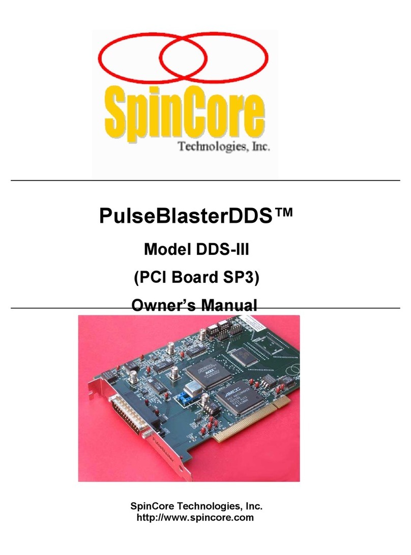
SpinCore Technologies PulseBlaster DDS-III User manual
SpinCore Technologies
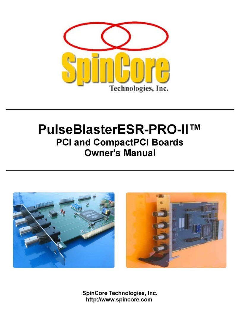
SpinCore Technologies PulseBlasterESR-PRO-II User manual
SpinCore Technologies
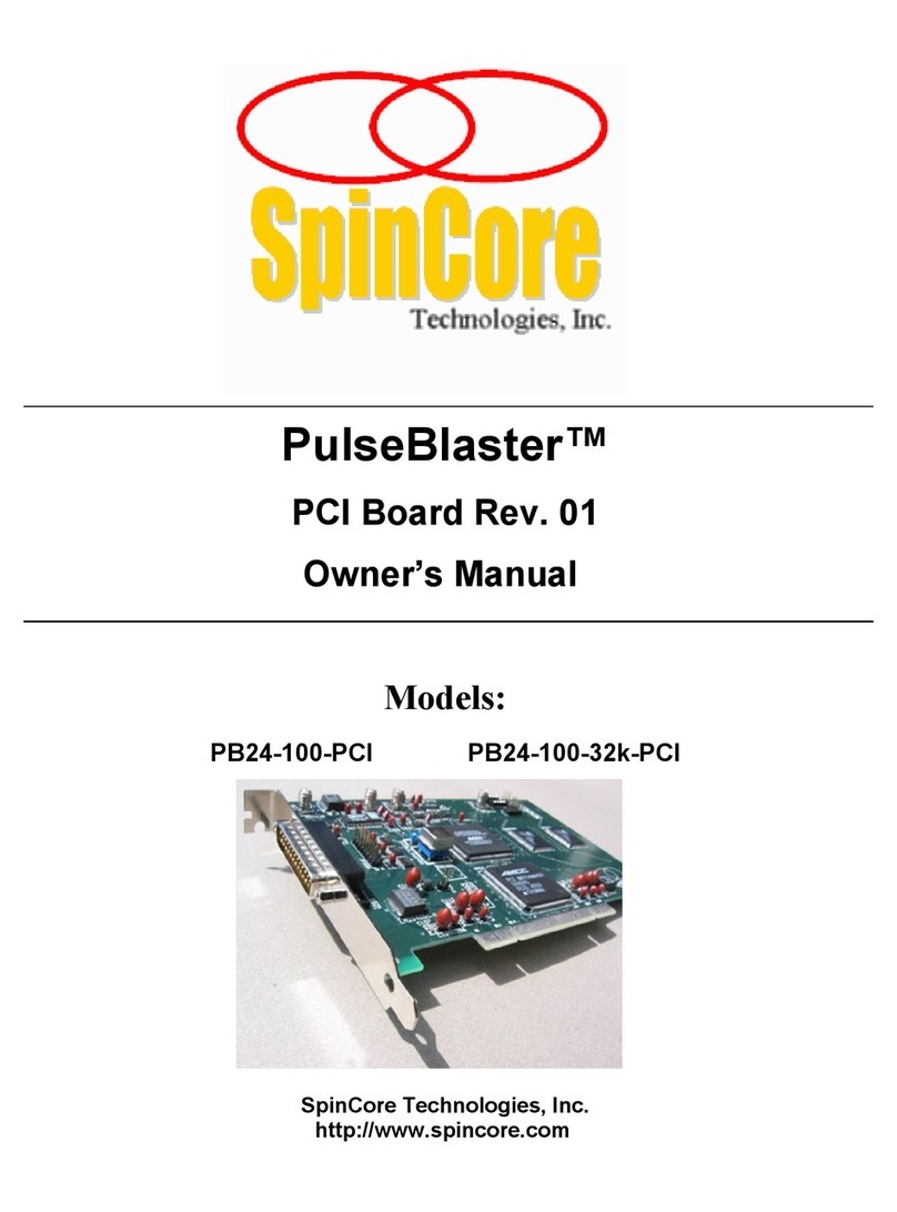
SpinCore Technologies PulseBlaster PB24-100-PCI User manual
