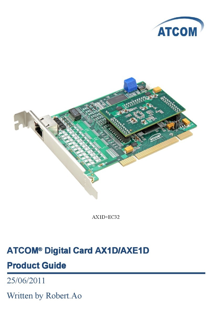
SpinCore Technologies PulseBlaster PB24-100-PCI User manual

PulseBlaster™
PCI Board Rev. 01
Owner’s Manual
Models:
PB24-100-PCI PB24-100-32k-PCI
S inCore Technologies, Inc.
htt ://www.s incore.com

PulseBlaster
Congratulations and thank you for choosing a design from
S inCore Technologies, Inc.
We a reciate your business!
At S inCore we aim to fully su ort the needs of our customers. If you
are in need of assistance, lease contact us and we will strive to rovide
the necessary su ort.
© 2000-2006 SpinCore Technologies, Inc. All rights reserved.
SpinCore Technologies, Inc. reserves the right to make changes to the product s) or information herein without notice.
PulseBlasterDDS™, PulseBlaster™, SpinCore, and the SpinCore Technologies, Inc. logos are trademarks of SpinCore Technologies,
Inc. All other trademarks are the property of their respective owners.
SpinCore Technologies, Inc. makes every effort to verify the correct operation of the equipment. This equipment version is not intended
for use in a system in which the failure of a SpinCore device will threaten the safety of equipment or person s).
http://www.spincore.com 5/19/2006
2

PulseBlaster
Table of Contents
I. Introduction................................................................................................. 5
Product Overview ......................................................................................................... 5
Board Architecture ....................................................................................................... 5
Block Diagram ......................................................................................................... 5
Output signals.......................................................................................................... 6
Timing characteristics............................................................................................... 6
Instruction set........................................................................................................... 6
External triggering ................................................................................................... 6
Summary.................................................................................................................. 6
S ecifications................................................................................................................ 7
TTL Specifications....................................................................................................
Pulse Parameters.....................................................................................................
Pulse Program Control Flow (Common)...................................................................
II. Installation................................................................................................... 8
Installing the PulseBlaster Driver ............................................................................... 8
III. Programming the PulseBlaster................................................................. 8
The PulseBlaster Inter reter........................................................................................ 8
IV. Connecting to the PulseBlaster Board.................................................... 9
Connector Information.................................................................................................. 9
DB-25 and JP300 - TTL Output Signal Bits............................................................. 9
Header JP100.......................................................................................................... 9
A endix I: Controlling the PulseBlaster with S ina i............................. 10
Instruction Set Architecture....................................................................................... 10
Machine-Word Definition........................................................................................ 10
Breakdown of 80-bit Instruction Word.................................................................... 10
About S ina i.............................................................................................................. 12
Using C Functions to Program the PulseBlaster..................................................... 12
Example Use of C Functions.................................................................................. 14
http://www.spincore.com 5/19/2006
3

PulseBlaster
A endix II: Sam le C Program.................................................................. 15
Contact Information...................................................................................... 17
http://www.spincore.com 5/19/2006
4

PulseBlaster
I. Introduction
Product Overview
The PulseBlaster device is an intelligent pulse/pattern generation unit. The intelligence of the
PulseBlaster comes from an imbedded microprogrammed controller core uPC). The controller is able to
execute instructions that allow it to control program flow. This means that the PulseBlaster understands
Operational Control Codes, Op Codes, and will execute them much the same way as a general-purpose
microprocessor does. The PulseBlaster’s microcontroller is different from the general-purpose
microprocessor in that it does not contain an arithmetic logic unit ALU) and is incapable of doing
mathematical or logical calculations. However, a unique and distinguishing feature of the PulseBlaster
processor is that the execution time of instructions is user programmable. This feature makes the
PulseBlaster processor capable of executing complex patterns at greatly varying update rates, ranging from
nanoseconds to years per single instruction, with a constant setting accuracy of just one clock period e.g., a
10 ns setting accuracy at a 100 MHz clock frequency).
Board Architecture
Block Diagram
Figure 1 presents the general architecture of the PulseBlaster system. The major building blocks are
the SRAM memory both internal and external to the processor), the microcontroller uPC), the integrated
bus controller IBC), the counter, and the output buffers. The entire logic design, excluding output buffers,
is contained on a single silicon chip, making it a System-on-a-Chip design. User control to the system is
provided through the integrated bus controlled over the PCI bus.
Figure 1: PulseBlaster board architecture
http://www.spincore.com 5/19/2006
5
PCI Bus

PulseBlaster
Output signals
The PulseBlaster comes with 24 digital output signal lines. The 24 individually controlled digital
TTL/CMOS) output bits are capable of delivering ±25 mA per bit and have an output voltage of 3.3V.
These signals are available on the PC bracket-mounted DB-25 connector 16 channels) and an on-board
IDC two-row header connector the remaining 8 channels).
Timing characteristics
PulseBlaster’s timing controller can accept either an internal on-board) crystal oscillator or an
external frequency source of up to 100 MHz. The innovative architecture of the timing controller allows
the processing of either simple timing instructions delays of up to 232 = 4,294,967,296 clock cycles), or
double-length timing instructions up to 252 clock cycles long – nearly 2 years with a 100 MHz clock!).
Regardless of the type of timing instruction, the timing resolution remains constant for any delay – just
one clock period e.g., 10 ns for a 100 MHz clock).
The core-timing controller has a very short minimum delay cycle – only five clock periods for internal
memory 512 words) models. This translates to a 50 ns pulse/delay/update with a 100 MHz clock. The
external memory models up to 32k words) have a nine clock-period minimum instruction cycle.
Instruction set
PulseBlaster’s design features a set of commands for highly flexible program flow control. The micro-
programmed controller allows for programs to include branches, subroutines, and loops at up to 8 nested
levels – all this to assist the user in creating dense pulse programs that cycle through repetitious events,
especially useful in numerous multidimensional spectroscopy and imaging applications.
External triggering
PulseBlaster can be triggered and/or reset externally via dedicated hardware lines. The two separate
lines combine the convenience of triggering e.g., in cardiac gating) with the safety of the "stop/reset" line.
The required control signals are “active low” or short to ground).
Summary
PulseBlaster is a versatile, high-performance pulse/pattern TTL signal generator operating at speeds
of up to 100 MHz and capable of generating pulses/delays/intervals ranging from 50 ns to over 2 years
per instruction. It can accommodate pulse programs with highly flexible control commands of up to 32k
program words. Its high-current output logic bits are independently controlled with a voltage of 3.3 V.
http://www.spincore.com 5/19/2006
6

PulseBlaster
S ecifications
TTL Specifications
•24 individually controlled digital output lines TTL levels)
•variable pulses/delays for every TTL line
•25 mA output current per TTL line
•output lines can be combined to increase the max. output current
Pulse Parameters
•50 ns shortest pulse/interval for 512 memory-words models at 100 MHz
•90 ns shortest pulse/interval for 32k memory words models at 100 MHz.
•2 years longest pulse/interval
•10 ns pulse/interval resolution at 100 MHz)
•32k instructions max. memory space 512 instructions for internal memory models)
•external triggering and reset – TTL levels
Pulse Program Control Flo (Common)
•loops, nested 8 levels deep
•20 bit loop counters max. 1,048,576 repetitions)
•subroutines, nested 8 levels deep
•wait for trigger – 8 clock cycle latency 80ns at 100 MHz), adjustable to 2 years in duration
•5 MHz max. re-triggering frequency\
http://www.spincore.com 5/19/2006
7

PulseBlaster
II. Installation
Installing the PulseBlaster Driver
The PulseBlaster uses the Spinapi driver and control library. The latest version of this driver can
bedownloaded from:
htt ://www. ulseblaster.com/CD/s ina i/
This URL contains both the driver as well as the most recent installation guide. Please refer to that document
for instructions on how to properly install the drivers.
III. Programming the PulseBlaster
The PulseBlaster Inter reter
The PulseBlaster board is now programmable via the PulseBlaster Interpreter, which is a free
programming utility provided by SpinCore for writing pulse programs. This easy-to-use editor allows you
create, edit, save and run your pulse sequence.
Figure 2: The PulseBlaster Interpreter
Please follow the link below for the most recent installation instructions and documentation:
htt ://www. ulseblaster.com/CD/s bi/
It is also possible to write pulse programs and control the PulseBlaster with C functions. For more information
on this, please see Appendix I.
http://www.spincore.com 5/19/2006
8

PulseBlaster
IV. Connecting to the PulseBlaster Board
Connector Information
DB-25 and JP300 - TTL Output Signal Bits
Outputs TTL signals generated by the user’s Program. Please consult the table below for bit
assignments.
DB-25 Pin Assignments JP300 Pin Assignments
Pin# Bit# Pin# Bit# Pin# Bit# Pin# Bit#
1 GND 14 GND 1 23 9 19
2 15 15 14 2 GND 10 GND
3 GND 16 13 3 22 11 18
4 12 17 GND 4 GND 12 GND
5 11 18 10 5 21 13 17
6 GND 19 9 6 GND 14 GND
7 8 20 GND 7 20 15 16
8 7 21 6 8 GND 16 GND
9 GND 22 5
10 4 23 GND
11 3 24 2
12 GND 25 1
13 0
Table 3: Output bits and signals of the PulseBlaster
Header JP100
This is an input connector, for hardware triggering HW_Trigger) and resetting HW_Reset).
HW_Trigger is pulled high by default, and pin 1 is active pin 2 = GND). When a falling edge is
detected e.g., when shorting pins 1-2), it initiates code execution. This trigger will also restart execution
of a program from the beginning of the code if it is detected after the design has reached an idle state.
The idle state could have been created either by reaching the STOP Op Code of a program, or by the
detection of the HW_Reset signal. When the WAIT Op Code is used in the pulse program, the
HW_Trigger will cause the program to continue to the next instruction.
HW_Reset is pulled high by default, and pin 3 is active pin 4 = GND). It can be used to halt the
execution of a program by pulling it low e.g., by shorting pins 3-4). When the signal is pulled low during
the execution of a program, the controller resets itself back to the beginning of the program. Program
execution can be resumed by either a software start command or by a hardware trigger.
http://www.spincore.com 5/19/2006
9

PulseBlaster
A endix I: Controlling the PulseBlaster with S ina i
Instruction Set Architecture
Machine-Word Definition
The PulseBlaster pulse timing and control processor implements an 80-bit wide Very Long Instruction
Word VLIW) architecture. The VLIW memory words have specific bits/fields dedicated to specific
purposes, and every word should be viewed as a single instruction of the micro-controller. The maximum
number of instructions that can be loaded to on-board memory is 32k. The execution time of instructions
can be varied and is under self) control by one of the fields of the instruction word – the shortest being
five clock cycles for 512 memory-word models) and the longest being 2^52 clock cycles. All instructions
have the same format and bit length, and all bit fields have to be filled. Figure 3 shows the fields and bit
definitions of the 80-bit instruction word.
Bit Definitions for the 80-bit Instruction Word (VLIW)
Output/Control Word | Data Field | OP Code | Delay Count
(24 bits) (20 bits) (4 bits) (32 bits)
Figure 3: Bit definitions of the 80-bit instruction/memory word
Breakdo n of 80-bit Instruction Word
The 80-bit VLIW is broken up into 4 sections
1. Output Pattern and Control Word - 24 bits
2. Data Field - 20 bits
3. OP Code - 4 bits
4. Delay Count - 32 bits
http://www.spincore.com 5/19/2006
10

PulseBlaster
Output Pattern and Control Word
Please refer to Table 1 for output pattern and control bit assignments of the 24-bit output/control word.
Bit
#
Bit # Function
23 Header JP300 pin 1 11 Output Connector DB25 pin 5
22 Header JP300 pin 3 10 Output Connector DB25 pin 18
21 Header JP300 pin 5 9 Output Connector DB25 pin 19
20 Header JP300 pin 7 8 Output Connector DB25 pin 7
19 Header JP300 pin 9 7 Output Connector DB25 pin 8
18 Header JP300 pin 11 6 Output Connector DB25 pin 21
17 Header JP300 pin 13 5 Output Connector DB25 pin 22
16 Header JP300 pin 15 4 Output Connector DB25 pin 10
15 Output Connector DB25 pin 2 3 Output Connector DB25 pin 11
14 Output Connector DB25 pin 15 2 Output Connector DB25 pin 24
13 Output Connector DB25 pin 16 1 Output Connector DB25 pin 25
12 Output Connector DB25 pin 4 0 Output Connector DB25 pin 13
Table 1: Output Pattern and Control Word Bits
Data Field and Op Code
Please refer to Table 2 for information on the available operational codes OpCode) and the associated
data field functions the data field's function is dependent on the Op Code)
Op Code # Inst Inst_data Function
0 CONTINUE Ignored Program execution continues to next
instruction
1 STOP Ignored
Stop execution of program *Note all TTL
values remain from previous instruction, and
analog outputs turn off)
2 LOOP
Number of desired loops. This
value must be greater than or
equal to 1.
Specify beginning of a loop. Execution
continues to next instruction. Data used to
specify number of loops
3 END_LOOP Address of beginning of loop
Specify end of a loop. Execution returns to
begging of loop and decrements loop
counter.
4 JSR Address of first subroutine
instruction
Program execution jumps to beginning of a
subroutine
5 RTS Ignored Program execution returns to instruction
after JSR was called
6 BRANCH Address of next instruction Program execution continues at specified
instruction
7 LONG_DELAY
Number of desired loops. This
value must be greater than or
equal to 2.
For long interval instructions. Data field
specifies a multiplier of the delay field.
Execution continues to next instruction
8 WAIT Ignored
Program execution stops and waits for
software or hardware trigger. Execution
continues to next instruction after receipt of
trigger. The latency is equal to the delay
value entered in the WAIT instruction line
plus a fixed delay of 6 clock cycles.
Table 2: Op Code and Data Field Description
http://www.spincore.com 5/19/2006
11

PulseBlaster
Delay Count
The value of the Delay Count field a 32-bit value) determines how long the current instruction should be
executed. The allowed minimum value of this field is 0x6 for the 32k memory models and 0x2 for the internal-
memory models. The timing controller has a fixed delay of three clock cycles and the value that one enters
into the Delay Count field should account for this inherent delay.
About S ina i
Spinapi is a control library which allows programs to be written to communicate with the PulseBlaster
board. The most straightforward way to interface with this library is with a C/C++ program, and the API
definitions are described in this context. However, virtually all programming languages and software
environments including software such as LabView and Matlab) provide mechanisms for accessing the
functionality of standard libraries such as Spinapi.
Please see the example programs for an an explanation of how to use Spinapi. A reference
document for the API is available online at:
http://www.pulseblaster.com/CD/spinapi/spinapi_reference/
Using C Functions to Program the PulseBlaster
A series of functions have been written to control the board and facilitate the construction of pulse
program instructions.
IIn order to use these functions, the DLL spinapi.dll), the library file libspinapi.a for mingw, spinapilibgcc
for borland, and spinapi.lib for msvc), the header file spinapi.h), must be in the working directory of your C
compiler1.
int pb_init();
Initializes PulseBlaster board. Needs to be called before calling any functions using the PulseBlaster.
Returns a negative number on an error or 0 on success.
int pb_close();
Releases PulseBlaster board. Needs to be called as last command in pulse program. Returns a
negative number on an error or 0 on success.
void set_clock(double clock_fre );
Used to set the clock frequency of the board. The variable clock_frequency is specified in MHz
when no units are entered. Valid units are MHz, kHz, and Hz. The default clock value is 50MHz.
You only need to call this function if you are not using a –50 board.
int start_programming(int device);
Used to initialize the system to receive programming information. It accepts a parameter referencing
the target for the instructions. The only alid value for device is PULSE_PROGRAM, It returns a 0 on
success or a negative number on an error.
1 These functions and ibrary fi es have been generated and tested with MinGW (www.mingw.com), Bor and 5.5 (www.bor and.com), MS
Visua Studio 2003 (msdn.microsoft.com) compi ers.
http://www.spincore.com 5/19/2006
12

PulseBlaster
int pb_inst(int flags, int inst, int inst_data, double length);
Used to send one instruction of the pulse program. Should only be called after
start_programming PULSE_PROGRAM) has been called. It returns a negative number on an error,
or the instruction number upon success. If the function returns –99, an invalid parameter was passed
to the function. Instructions are numbered starting at 0.
int flags – determines state of each TTL output bit. Valid values are 0x0 to 0x3FF. For example,
0x010 would correspond to bit 7 being on, and all other bits being off.
int inst – determines which type of instruction is to be executed. Please see Table 2 for details.
int inst_data – data to be used with the previous inst field. Please see Table 2 for details.
int length – duration of this pulse program instruction, specified in ns.
int stop_programming();
Used to tell that programming the board is complete. Board execution cannot start until this
command is received. It returns a 0 on success or a negative number on an error.
int pb_start();
Once board has been programmed, this instruction will start execution of pulse program. It returns a
0 on success or a negative number on an error.
int pb_stop();
Stops output of board. Analog output will return to ground, and TTL outputs will remain in the state
they were in when stop command was received. It returns a 0 on success or a negative number on
an error.
http://www.spincore.com 5/19/2006
13

PulseBlaster
Example Use of C Functions
/*
* PulseBlaster example 1
* This program will cause the outputs to turn on an off with a perio
* of 400ms
*/
#inclu e <st io.h>
# efine PB24
#inclu e "spinapi.h"
int main(){
int start, status;
printf ("Using spinapi library version %s\n", pb_get_version());
if(pb_init() != 0) {
printf ("Error initializing boar : %s\n", pb_get_error());
return -1;
}
// Tell the river what clock frequency the boar has (in MHz)
pb_set_clock(100.0);
pb_start_programming(PULSE_PROGRAM);
// Instruction 0 - Continue to instruction 1 in 100ms
// Flags = 0xFFFFFF, OPCODE = CONTINUE
start = pb_inst(0xFFFFFF, CONTINUE, 0, 200.0*ms);
// Instruction 1 - Continue to instruction 2 in 100ms
// Flags = 0x0, OPCODE = CONTINUE
pb_inst(0x0, CONTINUE, 0, 100.0*ms);
// Instruction 2 - Branch to "start" (Instruction 0) in 100ms
// 0x0, OPCODE = BRANCH, Target = start
pb_inst(0x0, BRANCH, start, 100.0*ms);
pb_stop_programming();
// Trigger the pulse program
pb_start();
//Rea the status register
status = pb_rea _status();
printf("status: % ", status);
pb_close();
return 0;
}
A more complex program using C Functions is provided in Appendix II.
http://www.spincore.com 5/19/2006
14

PulseBlaster
A endix II: Sam le C Program
A more complex program using C Functions is provided below.
//*
* PulseBlaster example 2
* This example makes use of all instructions (except WAIT).
*/
#inclu e <st io.h>
# efine PB24
#inclu e <spinapi.h>
int main(int argc, char **argv){
int start, loop, sub;
int status;
printf ("Using spinapi library version %s\n", pb_get_version());
if(pb_init() != 0) {
printf ("Error initializing boar : %s\n", pb_get_error());
return -1;
}
// Tell the river what clock frequency the boar has (in MHz)
pb_set_clock(100.0);
pb_start_programming(PULSE_PROGRAM);
// Since we are going to jump forwar in our program, we nee to
// efine this variable by han . Instructions start at 0 an count up
sub = 5;
// Instruction format
// int pb_inst(int flags, int inst, int inst_ ata, int length)
// Instruction 0 - Jump to Subroutine at Instruction 4 in 1s
start = pb_inst(0xFFFFFF,JSR, sub, 1000.0 * ms);
// Loop. Instructions 1 an 2 will be repeate 3 times
// Instruction 1 - Beginning of Loop (Loop 3 times).
// Continue to next instruction in 1s
loop = pb_inst(0x0,LOOP,3,150.0 * ms);
// Instruction 2 - En of Loop. Return to beginning of loop or
// continue to next instruction in .5 s
pb_inst(0xFFFFFF,END_LOOP,loop,150.0 * ms);
// Instruction 3 - Stay here for (5*100ms) then continue to Instruction
// 4
pb_inst(0x0,LONG_DELAY,5, 100.0 * ms);
// Instruction 4 - Branch to "start" (Instruction 0) in 1 s
pb_inst(0x0,BRANCH,start,1000.0*ms);
// Subroutine
// Instruction 5 - Continue to next instruction in 1 * s
http://www.spincore.com 5/19/2006
15

PulseBlaster
pb_inst(0x0,CONTINUE,0,500.0*ms);
// Instruction 6 - Return from Subroutine to Instruction 1 in .5*s
pb_inst(0xF0F0F0,RTS,0,500.0*ms);
// En of pulse program
pb_stop_programming();
// Trigger the pulse program
pb_start();
//Rea the status register
status = pb_rea _status();
printf("status = % ", status);
pb_close();
return 0;
}
http://www.spincore.com 5/19/2006
16

PulseBlaster
Contact Information
Email: [email protected]
Web: http://www.spincore.com/
Product URL: http://www.pulseblaster.com/CD/PulseBlaster/PCI/SP2/
http://www.spincore.com 5/19/2006
17
This manual suits for next models
1
Table of contents
Other SpinCore Technologies PCI Card manuals
SpinCore Technologies
SpinCore Technologies ClockMaster CM2-100-PCI User manual
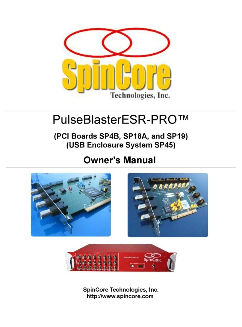
SpinCore Technologies
SpinCore Technologies PulseBlasterESR-PRO SP4B User manual
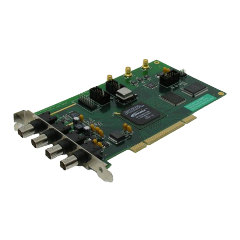
SpinCore Technologies
SpinCore Technologies RadioProcessor-G User manual
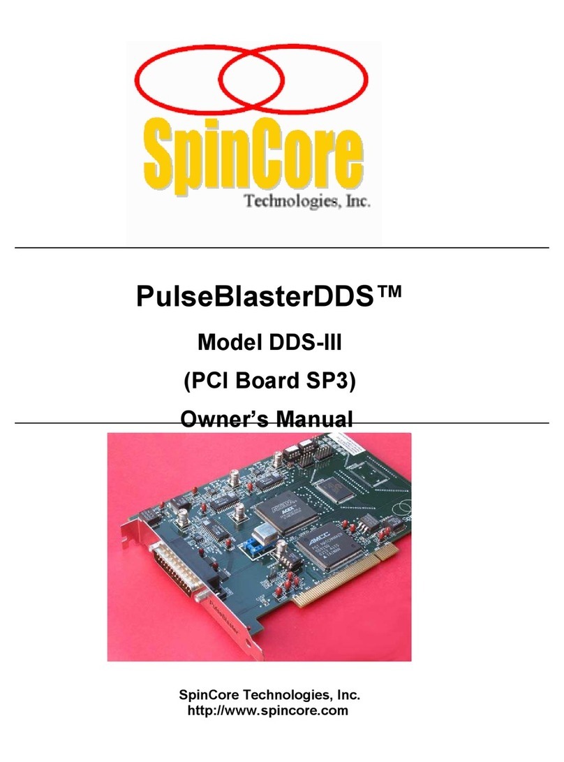
SpinCore Technologies
SpinCore Technologies PulseBlaster DDS-III User manual
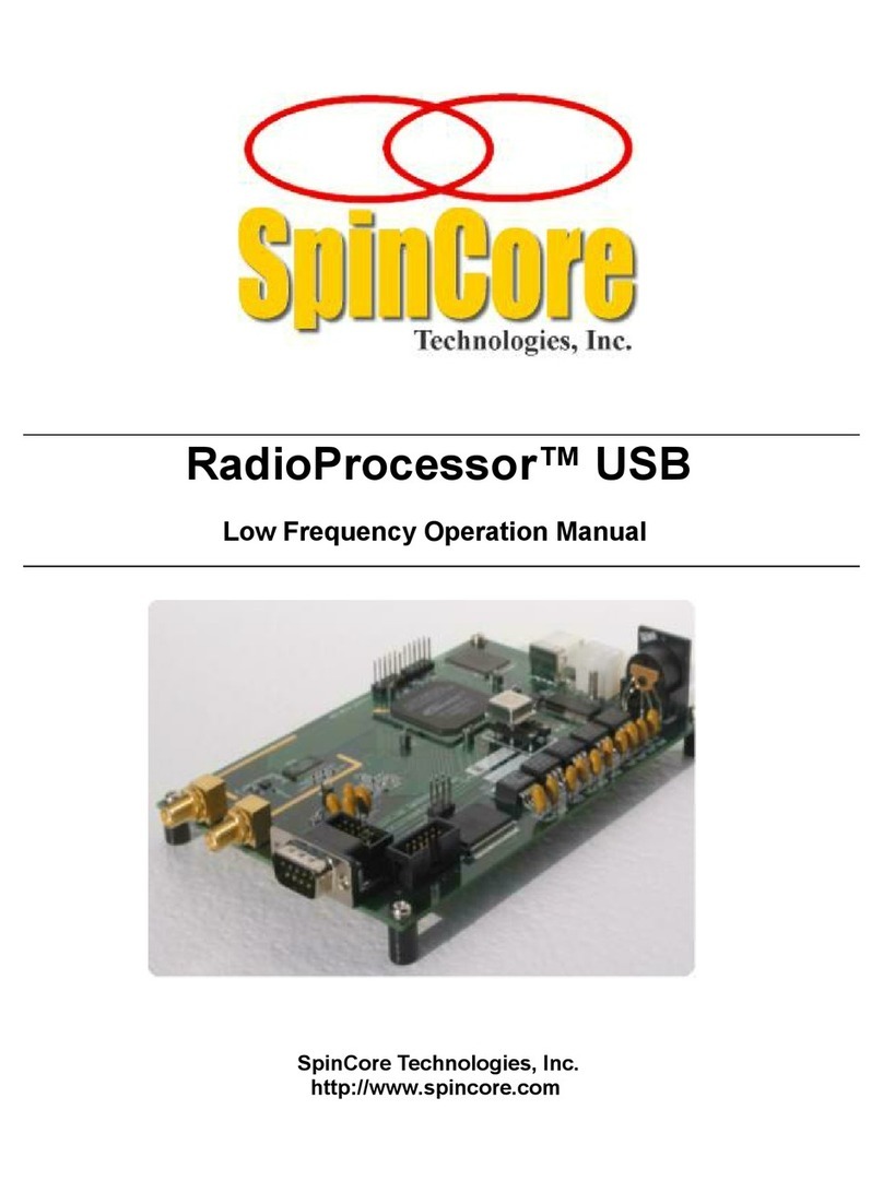
SpinCore Technologies
SpinCore Technologies RadioProcessor USB User manual
SpinCore Technologies
SpinCore Technologies PulseBlasterESR-PRO-II User manual

