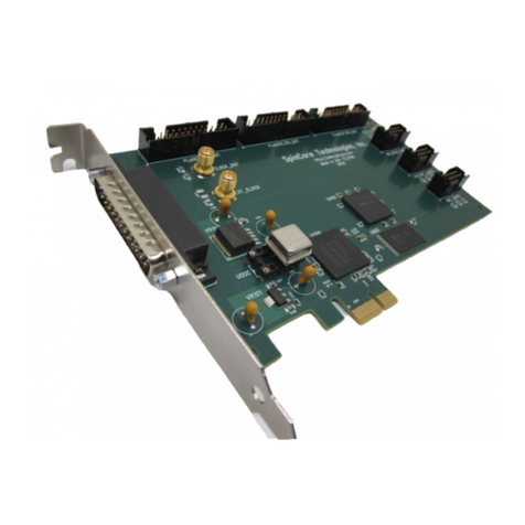
SpinCore Technologies PulseBlasterDDSII User manual

SpinCore
PulseBlasterDDSII
LabVIEW Extensions
Con ratulations and thank you for choosin a desi n from
SpinCore Technolo ies, Inc.
We appreciate your business!
At SpinCore we try to fully support the needs of our customers. If you
are in need of assistance, please contact us and we will strive to provide
the necessary support.
© 2008 SpinCore Technologies, Inc. All rights reserved.
SpinCore Technologies, Inc. reserves the right to make changes to the product(s or information herein without notice.
RadioProcessor™, PulseBlaster™, SpinCore, and the SpinCore Technologies, Inc. logos are trademarks of SpinCore Technologies, Inc.
All other trademarks are the property of their respective owners.
SpinCore Technologies, Inc. makes every effort to verify the correct operation of the equipment. This equipment version is not intended
for use in a system in which the failure of a SpinCore device will threaten the safety of equipment or person(s .
2 2011-04-29
www.spincore.com

SpinCore
PulseBlasterDDSII
LabVIEW Extensions
Table of Contents
I. Overview ....................................................................................................... 5
II. Installation ................................................................................................... 8
Method 1: Stand-Alone Executables ............................................................................ 8
Method 2: Customizable VIs ......................................................................................... 8
III. General Information ................................................................................... 9
Instruction Description .................................................................................................. 9
Re ister Descriptions .................................................................................................. 11
Path Terminals .............................................................................................................. 13
Error Terminals ............................................................................................................. 14
LabVIEW Pro ram Flow ............................................................................................... 14
IV. VI descriptions ......................................................................................... 15
Main VI ........................................................................................................................... 15
PBLV_DDSII_Interface.vi ........................................................................................ 15
Example VIs .................................................................................................................. 16
PBLV_DDSII_freq_test.vi ........................................................................................ 16
PBLV_DDSII_phase_test.vi .................................................................................... 18
PBLV_DDSII_amp_test.vi ....................................................................................... 20
Basic SubVIs ................................................................................................................. 22
pb_err r_handler.vi ................................................................................................. 22
pb_init.vi .................................................................................................................. 22
pb_set_default.vi ..................................................................................................... 22
pb_c re_cl ck.vi ...................................................................................................... 22
pb_select_dds.vi ...................................................................................................... 23
pb_start_pr gramming.vi ........................................................................................ 23
pb_set_freq.vi .......................................................................................................... 23
pb_set_phase.vi ...................................................................................................... 23
3 2011-04-29
www.spincore.com

SpinCore
PulseBlasterDDSII
LabVIEW Extensions
pb_set_amp.vi ......................................................................................................... 24
pb_inst_dds2.vi ....................................................................................................... 24
pb_st p_pr gramming.vi ......................................................................................... 24
pb_cl se.vi .............................................................................................................. 24
pb_start.vi ................................................................................................................ 25
pb_st p.vi ................................................................................................................ 25
V. Contact Information ................................................................................. 26
4 2011-04-29
www.spincore.com

SpinCore
PulseBlasterDDSII
LabVIEW Extensions
I. Overview
The SpinCore PulseBlasterDDS-II LabVIEW Extensions (PBLV-DDS-II provide the
functionality of programming and controlling digital pulse and RF generation in
PulseBlasterDDS-II boards using the simple NI LabVIEW graphical programming interface.
The package contains basic subVIs that can be used to include PulseBlasterDDS-II
interaction from your own LabVIEW programs, as well as some complete example VIs.
Additionally, all of the examples are available as stand-alone applications to control.
The PBLV-DDS-II is an intuitive graphical equivalent of the SpinAPI C functions. The GUI
(known as the front panel has all the inputs needed to access the PulseBlaster including
instruction registers, clock frequency, and buttons for loading, starting, and stopping the
board. The input is then used in the back-end code (known as the block diagram to
access the C functions that control and program the PulseBlasterDDS-II. The LabVIEW
block diagram is a one-to-one equivalent of the corresponding C code, without having to
write code. An example of the front panel and block diagram are shown in Figure 1 and
Figure 2.
Note: For information on using the the Digital Pulse Generation functionality of the board
in LabVIEW, please see the PulseBlaster LabVIEW Extensions documentation.
(http://www.spincore.com/support/PBLV/PBLV_Manual.pdf
All example VIs and subVIs are described in detail below.
5 2011-04-29
www.spincore.com

SpinCore
PulseBlasterDDSII
LabVIEW Extensions
6 2011-04-29
Figure 1: Example of PulseBlasterDDS-II LabVIEW
Extensions User Interfa e
www.spincore.com

SpinCore
PulseBlasterDDSII
LabVIEW Extensions
7 2011-04-29
Figure 2: Example of PulseBlaster-DDS-II LabVIEW Extensions Blo k Diagram
www.spincore.com

SpinCore
PulseBlasterDDSII
LabVIEW Extensions
II. Installation
There are two methods of using the PulseBlasterDDS-II LabVIEW Extensions. The first
method is a set of stand-alone executables which will control the PulseBlasterDDS-II
boards with a simple, intuitive interface with no other necessary knowledge of LabVIEW
programming. The second method is a set of LabVIEW VIs which can be used with the
LabVIEW Development platform to create custom programs using the PBLV interface.
Method 1: Stand-Alone Executables
In order for PBLV-DDS-II stand-alone executables to work, the following must be installed:
●SpinCore Driver Suite - Please see the SpinCore Driver Suite Installation Guide
(http://www.spincore.com/support/spinapi/instructions/ for more information.
●National Instruments LabVIEW Run-Time Engine 2010
(http://www.spincore.com/support/PBLV/LVRTE2010std.exe - Note if you have
LabVIEW 2010 or later installed, this is not needed.
●LabVIEW PulseBlaster Extensions Stand-Alone executables located here.
Method 2: Customizable VIs
In order for PBLV-DDS-II customizable VIs to work, the following must be installed:
●SpinCore Driver Suite - Please see the SpinCore Driver Suite Installation Guide
(http://www.spincore.com/support/spinapi/instructions/ for more information.
●National Instruments LabVIEW 8.6 or later - If you do not have LabVIEW 8.6 or later
installed, you may download a 30-day evaluation
(https://lumen.ni.com/nicif/us/lveval/content.xhtml of the latest LabVIEW
development software.
(NOTE: Customizable VIs for versions of LabVIEW as old as LabVIEW 8.0 are
available. For customizable VIs older than LabVIEW 8.6 please contact SpinCore
Technologies via the web forum.
●LabVIEW PulseBlaster Extensions located here.
(NOTE: Customizable VIs use the C-calling convention. For customizable VIs that
use the WINAPI calling convention please contact SpinCore Technologies via the
web forum.
8 2011-04-29
www.spincore.com

SpinCore
PulseBlasterDDSII
LabVIEW Extensions
III. General Information
Instruction Description
Throughout the PulseBlasterDDS-II LabVIEW Extension,
the instruction word, corresponding to a given interval in
the pulse sequence, is given as shown to the left. The
instruction on the front panel (Figure 3 is broken up into
15 fields displayed from top to bottom:
●Comment space is an empty text box. This area is
used to annotate your instruction and is not
programmed onto the PulseBlasterDDS-II board.
●Time is the duration that the current instruction is to
be held in microseconds. Range and resolution
varies depending on what board is being used. This
corresponds to “length” in SpinAPI.
●Output Pattern determines the state of each TTL
output bit. If an LED is on then it's corresponding
output bit is high, and if the LED is off then it's
corresponding output bit is low. This corresponds to
“flags” in SpinAPI.
●DDS0 RF Output Enable tells the DDS-II board
whether the RF output for DDS0 should be enabled
during this instruction. This corresponds to “dds_en0”
in SpinAPI.
●DDS0 Phase Reset tells the DDS-II board to reset
the phase of all DDS0 channels to their time=0
phase. They will stay in this state until the value of
this bit returns to 0. This corresponds to
“phase_reset0” in SpinAPI.
●DDS0 Frequency Register Selects determines which
frequency register will be used for the RF output of
DDS0 during this instruction. Refer to your board
manual for the number of frequency registers
available. This corresponds to “freq0” in SpinAPI.
●DDS0 Phase Register Selects determines which
phase register will be used for the RF output of DDS0
9 2011-04-29
Figure 3: PulseBlaster
Instru tion
www.spincore.com

SpinCore
PulseBlasterDDSII
LabVIEW Extensions
during this instruction. Refer to your board manual for the number of phase registers
available. This corresponds to “phase0” in SpinAPI.
●DDS0 Amplitude Register Selects determines which amplitude register will be used
for the RF output of DDS0 during this instruction. Refer to your board manual for the
number of amplitude registers available. This corresponds to “amp0” in SpinAPI.
●DDS1 RF Output Enable tells the DDS-II board whether the RF output for DDS1
should be enabled during this instruction. This corresponds to “dds_en1” in SpinAPI.
●DDS1 Phase Reset tells the DDS-II board to reset the phase of all DDS1 channels to
their time=0 phase. They will stay in this state until the value of this bit returns to 0.
This corresponds to “phase_reset1” in SpinAPI.
●DDS1 Frequency Register Selects determines which frequency register will be used
for the RF output of DDS1 during this instruction. Refer to your board manual for the
number of frequency registers available. This corresponds to “freq1” in SpinAPI.
●DDS1 Phase Register Selects determines which phase register will be used for the
RF output of DDS1 during this instruction. Refer to your board manual for the
number of phase registers available. This corresponds to “phase1” in SpinAPI.
●DDS1 Amplitude Register Selects determines which amplitude register will be used
for the RF output of DDS1 during this instruction. Refer to your board manual for the
number of amplitude registers available. This corresponds to “amp1” in SpinAPI.
●Program Flow determines the flow of program instructions after the bit pattern is
displayed. This corresponds to “inst” in SpinAPI. Available instructions are:
○CONTINUE - Program execution continues to next instruction.
○STOP - Stop execution of program.
○LOOP - Specify beginning of a loop. Execution continues to next instruction.
Instruction data used to specify number of loops.
○END_LOOP Execution returns to beginning of loop and decrements loop
counter. Instruction data used to specify beginning of loop.
○JSR - Program execution jumps to beginning of a subroutine. Instruction data
used to specify address of first subroutine instruction.
○RTS - Program execution returns to instruction after JSR was called.
○BRANCH - Program execution continues at specified instruction. Instruction
data specifies address of next instruction.
○LONG_DELAY - For long interval instructions. Data field specifies a multiplier
of the length field. Execution continues to next instruction.
○WAIT - Program execution stops and waits for software or hardware trigger.
Execution continues to next instruction after receipt of trigger. (Please see
SpinAPI documentation for more information on limits of certain Op Codes
●Instruction Data is the data to be used for certain instructions determined by the Op
Code. This corresponds to “inst_data” in SpinAPI. Note for certain instructions this
field is not used.
10 2011-04-29
www.spincore.com

SpinCore
PulseBlasterDDSII
LabVIEW Extensions
Figure 4 Below shows detail of the corresponding instruction word as depicted in
LabVIEW's block diagram.
Register Descriptions
In each PBLV-DDS-II program there are 6 banks of registers, 3 banks of registers for
each DDS core, which must be set before programming the board. There are frequency
registers, phase registers and amplitude registers for each DDS core as shown in Figure 5.
Frequencies are specified in MHz and can be programmed in the range specified in
your board manual. The registers shown on the front panel range from 0 at the top down
to 15 at the bottom, but the number of frequency registers available vary depending on the
board. See your board manual for the number of output frequency registers available. The
specific frequency registers must be set in the register bank in order to be used in an
instruction as described above. If the register box is white, then it will be programmed to
the board and can be used. If it is grayed out, it will not be programmed and therefore
cannot be used in an instruction. To make a grayed out register box white, simply click
inside the box and type the value you want. To gray out a white register box, right-click on
the box, select “Data Operations”, and then select “Delete Element.” The register chosen
by the “DDS0 Frequency Register Selects” instruction from Figure 3 corresponds to the
frequency registers under the heading, “DDS0 Registers” in Figure 5. Similarly the “DDS1
Frequency Register Selects” instruction corresponds to the frequency registers under the
heading, “DDS1 Registers”.
11 2011-04-29
Figure 4: Example of how the instru tion is reated and sent to the board in
the PBLV-DDS-II Blo k Diagram
www.spincore.com

SpinCore
PulseBlasterDDSII
LabVIEW Extensions
Phases are specified in degrees and can be set from 0.0 to 365.0 degrees. The
registers shown on the front panel range from 0 at the top down to 15 at the bottom, but
the number of phase registers available vary depending on the board. See your board
manual for the number of output phase registers available. The specific phase registers
must be set in the register bank in order to be used in an instruction as described above. If
the register box is white, then it will be programmed to the board and can be used. If it is
grayed out, it will not be programmed and therefore cannot be used in an instruction. To
make a grayed out register box white, simply click inside the box and type the value you
want. To gray out a white register box, right-click on the box, select “Data Operations”, and
then select “Delete Element.” The register chosen by the “DDS0 Phase Register Selects”
instruction from Figure 3 corresponds to the phase registers under the heading, “DDS0
Registers” in Figure 5. Similarly the “DDS1 Phase Register Selects” instruction
corresponds to the phase registers under the heading, “DDS1 Registers”.
Amplitudes are specified as a percentage of full power and ranges from 0.0 to 1.0.
The registers shown on the front panel range from 0 at the top down to 3 at the bottom.
There are only 4 amplitude registers available. The specific frequency registers must be
set in the register bank in order to be used in an instruction as described above. If the
register box is white, then it will be programmed to the board and can be used. If it is
grayed out, it will not be programmed and therefore cannot be used in an instruction. To
make a grayed out register box white, simply click inside the box and type the value you
want. To gray out a white register box, right-click on the box, select “Data Operations”, and
then select “Delete Element.” The register chosen by the “DDS0 Amplitude Register
Selects” instruction from Figure 3 corresponds to the amplitude registers under the
heading, “DDS0 Registers” in Figure 5. Similarly the “DDS1 Amplitude Register Selects”
instruction corresponds to the amplitude registers under the heading, “DDS1 Registers”.
12 2011-04-29
www.spincore.com

SpinCore
PulseBlasterDDSII
LabVIEW Extensions
Path Terminals
All of the SubVIs have path input and output terminals. This is a reference to the
path where spinapi.dll is installed on the PC. The default is
C:\SpinCore\SpinAPI\dll\spinapi.dll however this may be changed depending on the
installation. All subVIs should have the “path in” connected. For ease of programming, the
path terminals can be daisy chained since all subVIs point to the same dll. See Figure 6
and Figure 7 for an example of chaining these terminals.
13 2011-04-29
Figure 7: Example of haining path and error
terminals
Figure 6: Path and error terminals
www.spincore.com
Figure 5: Frequen y, Phase and Amplitude
Registers for both DDS ores

SpinCore
PulseBlasterDDSII
LabVIEW Extensions
Error Terminals
All of the SubVIs have error input and output terminals. When a VI is built, the “error
out” terminal of a subVI should be connected to the “error in” terminal of the following
subVI. These terminals are used to help facilitate sequential execution of the functions, as
well as provide debugging information to the user if an error occurs in the VI. See Figure 6
and Figure 7 for an example of these terminals. When chaining, the order of the subVIs
corresponds to the order in which the functions will be called.
LabVIEW Program Flow
The LabVIEW Block diagram is set up to independently control the four major
functions (start/restart, stop/reset, load, change using four while loops running in parallel.
Within each loop is another loop that continuously waits for the specified button to be
pressed. Once the button is pressed, the inner loop will exit and program flow will be
passed to the chain of subVIs. After the chain of functions complete, program flow will
return to the inner loop to wait for the button again. An example of this is shown in Figure
8.
14 2011-04-29
Figure 8: LabVIEW Program Flow Example
www.spincore.com

SpinCore
PulseBlasterDDSII
LabVIEW Extensions
IV. VI descriptions
Main VI
PBLV_DDSII_Interface. i
The PBLV-DDSII Interface VI allows the user complete control of the
PulseBlasterDDS board.
To start the VI press the Run button at the top of the LabVIEW window (for stand-
alone programs, the program is run automatically when opened . First you must insert the
clock frequency value of the board into the “clock_freq (MHz ” field as well as the path to
spinapi.dll as described above. Next, make any instruction set you want by editing the
instruction fields. Use the “# of Instructions” field to increase or decrease the number of
instructions you want to program. Once you have your instruction set, you can edit the
frequency, phase, and amplitude registers for each DDS core to the values you want.
When the instructions and registers are set up correctly, you must first load the
board by clicking the “LOAD BOARD” button and then wait until the button becomes
inactive. To start the program click on the “START” button, and to stop the program click
on the “STOP” button. If there are multiple boards connected to your computer, the
“CHANGE BOARD” button will change the board that is being programmed to the one
specified by the “board_num” field. All four functions are independent and may be run at
any time, however an instruction sequence must be loaded into the board before it can be
started. Caution: After pressing STOP, all digital output bits may maintain their final state.
The RF output will return to 0V when the stop button is pressed.
See Figure 1 for a screen shot of the PBLV-DDSII Interface.
15 2011-04-29
www.spincore.com

SpinCore
PulseBlasterDDSII
LabVIEW Extensions
Example VIs
PBLV_DDSII_freq_test. i
This PBLV-DDS-II Frequency Example VI outputs a sine wave with DDS0, cycling
through 4 different frequencies which are set in the frequency registers. It also outputs a
sine wave with DDS1, cycling through the same 4 frequencies but in reverse order.
To start the VI press the Run button at the top of the LabVIEW window (for stand-
alone programs, the program is run automatically when opened . First you must insert the
clock frequency value of the board into the “clock_freq (MHz ” field as well as the path to
spinapi.dll as described above. Next, the appropriate frequency, phase, and amplitude
registers must be set. Both DDS cores initially have these values for their registers:
frequency registers 0, 1, 2, and 3 are set to 1, 5, 10 and 15 MHz respectively, phase
register 0 is set to 0 degrees, and amplitude register 0 is set to 1. Then the instructions
must be set up appropriately. This VI programs the PBDDS-II board with 6 instructions.
The first instruction resets the phase and the RF output is disabled for both DDS cores.
The next four instructions enable output for 2 μs and frequency register 0, 1, 2, and 3
respectively for DDS0 and frequency register 3, 2, 1, and 0 respectively for DDS1. All
instructions use phase register 0 and amplitude register 0. The last instruction disables the
output for 1 ms to allow for oscilloscope triggering. You may change these instructions,
and registers as desired.
When the instructions and registers are set up correctly, you must first load the
board by clicking the “LOAD BOARD” button and then wait until the button becomes
inactive. To start the program click on the “START” button, and to stop the program click
on the “STOP” button. If there are multiple boards connected to your computer, the
“CHANGE BOARD” button will change the board that is being programmed to the one
specified by the “board_num” field. All four functions are independent and may be run at
any time, however an instruction sequence must be loaded into the board before it can be
started. Caution: After pressing STOP, all digital output bits may maintain their final state.
The RF output will return to 0V when the stop button is pressed.
See Figure 9 for a screen shot of the PBLV-DDSII Frequency Test.
16 2011-04-29
www.spincore.com

SpinCore
PulseBlasterDDSII
LabVIEW Extensions
17 2011-04-29
www.spincore.com

SpinCore
PulseBlasterDDSII
LabVIEW Extensions
18 2011-04-29
Figure 9: LabVIEW PulseBlasterDDSII Extension – Frequen y
Test
www.spincore.com

SpinCore
PulseBlasterDDSII
LabVIEW Extensions
PBLV_DDSII_phase_test. i
This PBLV-DDS-II Phase Example VI outputs a sine wave with DDS0, cycling
through 4 different phases which are set in the phase registers. It also outputs a sine wave
with DDS1, cycling through the same 4 phases but in reverse order.
To start the VI press the Run button at the top of the LabVIEW window (for stand-
alone programs, the program is run automatically when opened . First you must insert the
clock frequency value of the board into the “clock_freq (MHz ” field as well as the path to
spinapi.dll as described above. Next, the appropriate frequency, phase, and amplitude
registers must be set. Both DDS cores initially have these values for their registers: phase
registers 0, 1, 2, and 3 are set to 0°, 90°, 180°, and 270° respectively, frequency register 0
is set to 1 MHz, and amplitude register 0 is set to 1. Then the instructions must be set up
appropriately. This VI programs the PBDDS-II board with 6 instructions. The first
instruction resets the phase and the RF output is disabled for both DDS cores. The next
four instructions enable output for 2 μs and use phase register 0, 1, 2, and 3 respectively
for DDS0, and phase register 3, 2, 1, and 0 respectively for DDS1. All instructions use
frequency register 0 and amplitude register 0. The last instruction disables the output for 1
ms to allow for oscilloscope triggering. You may change these instructions, and registers
as desired.
When the instructions and registers are set up correctly, you must first load the
board by clicking the “LOAD BOARD” button and then wait until the button becomes
inactive. To start the program click on the “START” button, and to stop the program click
on the “STOP” button. If there are multiple boards connected to your computer, the
“CHANGE BOARD” button will change the board that is being programmed to the one
specified by the “board_num” field. All four functions are independent and may be run at
any time, however an instruction sequence must be loaded into the board before it can be
started. Caution: After pressing STOP, all digital output bits may maintain their final state.
The RF output will return to 0V when the stop button is pressed.
See Figure 10 for a screen shot of the PBLV-DDSII Phase Test.
19 2011-04-29
www.spincore.com

SpinCore
PulseBlasterDDSII
LabVIEW Extensions
20 2011-04-29
www.spincore.com
This manual suits for next models
1
Table of contents
Other SpinCore Technologies Pulse Generator manuals

