Struck SIS3153 User manual

SIS Documentation
SIS3153
VME interface
Page 1 of 38
SIS3153
USB3/Ethernet VME Interface
User Manual
SIS GmbH
Harksheider Str. 102A
22399 Hamburg
Germany
Phone:
++49 (0) 40 60 87 305 0
Fax:
++49 (0) 40 60 87 305 20
http://www.struck.de
Version: sis3153-M-usb-1-V105-manual.doc as of 08.09.2015
Struck Documentation
SIS3153
VME interface
Page 2 of 38
Revision Table:
Revision
Date
Modification
1.00
25.10.2013
First official release
1.01
29.10.2013
Minor touch up
1.02
26.11.2014
Hardware version 2
-FX3 boot mode added
1.03
01.12.2014
Software section, minor touch up
1.04
21.01.2015
USB cable length appendix
1.05
08.09.2015
Description of Switch 162-3: Link Led L (USB or Ethernet)

SIS Documentation
SIS3153
VME interface
Page 3 of 38
1 Table of contents
1Table of contents .................................................................................................................3
1Introduction ......................................................................................................................... 4
2Functionality........................................................................................................................5
3USB device..........................................................................................................................6
3.1 SIS3153 USB Register space .................................................................................................................. 6
3.1.1 USB Register Space Address Map.................................................................................................. 7
3.2 USB Register description........................................................................................................................ 8
3.2.1 USB Control/Status Register(write/read)........................................................................................ 8
3.2.2 Module Id. and Firmware Revision Register ( read)..................................................................... 10
3.2.3 Serial Number register .................................................................................................................. 11
3.2.4 LEMO IO control register............................................................................................................. 12
3.2.5 UDP protocol configuration register ............................................................................................. 13
3.2.6 USB VME Master Status/Control register (read/write) ................................................................ 14
3.2.7 USB VME Master Cycle Status.................................................................................................... 16
3.2.8 USB VME Interrupt Status Register ............................................................................................. 17
3.3 VME Bus............................................................................................................................................... 18
4USB –SIS3153 Transfer Data Rate..................................................................................19
4.1 USB –SIS3153 Internal Space Data Rate............................................................................................. 19
4.2 USB –SIS3153 VME Space Data Rate ................................................................................................ 20
4.2.1 VME Data Rate measured with a Chrislin VME Memory............................................................ 20
4.2.2 VME Data Rate measured with a SIS3305 ADC.......................................................................... 21
5Front Panel Elements.........................................................................................................22
6LEDs..................................................................................................................................23
6.1 Front Panel LEDs.................................................................................................................................. 23
6.2 SMD LEDs............................................................................................................................................ 25
7SIS3153 Jumpers, Switches and Connectors.....................................................................26
7.1 CON100 JTAG ..................................................................................................................................... 26
7.2 SW161/SW160 VME Slave Address (future feature)........................................................................... 27
7.3 SW162 Dip switch System Controller/Reset Behavior/Slave Addressing............................................ 27
7.4 JP123 LEMO input, JP133 LEMO output logic level........................................................................... 28
J126 USB Controller FX3 UART interface ...................................................................................................... 29
7.5 FX3 Boot mode (SIS3153 V2 / SN006 and above)............................................................................... 30
8VME master/system controller..........................................................................................31
8.1 Multi master operation .......................................................................................................................... 31
8.1.1 System Controller.......................................................................................................................... 31
8.1.2 Bus grant/bus mastership .............................................................................................................. 31
9Connector types.................................................................................................................32
10 Software .........................................................................................................................32
10.1 Windows ............................................................................................................................................... 32
10.1.1 Ethernet......................................................................................................................................... 32
10.1.2 USB............................................................................................................................................... 32
10.2 LINUX .................................................................................................................................................. 33
10.2.1 Ethernet......................................................................................................................................... 33
10.2.2 USB............................................................................................................................................... 33
11 Appendix........................................................................................................................34
11.1 Power Consumption.............................................................................................................................. 34
11.2 USB3.0 cable length.............................................................................................................................. 35
12 Index...............................................................................................................................37
Struck Documentation
SIS3153
VME interface
Page 4 of 38
1 Introduction
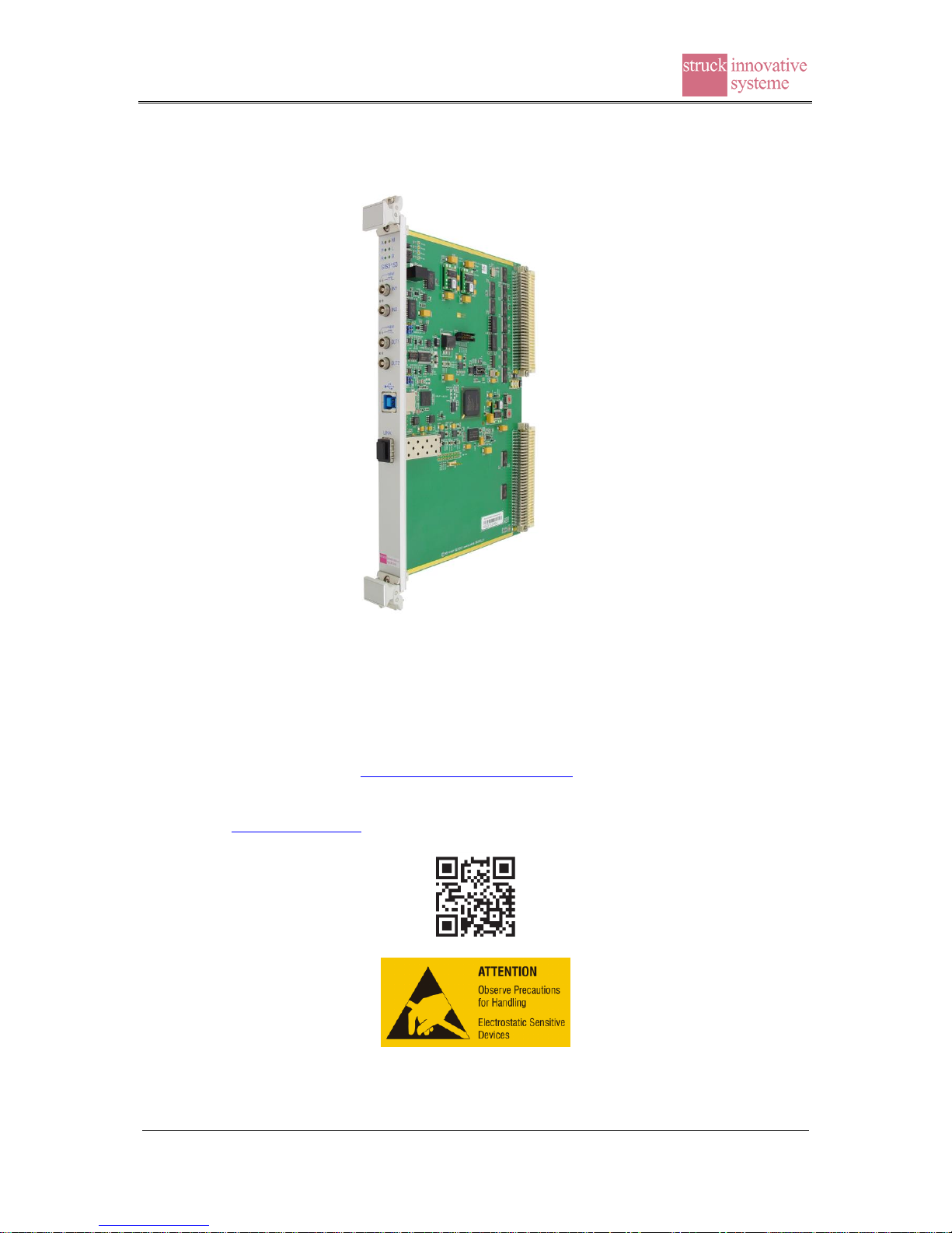
The SIS3153 USB3.0/Ethernet to VME interface is a single width 6U VME card.
Photograph of SIS3153
As we are aware, that no manual is perfect, we appreciate your feedback and will incorporate proposed
changes and corrections as quickly as possible. The most recent version of this manual can be obtained
by email from info@struck.de.
Feel free to apply for an account for our Dokuwiki documentation web page also.
The SIS3153 firmware page is at www.struck.de/sis3153firm.html .
Information on SIS3153 applications, firmware news and other related issues will be posted on our
DAQ blog at www.struck.de/blog also.

SIS Documentation
SIS3153
VME interface
Page 5 of 38
2 Functionality
The SIS3153 interfaces the popular Universal Serial Bus (USB) and Ethernet to the VMEbus.
It uses the Cypress Semiconductor Corporation FX3 chip as USB3.0 host controller. The
modules functionality comprises:
Ethernet (UDP) connectivity (Described in ‘SIS3153 - Ethernet Addendum’)
USB3.0 / Superspeed USB functionality
USB2.0 and USB1.1 compliance
VME master read cycles:
-IACK, A16/A24/A32
-D8/D16/D32/BLT32/MBLT64/2eVME/2eSST160/2eSST267/2eSST320
VME master write cycles:
-A16/A24/A32
-D8/D16/D32/BLT32/MBLT64/2eVME
VME slave; not implemented yet
2 digital front panel inputs (NIM or TTL level, select by jumper or register bits)
2 digital front panel outputs (NIM or TTL level , select by jumper or register bits)
Possible future firmware extensions comprise
Optical connectivity
Note: A Gigabit 1000BASE-T copper SFP transceiver (Finisar FCLF-8520-3 or compatible,
Struck part number 04333) is required for Ethernet operation. The transceiver is included with
the SIS3153 if the card is ordered for Ethernet to VME Interface operation (Struck part
number 05867).

Struck Documentation
SIS3153
VME interface
Page 6 of 38
3 USB device
The SIS3153USB device (USB peripheral) is hotplugging.
The SIS3153USB device in combination with the drivers supports access to following spaces.
-SIS3153 USB register space
-VME Bus
3.1 SIS3153 USB Register space
The driver offers the following calls:
int sis3153Usb_Register_Single_Read(HANDLE usbDevice,
ULONG addr, ULONG* data) ;
int sis3153Usb_Register_Dma_Read(HANDLE usbDevice,
ULONG addr, ULONG* dmabufs,
ULONG req_nof_data, ULONG* got_nof_data) ;
int sis3153Usb_Register_Single_Write(HANDLE usbDevice,
ULONG addr, ULONG data) ;
int sis3153Usb_Register_Dma_Write(HANDLE usbDevice,
ULONG addr, ULONG* dmabufs,
ULONG req_nof_data, ULONG* put_nof_data);
SIS Documentation
SIS3153
VME interface
Page 7 of 38
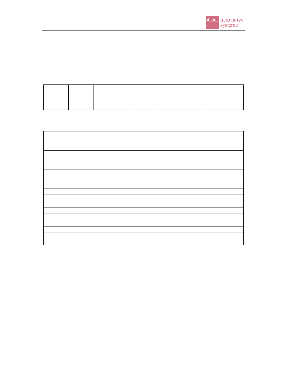
3.1.1 USB Register Space Address Map
Offset
R/W
Function/Register
0x0
R/W
USB Control/Status register
0x1
R
Module Id. and firmware version register
0x2
R
Serial Number register
0x3
R/W
LEMO IO control register
0x4
R/W
UDP protocol configuration register
0x10
R/W
USB VME Master Status/Control register
0x11
R
USB VME Master Cycle Status Register
0x12
R
USB VME Interrupt Status Register
0x100
KA
Key reset all
0x 0000 1000
R/W
Internal RAM
..
0x 0000 1FFF
0x 0010 0000
R
USB Address/Data Test space:
Read Data = Read Address
..
0x 001F FFFF
0x 0020 0000
R
USB Speed Test space:
Read Data = Speed Counter
The Speed Counter increments every 8ns (125 MHz)
..
0x 002F FFFF
The shorthand KA stands for key address. Write access with arbitrary data to a key address
initiates the specified function
Struck Documentation
SIS3153
VME interface
Page 8 of 38
3.2 USB Register description
The function of the individual registers is described in detail in this section.
The first line after the subsection header (in Courier font) like:
#define SIS3153_CONTROL_STATUS 0x0
refers to the sis3153usb.h header file.
3.2.1 USB Control/Status Register(write/read)
#define SIS3153USB_CONTROL_STATUS 0x0
The control register is in charge of the control of some basic properties of the SIS3153 board,
like enabling Led test mode. It is implemented via a selective J/K register, a specific function
is enabled by writing a 1 into the set/enable bit, the function is disabled by writing a 1 into the
clear/disable bit (which location is 16-bit higher in the register). An undefined toggle status
will result from setting both the enable and disable bits for a specific function at the same
time.
On read access the same register represents the status register.
Bit
write Function
read Function
31
reserved
0
30
reserved
0
29
reserved
USB speed flag bit 1
28
reserved
USB speed flag bit 0
27
reserved
0
26
reserved
0
25
reserved
0
24
reserved
0
23
reserved
0
22
reserved
0
21
reserved
0
20
Clear SPI-Flash interface reset (*)
0
19
Clear USB internal access control bit 1 (*)
0
18
Clear USB internal access control bit 0 (*)
0
17
Clear Led test mode (*)
0
16
Switch off LED A (*)
0
15
reserved
Status reserved
..
..
..
6
..
..
5
reserved
Status reserved
4
Set SPI-Flash interface reset
Status SPI-Flash interface reset
3
Set USB internal access control bit 1
Status USB internal access control bit 1
2
Set USB internal access control bit 0
Status USB internal access control bit 0
1
Set Led test mode
Status Led test mode
0
Switch on LED A
Status User LED A
(1=LED on, 0=LED off)
(*) denotes power up default setting, i.e. the power up reading of the register is 0x0
USB internal access control bits:
SIS Documentation
SIS3153
VME interface
Page 9 of 38
Bit 1
Bit 0
Internal read speed to USB3 controller
0
0
16 ns / 32-bit word
0
1
8 ns / 32-bit word
1
0
1 us / 32-bit word
1
1
reserved
This feature is used for test purposes only.
Struck Documentation
SIS3153
VME interface
Page 10 of 38
3.2.2 Module Id. and Firmware Revision Register ( read)
#define SIS3153USB_MODID_VERSION 0x1
This register reflects the module identification of the SIS3153USB and its minor and major
firmware revision levels. The major revision level will be used to distinguish between
substantial design differences and experiment specific designs, while the minor revision level
will be used to mark user specific adaptations.
Bit
Function
Reading
31
Module Id. Bit 15
3
30
Module Id. Bit 14
29
Module Id. Bit 13
28
Module Id. Bit 12
27
Module Id. Bit 11
1
26
Module Id. Bit 10
25
Module Id. Bit 9
24
Module Id. Bit 8
23
Module Id. Bit 7
5
22
Module Id. Bit 6
21
Module Id. Bit 5
20
Module Id. Bit 4
19
Module Id. Bit 3
3
18
Module Id. Bit 2
17
Module Id. Bit 1
16
Module Id. Bit 0
15
Major Revision Bit 7
14
Major Revision Bit 6
13
Major Revision Bit 5
12
Major Revision Bit 4
11
Major Revision Bit 3
10
Major Revision Bit 2
9
Major Revision Bit 1
8
Major Revision Bit 0
7
Minor Revision Bit 7
6
Minor Revision Bit 6
5
Minor Revision Bit 5
4
Minor Revision Bit 4
3
Minor Revision Bit 3
2
Minor Revision Bit 2
1
Minor Revision Bit 1
0
Minor Revision Bit 0
Major revision number
Application/user
0x01
Generic SIS3153USB design (internal 32-bit interface support)
0x16
Generic SIS3153USB design (internal 16-bit interface support)
SIS Documentation
SIS3153
VME interface
Page 11 of 38
3.2.3 Serial Number register
#define SIS3153USB_SERIAL_NUMBER_REG 0x2
This register holds the Serial Number of the module.
BIT
access
Name
Function
31-17
FFFE0000
RO
reserved
16
00010000
RO
Serial Number Not Valid Flag
0: valid
1: not valid
15-0
0000FFFF
RO
Serial Number
1..65535
Note: The Ethernet MAC address is 00-00-56-15-3n-nn (n-nn is the Serial Number)
Struck Documentation
SIS3153
VME interface
Page 12 of 38
3.2.4 LEMO IO control register
#define SIS3153USB_LEMO_IO_CTRL_REG 0x3
The register is implemented in a J/K fashion also and allows to check the status of the logic
level setting of the front panel inputs and outputs. In addition it can be used to control the
levels by software. Please note, that the actual control over the status of the inputs and outputs
is controlled via the LEMO I/O register
Bit
Write Function
Read Function/value
31
Disable Software Level Control (*)
0
30
reserved
0
29
reserved
0
28
reserved
0
27
reserved
0
26
reserved
0
25
reserved
0
24
reserved
0
23
Clear output 2 latch (*)
Status of input 2 latch
22
Clear output 1 latch (*)
Status of input 1 latch
21
Clear output 2 (*)
Status of input 2
20
Clear output 1 (*)
Status of input 1
19
Set input 2 to NIM level (*)
0
18
Set input 1 to NIM level (*)
0
17
Set output 2 to NIM level (*)
0
16
Set output 1 to NIM level (*)
0
15
Enable Software Level Control
Status Software Level Control
14
reserved
Status of reserved
13
reserved
Status of reserved
12
reserved
Status of reserved
11
reserved
Status of reserved
10
reserved
Status of reserved
9
reserved
Status of reserved
8
reserved
Status of reserved
7
Generate output pulse 2
0
6
Generate output pulse 1
0
5
Set output 2
Status of output 2
4
Set output 1
Status of output 1
3
Set input 2 to TTL level
Status of level input 2 (0=NIM, 1=TTL)
2
Set input 1 to TTL level
Status of level input 1 (0=NIM, 1=TTL)
1
Set output 2 to TTL level
Status of level output 2 (0=NIM, 1=TTL)
0
Set output 1 to TTL level
Status of level output 1 (0=NIM, 1=TTL)
The power up value is 0x00000000 (with the I/Os jumper configured to NIM level)
(*) denotes the power up default setting
Note 1: Enable software control by setting bit 15 to gain software control over the logic levels
of the I/Os. By default the level is defined by jumpers JP123 and JP133.
Note 2: for the typical application it will be good enough to set the logic levels to the desired
levels in hardware by setting JP123 and JP133 accordingly.
SIS Documentation
SIS3153
VME interface
Page 13 of 38
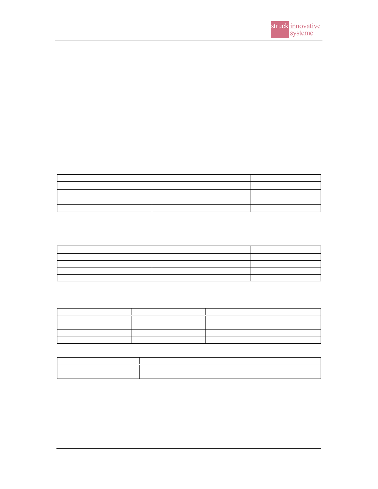
3.2.5 UDP protocol configuration register
#define SIS3153_UDP_PROTOCOL_CONFIG 0x4 /* read/write; D32 */
This register is used to control the UDP data packets. The setup of the ethernet interface is
described in detail in ‘SIS3153USB - Ethernet UDP Addendum’.
Bit
31 - 9
8
7 - 5
4
3 - 0
Function
reserved
UDP transmit
Data packet
format bit
reserved
UDP transmit jumbo
Packet enable bit
UDP transmit
packet gap bits
UDP transmit
packet gap value
Gap time between UDP packets
0
256 ns
1
512 ns
2
1 us
3
2 us
4
4 us
5
8 us
6
10 us
7
12 us
8
14 us
9
16 us
0xA
20 us
0xB
28 us
0xC
32 us
0xD
41 us
0xE
50 us
0xF
57 us
The power up default value reads 0x 00000000

Struck Documentation
SIS3153
VME interface
Page 14 of 38
3.2.6 USB VME Master Status/Control register (read/write)
#define SIS3153USB_VME_MASTER_CONTROL_STATUS 0x10
The control register is in charge of the control of most of the basic properties of the SIS3153
board in write access. It is implemented via a selective J/K register, a specific function is
enabled by writing a 1 into the set/enable bit, the function is disabled by writing a 1 into the
clear/disable bit (which location is 16-bit higher in the register). An undefined toggle status
will result from setting both the enable and disable bits for a specific function at the same
time.
Bit
Write Function
Read Function
31
Clear SYSTEM VME BERR TIMER BIT1
0
30
Clear SYSTEM VME BERR TIMER BIT0
0
29
Clear LONG TIMER BIT1
0
28
Clear LONG TIMER BIT0
0
27
no function
0
26
Clear Force Dearbit
0
25
no function
0
24
Disable VME retry
0
23
no function
0
22
Clear VME REQUESTER TYPE BIT
0
21
Clear VME_REQ_LEVEL BIT1
0
20
Clear VME_REQ_LEVEL BIT0
0
19
no function
0
18
no function
0
17
Clear VME_SYSRESET bit
0
16
Clear VME System Controller Enable bit
Status VME System Controller (*2)
15
Set SYSTEM VME BERR TIMER BIT1
Status SYSTEM VME BERR TIMER BIT1
14
Set SYSTEM VME BERR TIMER BIT0
Status SYSTEM VME BERR TIMER BIT0
13
Set LONG TIMER BIT1
Status LONG TIMER BIT1
12
Set LONG TIMER BIT0
Status LONG TIMER BIT0
11
no function
0
10
Set Force Dearbit (*5)
Status Force Dearbit Enable bit
9
no function
0
8
Enable VME retry (*4)
Status VME retry Enable bit
7
no function
0
6
Set VME REQUESTER TYPE BIT
Status VME REQUESTER TYPE BIT
5
Set VME_REQ_LEVEL BIT1
Status VME_REQ_LEVEL BIT1
4
Set VME_REQ_LEVEL BIT0
Status VME_REQ_LEVEL BIT0
3
no function
0
2
no function
0
1
Set VME_SYSRESET bit (*3)
Status VME_SYSRESET bit
0
Set VME System Controller Enable bit (*1)
Status VME System Controller Enable bit
The power up value is 0x0000C100 (or 0x0001C100 with system controller set)
Notes:
(*1) is ored with switch 5 of SW162; Caution: if the jumper is not installed and the VME
system controller functionality is enabled by software, the 16 MHz clock is not active
during power up. This may result in problems with peculiar VME slave designs that use
the VME clock to initialise on board logic.
(*2) is set with switch 5 of SW162 on or if VME System Controller Enable bit is set
SIS Documentation
SIS3153
VME interface
Page 15 of 38
(*3) if Switch SW162-7 is ON and VME_SYSRESET bit is set then VME_SYSRESET is
issued
(*4) A retry error (error code 0x212) may be caused by older VME backplanes, which do not
properly terminate this previously reserved (pin B3 on connector P2) if retry is enabled.
Retry can be disabled by setting bit 24. Retry had to be activated by setting bit 8 on the
SIS3153, this behaviour is not compatible with SST transfers.
(*5) Setting bit 10 causes the SIS3153 to release busy for 170 ns in between of blockletts
during a block transfer. This gives another master the possibility to gain busmastership
during the block transfer. The SIS3153 will terminate the block transfer with an
arbitration timeout if the other master does not release busmastership within the long
timer period. The AS-AS gap of 90 ns will be extended by the 170 ns release period, i.e.
the reduction in transfer speed is negligible.
Explanation/function of bit combinations:
SYSTEM VME BERR TIMER BIT1
SYSTEM VME BERR TIMER BIT0
VME Bus Error after
0
0
1,25 s
0
1
6,25 s
1
0
12,5 s
1
1
100 s (default)
Note: The default value of 1,25 s will be fine with most of VME slaves on the market, there are peculiar cards
which will respond to a VME cycle much slower however also. The bus error code is 0x211.
LONG TIMER BIT1
LONG TIMER BIT0
LONG Timeout after
0
0
1 ms (default)
0
1
10 ms
1
0
50 ms
1
1
200 ms
LONG Timeout: arbitration timeout, no reply from current VME master or VME bus mastership not granted
The arbitration timeout error code is ox214.
VME_REQ_LEVEL BIT1
VME_REQ_LEVEL BIT0
VME Bus Request Level
0
0
BR3 (highest Level, default)
0
1
BR2
1
0
BR1
1
1
BR0
VME REQUESTER TYPE BIT
VME Bus Requester Type
0
Release when Done (default)
1
Release on Request
Struck Documentation
SIS3153
VME interface
Page 16 of 38
3.2.7 USB VME Master Cycle Status
#define SIS3153USB_VME_MASTER_CYCLE_STATUS 0x11
This register contains status information for the last VME Cycle.
D31 D16
D15 D0
VME Cycle Error Register
VME Write Transfer Byte Count Register
VME Cycle Error Codes:
-0x100 Timeout
-0x110 USB Protocol Error: invalid parameter
-0x111 USB Protocol Error: USB write error
-0x112 USB Protocol Error: USB read error
-0x113 USB Protocol Error: USB read length error
-0x211 VME Bus Error
-0x212 VME_RETRY_ERROR
-0x214 VME Arbitration Timeout
Note: The 0x100 timeout error occurs if the VME master logic is "dead" for one second. This
situation can occur if the VME slave generates DTACK_L in a fashion that violates the VME
specification. The timeout error does not occur with properly working VME slave hardware.
SIS Documentation
SIS3153
VME interface
Page 17 of 38
3.2.8 USB VME Interrupt Status Register
#define SIS3153USB_VME_INTERRUPT_STATUS 0x12
This register reflects the status of the VME IRQ lines. It can be used to check on the
occurrence of a VME interrupt.
Bit
Function
31
0
..
..
20
0
19
Test: set IRQ
..
Test: IRQ level 2
..
Test: IRQ level 1
16
Test: IRQ level 0
15
..
..
8
0
7
Status VME IRQ 7 on VME BUS
6
Status VME IRQ 6 on VME BUS
5
Status VME IRQ 5 on VME BUS
4
Status VME IRQ 4 on VME BUS
3
Status VME IRQ 3 on VME BUS
2
Status VME IRQ 2 on VME BUS
1
Status VME IRQ 1 on VME BUS
0
0
Note:
To create an IACK cycle you have to execute a D8 VME read cycle with AM=0x4000 from
the address defined by (irq_level<<1)+1.. The read returns the interrupt vector as datum.
Examples:
VME IRQ level = 1 -> address = 3
VME IRQ level = 4 -> address = 9
VME IRQ level = 6 -> address = 0xd

Struck Documentation
SIS3153
VME interface
Page 18 of 38
3.3 VME Bus
The Windows driver offers the following calls:
int EXPORT sis3153Usb_Vme_Single_Read(HANDLE usbDevice,
ULONG addr,
ULONG am,
ULONG size,
ULONG* data) ;
int EXPORT sis3153Usb_Vme_Dma_Read(HANDLE usbDevice,
ULONG addr,
ULONG am,
ULONG size,
ULONG fifo_mode,
ULONG* dmabufs,
ULONG req_nof_data,
ULONG* got_nof_data) ;
Note: req_nof_data and got_nof_data are counted in longwords
int EXPORT sis3153Usb_Vme_Single_Write(HANDLE usbDevice,
ULONG addr,
ULONG am,
ULONG size,
ULONG data);
int EXPORT sis3153Usb_Vme_Dma_Write(HANDLE usbDevice,
ULONG addr,
ULONG am,
ULONG size,
ULONG fifo_mode,
ULONG* dmabufs,
ULONG req_nof_data,
ULONG* put_nof_data);
Not all combinations of the parameters are possible and allowed.
All supported VME cycles are defined in the include file
..\sis3153usb_vme_win_utils\sis3153usb_calls\ sis3153usb_vme_calls.h.
Examples:
int vme_A32D32_read(HANDLE hXDev,
u_int32_t vme_adr,
u_int32_t* vme_data ) ;
int vme_A32MBLT64_read(HANDLE hXDev,
u_int32_t vme_adr,
u_int32_t* vme_data,
u_int32_t req_num_of_lwords,
u_int32_t* got_no_of_lwords) ;
Note: req_num_of_lwords and got_no_of_lwords are counted in longwords
SIS Documentation
SIS3153
VME interface
Page 19 of 38
4 USB –SIS3153 Transfer Data Rate
The following transfer data rates were measured with a Siemens Fujitsu Celsius W420 PC
(3.4 GHz i7-3770 CPU) running under Windows 7 Professional.
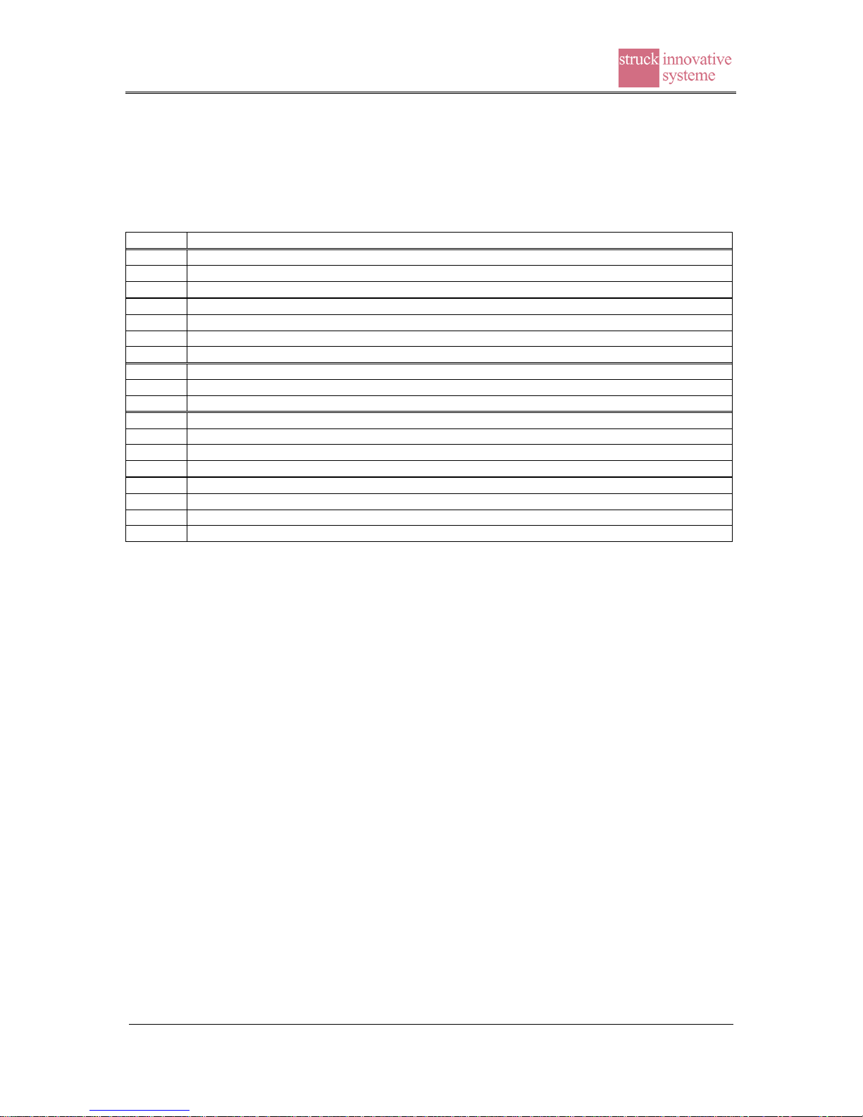
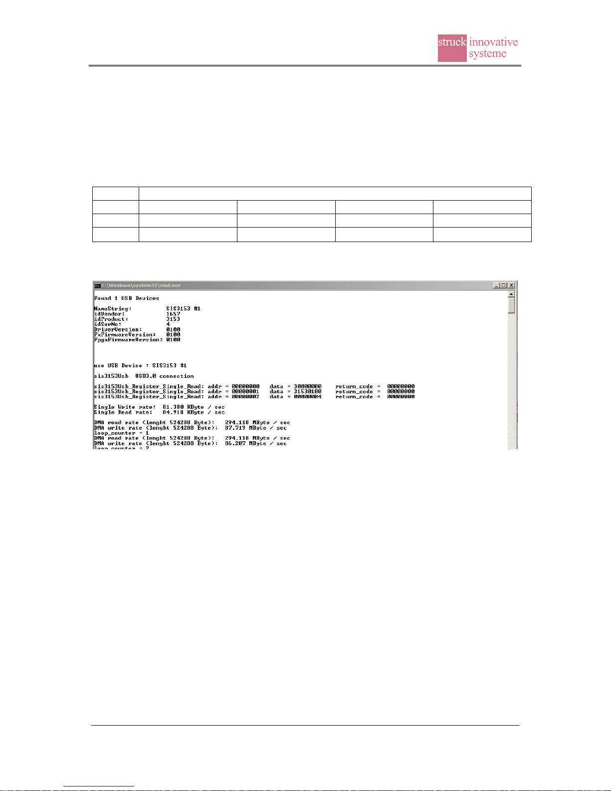
4.1 USB –SIS3153 Internal Space Data Rate
appr. continuous Data Rate
Single Data Write
DMA Block Write
Single Data Read
DMA Block Read
USB2.0
15 KByte/sec
20 MByte/sec
15 KByte/sec
40 MByte/sec
USB3.0
82 KByte/sec
87 MByte/sec
84 Kyte/sec
294 MByte/sec
Struck Documentation
SIS3153
VME interface
Page 20 of 38
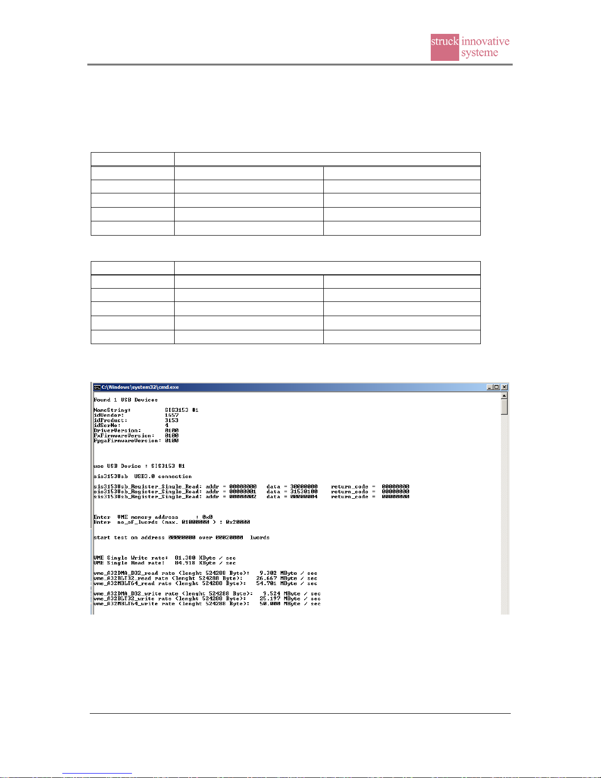
4.2 USB –SIS3153 VME Space Data Rate
4.2.1 VME Data Rate measured with a Chrislin VME Memory
USB2.0
approximate continuous Data Rate
Write
Read
A32-D32
15 KByte/sec
15 KByte/sec
A32-DMA-D32
9 MByte/sec
9 Myte/sec
A32-BLT32
19 MByte/sec
25 Myte/sec
A32-MBLT64
19 MByte/sec
39 Myte/sec
USB3.0
approximate continuous Data Rate
Write
Read
A32-D32
81 KByte/sec
84 KByte/sec
A32-DMA-D32
9 MByte/sec
9 Myte/sec
A32-BLT32
25 MByte/sec
26 Myte/sec
A32-MBLT64
50 MByte/sec
54 Myte/sec
Screen shot of the test program with USB3.0 connection.
Note: The Chrislin memory is a legacy card, which does not have a state of the art VME slave
implementation, but provides means to test standard read/write cycles like A32 D32.
Table of contents
Popular Recording Equipment manuals by other brands

SMAR
SMAR PCI302 Operation, maintenance & instruction manual

VTC Pro Audio
VTC Pro Audio DLMS4080 Connecting

RME Audio
RME Audio ADI-2 user guide

Axxess
Axxess AX-CH5-SWC installation instructions

Sound Performance Lab
Sound Performance Lab 9737 owner's manual

HMS Networks
HMS Networks Intesis INMBSMIT001I000 manual


