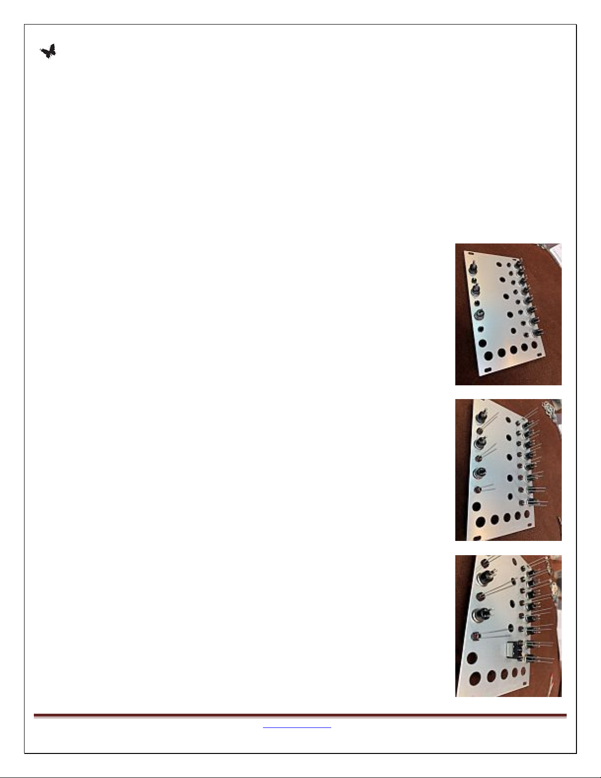
I. Overview/Features
This module is a rhythmic step sequencer. Sequences are programmed by using push
buttons to turn the steps on or off. Two sequences are output simultaneously while only one at a
time can be edited, a toggle switch selects which output is being edited. It features EEPROM
storage of patterns, and sequences up to 32 steps long.
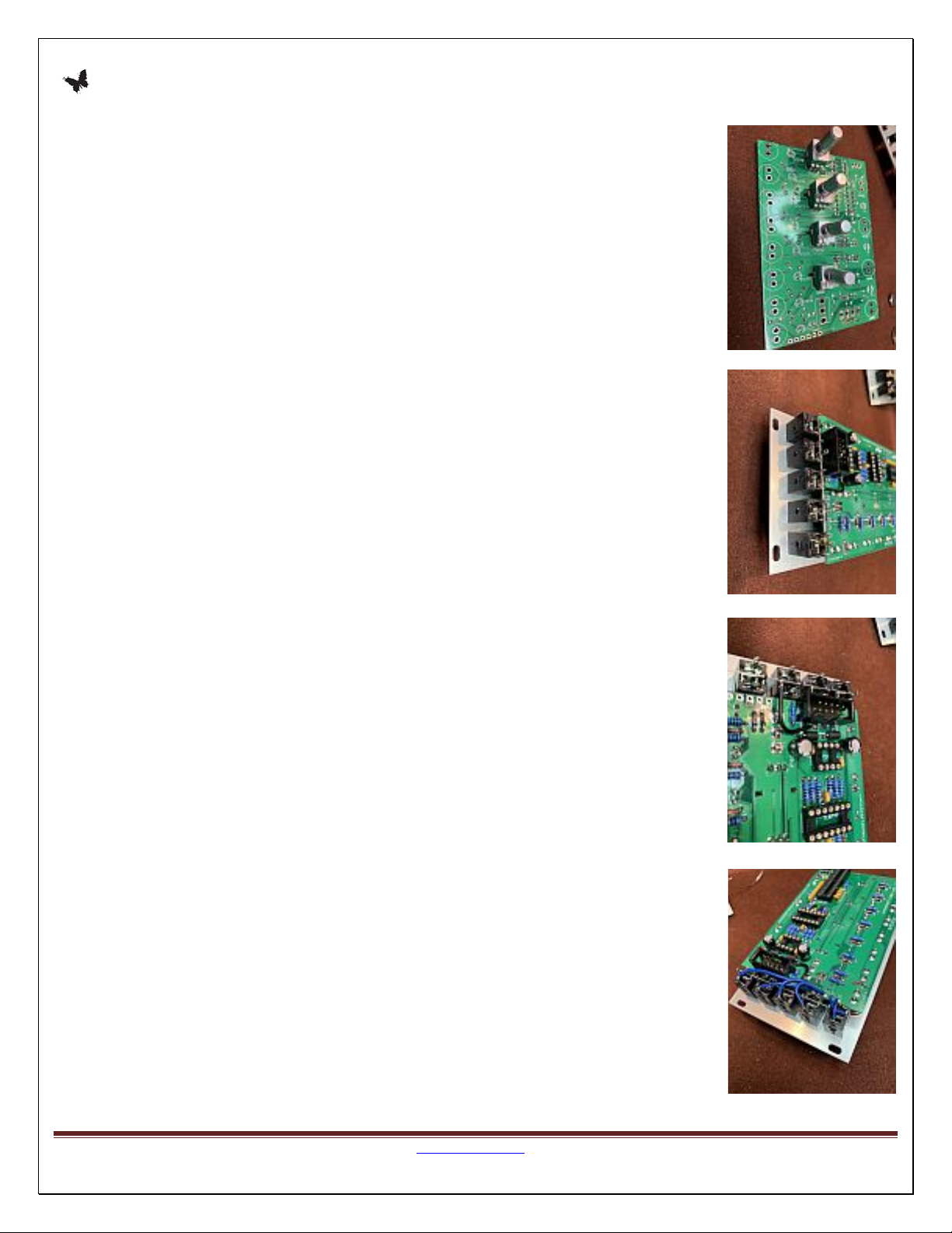
CONTRO S
1.Step on/off buttons – These are the 8 buttons which turn individual steps of the pattern on or off.
The LEDs next to the buttons indicate whether the step is on or off.
2.Speed Knob – This controls the speed of the internal clock. When an external clock is input, this
knob controls a divider for the external clock, dividing by 1, 2, 4 or 8.
3.Page Knob – Because there are only 8 buttons used to control up to 32 steps, this knob selects
which steps are being edited. When the sequence length is set to 8 or less, this control does nothing.
4.Length Knob – This sets the length of the sequence. Available lengths are 2, 4, 8, 16 and 32. This
control and the Page knob affect both sequences simultaneously.
5.Bank Knob – This selects which bank is being used for the SAVE and LOAD functions. There
are 5 available banks to save/load.
6.Edit Toggle – This selects which channel is being edited. When the switch is down Output 1's
sequence is being edited, and when up, Output 2's sequence is edited.
7.Erase Button – This button erases the current sequences.
8.Reset Button – This button will return the sequences to the first step on the next clock input.
9.Save Button – This saves the current sequences to the selected bank.
10.Load Button – This loads the sequences selected by the bank knob. If the selected sequence's
length is different from the length currently selected by the Length knob, it will override the length
knob until the length knob is adjusted.
INPUTS
1.Clock input – An external clock can be applied to this input.
2.Reset Input – This input works in parallel with the Reset Button, when the input goes high the
next clock tick will go to the first step of the sequence.
OUTPUTS
1.Clock Output – This outputs triggers in time with the clock.
2.Output 1 – This outputs triggers for sequence 1.
3.Output 2 – This outputs triggers for sequence 2.