Takenaka System TL-5150S User manual

1/ 13 (ver.0.1)
Model: TL-5150S
TAKENAKASENSOR GROUP
TAKENAKA SYSTEM CO.,LTD.
□
H e a d O f f i c e
86-66 Nomizo-cho Otsuka Yamashina-ku 607-8135 Kyoto JAPAN
TEL:+81-75-593-9300 FAX +81-75-593-9790
□
I n s p e c t i o n S y s t e m D e p t .
86-66 Nomizo-cho Otsuka Yamashina-ku 607-8135 Kyoto JAPAN
TEL:+81-75-593-9300 FAX +81-75-593-9790
□
C a m e r a D e p t .
4F Matsumasa Bld.1-17-14 Ogaya Otsu Shiga 520-2144 JAPAN
TEL:+81-77-545-4331 FAX +81-77-545-4335
□
T o k y o O f f i c e
2F MK Bldg. 2-2-19 Sotokanda Chiyoda-ku 101-0021 Tokyo JAPAN
TEL :+81-3-3255-0361 FAX:+81-3-3255-0362
TAKENAKA SYSTEM CO.,LTD. URL http://www.takex-system.co.jp/
TAKENAKA SENSOR GROUP URL http://www.takex.co.jp/
Line scan camera
Instruction Manual

2/ 13
Table of Contents
1. Outline ………………………………………………… 4
2. Features ………………………………………………… 4
3.Applications ………………………………….…………… 4
4.Specifications …………………………………………… 4
5. Camera I/O ……………………………………………… 5
5-1. Power source
5-2. I/O connector
6. Timing chart ……………………………………………… 7
7. Exposure control ……………………………………………… 8
8. Illustrative drawing of internal structure and switches ……………………………… 10
9. Notes ……………………………………………… 12
10. External dimensions ……………………………………………… 13

3/ 13
● Note that the contents of this manual are subject to change without notice for improvement.
● All contents of this manual are subject to the copyright owned by Takenaka System Company.
Unauthorized copy inhibited.
The Brief History of Takenaka System Co.
Takenaka System Co.(Trade mark:TAKEX) is the Japan’s first company to have produced the Line scan
cameras. It was established in 1975 and began to produce and sell the Line scan cameras that year.
And then, Takenaka System Co. is continuing to produce high quality line scan cameras such as C-MOS/
CCD Line scan cameras, CCD Analog line scan cameras, CCD Digital line scan cameras and CCD Camera
Link line scan cameras, as a pioneering company in the Japanese industry,.
Also, Takenaka System Co. began to produce the compact CCD video cameras since 1983, and is a first
producer of Full frame shutter cameras (Progressive scan camera) in Japan.
We think it is a mission of our company to continue to provide the high-quality Line scan cameras and Full
frame shutter cameras to the industry as image input device for image processing apparatus.
We are confident that the Takenaka’s products that met the strict performance test criteria are assured of
trouble-free operation over a long period of time.

4/ 13
1. Outline
●TL-5150S is the high-resolution Digital Line Scanner equipped with CCD linear image sensor.
●Digital video signal (10 bit) and analog video signal (0 to 2.5V at 75Ω-terminated) are delivered at a time as in
the case of UFD series camera.
●High-resolution and High-speed CCD Line Scan Camera featuring 5,150 image pixels and 40MHz data rate.
2. Features
●Encoder input operation is getting easier because the simplified exposure control function is incorporated.
●Sensitivity(GAIN) can be changed from 50V/Lux・sec to 400V/Lux・sec in 8 steps.
●The equipment operates with a single DC12V power source.
●Best suited usage for different purpose is feasible as the GAIN setting can be changed in the x1 to x 8
sensitivity range.
●A pixel size is small enough (7μm×7μm) to capture high-definition images.
3. Applications
●Image processing device for Image inspection.
●Measuring equipment such as appearance inspection or various dimensional measurement system
●Surface inspection apparatus of sheet-like object .
●Pinhole detector
4. Specifications
Number of pixels
5150
Pixel size
7μm ×7μm
Photo array length
36.05mm
Data rate
40 MHz (Max)
Scan rate (scan/sec)
250 to 7510 Hz
Clock pulse : Pixel data
1:1
Minimum number of clock pulses
5326
Driving clock pulse input
20/40MHz RS644 100Ωterminated
Driving clock pulse output
RS644
Line transfer pulse input
0.133 to 4 msec RS644 100Ωterminated
Line transfer pulse output
RS644
Video output (Analog output)
(Digital output)
0 to 2.5V (at 75Ωterminated)
Digital video signal (DO0to DO9) (RS644)
Sensitivity
50V/lx.sec (at GAIN 1)
Saturated exposure amount
0.08 lx.sec
Dynamic range
1000 (standard)
Output ununiformity
10% Max.
at 50% of saturation output
Power supply
+12V ±0.2V (420mA)
Operational ambient temperature
0~+40℃
Operational humidity range
85%Max.
Storage temperature range
-10℃~+65℃
Weight
Approx. 500g
Lens mount
Asahi K mount (standard)
Nicon F mount (optional)
External dimensions (mm)
64(W) ×64(H) ×88.8(D)

5/ 13
5. Camera I / O
5-1 Power source
Power is supplied through 15 pin connector. Though ripple-free and stable power source is preferable, the
switching supply is also employable. In general, ripple voltage of a stabilized power source is approx.35mV, and
approx.120mV for a switching supply. As voltage ripple is added to video signals, S/N ratio degrades when ripple
voltage is too large.
When more than one line scanner is connected to a single power source, be sure to keep cables from varying
extremely in length. When cable length varies greatly depending installation location of line scanner and power
source, use multiple small-capacity power sources.
5-2 I/O connector
●Spectral sensitivity
Connector panel
DIGITAL OUT connector(36pins)
SYNC connector
Analog VIDEO connector
Exposure control switch
POWER connector Power indicator
(15pins)
VIDEO
SYNC
DIGITAL OUT
POWER
EXP
Wavelength(nm)
1.0
0. 8
0 .6
0.4
0. 2
40 0 500 6 00 7 00 80 0 90 0 10 00
0
Relative sensitivity
(Typical value)

6/ 13
●Power connector [Dsub 15pins male]
●DIGITAL OUT connector [HIROSE: DX20A36S]
●SYNC connector……Connector for monitoring internal SYNC signal
It can be monitored by oscilloscope.
Signal level is TTL level.
Pin No.
Signal name
Pin No.
Signal name
1
SHIELD
9
NC
2
+12V
10
GND
3
GND
11
NC
4
NC
12
SYNCIN
5
SYNC+ IN
13
CLOCKIN
6
CLOCK+ IN
14
SYNCOUT
7
SYNC+ OUT
15
CLOCKOUT
8
CLOCK+ OUT
Pin No.
Signal name
I/O
Pin No.
Signal name
I/O
1
CLK+
Out
2
CLK-
Out
3
SYNC+
Out
4
SYNC-
Out
5
6
7
GND
8
GND
9
EX CLK+
In
10
EX CLK-
In
11
EX SYNC+
In
12
EX SYNC -
In
13
14
15
DO0+
Out
16
DO0-
Out
17
DO1+
Out
18
DO1-
Out
19
DO2+
Out
20
DO2-
Out
21
DO3+
Out
22
DO3-
Out
23
DO4+
Out
24
DO4-
Out
25
DO5+
Out
26
DO5-
Out
27
DO6+
Out
28
DO6-
Out
29
DO7+
Out
30
DO7-
Out
31
DO8+
Out
32
DO8-
Out
33
DO9+
Out
34
DO9-
Out
35
GND
36
GND
Power connector pin assignment
(Pin arrangement viewed from
the outside of the camera)
1
15
8
9
CLK…… Pixel clock
SYNC……Synchronizing signal
DO0~DO9…Digital video out

7/ 13
6. Timing chart
E XT SY NC In
E XT CL K In
S YN C O ut
Pulse width of SYNC:100nsec or more
(EXT CLK 20MHz or more)
D ATA
D ATA C LO CK Ou t
56 CLK
Removal period 5nsec
DATA setup time 12.5nsec±3nsec
S 1
100 CLK
S 2
S 3
S 4
E XT CL K In C LK du ty r ati o M in 40 %, Ma x 6 0%
D ATA C LO CK Ou t C LK du ty r ati o M in 35 %, Ma x 65 %
TL-5150S Timing Chart
Detailed Chart
EX CLK In
EX SYNC In
SYNC Out
D.CLK Out
Mi ni mu m ou tp u t pi xe ls (53 2 6C LK )
DATA
D2 7
D2 8
S 5 1
S2
S1
D7 4
D7 2
D7 3
S 5 1
S 5 1
S 5 1
S 5 1
2 6C LK
D7 6
D7 5
D7 8
D7 9
D8 0
D8 1
D9 4
D2 6
D u mm y si gn al (7 4p ix el s )
Op ti ca l b la ck (4 8p ix e ls )
1
3
5
7
59
D2 5
D2
D1
159
157
155
D2 9 113
111
109
85
61
5303
5305
5307
5309
5328
Du mm y si gn a l
(24 画 素 分 )
56 CL K
Ef f ec ti ve p ix el si gn al

8/ 13
7. Exposure control
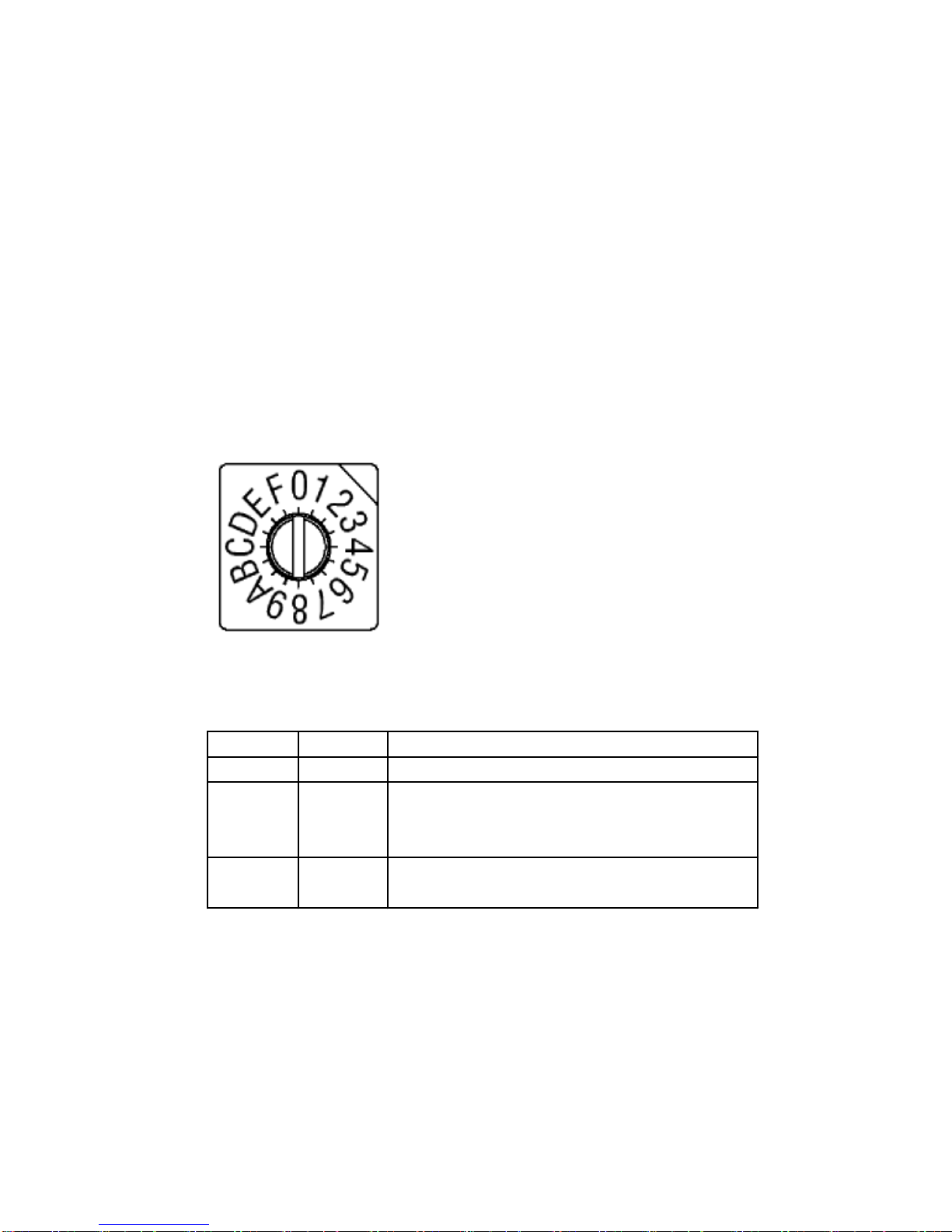
It can switch between three types of Exposure control modes by manipulating EXP switch (Exposure control switch)
on the rear panel.
①Line period exposure (at scan rate 7.54kHz or less) EXP setting N=0
Exposure during each period of EXT SYNC
②Fixed time exposure (at scan rate 3.7kHz or less) EXP setting N=1 to E
Exposure during the period of the equation below
from the timing of leading edge of EXT SYNC
Exposure time= 25.6 × N + 40 clk (μsec )
③Pulse width exposure (at scan rate 3.7kHz or less) EXP setting N=1 to F
Exposure during the period o f the pulse width of EXT SYNC
Exposure time = H period of SYNC + 40 clk –6clk
<Illustrative drawing of EXP switch>
Dial reading
0
1
~
~
E
F
Exposure during the period
where EXT SYNC is in H level
PULSE
Contents
Mode
LINE
FIX1
~
FIX14
Exposure during each period of EXT SYNC
Exposure time: 25.6 μs x 1+1μs
Exposure time: 25.6μs x 14+1μs

9/ 13
ST O UT -1
EXT.SYNC IN
SYNC OUT
Fixed time exposure (SW=N、N=1 to E)
E xp o s ur e du r in g th e p e ri od of th e e qu a ti o n be l ow
f r o m t h e ti m in g of l ea d in g ed g e o f E X T .S Y N C( C C1 ) .
E x p os u r e ti m e= D at a ou t d u r at i o n + 2 5 . 6 ×N ( μs e c )
M in i m um e xp os u re ti me = D a ta ou t d ur a ti on
* N ot e t h at th e m in i mu m p er i od o f E X T. S YN C i s
Da ta ou t d u ra ti o n ×2 i n t he Fi xe d t i me e x po s ur e m od e .
S T- 1
Exposure tim e
S T- 1 DA TA o ut d ur at io n
ST -2 S T- 3
Exposure time
ST O UT -2
Exposure time
S T- 2 DA TA ou t du ra ti on
DATA
Pulse width exposure (SW=N、N=F)
E xp o su r e du r in g t h e pe r io d o f t he pu ls e w i dt h o f E XT . SY NC ( CC 1 ).
M i m i mu m e x po s u r e t i m e = D at a ou t du r at i o n
* N o te th at th e m i ni mu m p e ri od of EX T. S YN C i s
Da ta ou t d ur a ti o n ×2 i n t h e P ul se wi d th e x po s ur e m od e .
SYNC OUT
DATA
EXT.SYNC IN
S T- 1
Exposure t ime
S T- 2 DA TA o ut d ur at io n
S T OU T- 2S T OU T- 1
S T- 1 DA TA o ut d ur at io n
Exposure time
S T- 2
Exposure t ime
S T- 3
Line period exposure (SW=0)
E xp os u re du ri n g e ac h p er i od of E X T. S YN C
DATA
SYNC OUT
ST -0 D AT A
ST O UT -1
EXT.SYNC IN
Exposure t ime
S T- 1
ST -1 D AT A
S T OU T- 2
S T- 2 DAT A
S T OU T- 3
Exposure time
S T- 2 ST -3
Exposure tim e
S T- 3 DA TA
S T OU T- 4
ST -4

10 / 13
8. Illustrative drawing of internal structure and switches
(A) Side view of internal structure
PCB2-CN6
PCB2-CN6
PCB1-VR1
(B) Side view of internal structure
PCB2-SW1
Gain selector switch
PCB2-SW1 ON OFF
1 to 3 in SW1
123
OFF
OFF
OFF
ON
OFF
OFF
OFF
ON
OFF
ON ON
OFF
OFF
OFF
ON
ON
OFF
ON
OFF
ON ON
ON ON ON
Enlarged view
4 to 7 in SW1(Unused)
8 in SW1
OFF:Automatic change to SYNC
PCB1-VR1
EVEN Gain adjusting VR
ON:Fixed to EXT SYNC
x8
x4
x5
x6
x7
Gain
x1
x2
x3
Connector for

11 / 13
(C) Top view of internal structure
PCB3-VR2
PCB3-VR1
PCB3-VR2 WC level adjusting VR
PCB3-VR1 Black level adjusting VR
PCB4-SW2 External input selector switch
15pin Connector/36pinConnector
Selector switch
For EXT SYNC and CLK input
PCB4-SW2
Digital out Power
Connector connector
(36 pins) (15 pins)
Connector panel side
Sketch drawing of the Switch

12 / 13
9. Notes
Precautions for use
■Do not make an impact on the equipment.
■Do not lag the equipment with heat insulating agent. If the equipment is covered with heat insulating agent, It
produces an increase in temperature and it causes the equipment to malfunction.(except for low-temperature
environment use)
■Take appropriate measures such as heat removal or cold removal to prevent dew condensation, when to move It
to the place where temperature difference is extremely severe. Usage with dew condensation causes the
equipment to malfunction.
■When the equipment is not used for a long time, protect the imaging device from dust or scratch by attaching a
lens cap. Do not store the equipment at the following places.
・The place where is subjected to a lot of dust and moisture.
・The place where is subjected to direct sunlight.
・The place where is extremely hot or cold.
・The place in the vicinity of an object which generates intensive electromagnetic field.
・The place where is subjected to intensive vibration.
■Please wipe off the dirt on the lens surface with a cotton swab preventing scratch to the lens surface.
Use a soft cloth to clean up the camera body.
■Use the equipment with a voltage within the range of specifications and do not connect the equipment to a power
source that contains intense noise components. In such case, the image output from the camera may contains
noise components.
■Do not use the equipment in an environment subject to intense electromagnetic field.
In such an environment, malfunction of the camera, disturbance of image and noise are caused by the field.
■In case of the high-intensity object, it may happen that even the low intensity part is displayed whitely like a
vertical streak above and below the high-intensity object. This phenomenon is called “smear”. However it is the
problem specific to CCD and it is not the camera-related failure.
■In case of the linear object, jagged picture may be displayed. Also in case of the pinstripe or checkered pattern,
annual rings- like picture may be displayed. However these are also the problem specific to CCD and it is not the
camera-related failure.
■The lighting using a commercial power source may cause a perceptible flicker at higher shutter speed.
In cases like this, consider to adjust shutter speed setting of the camera or to use the DC lighting or high-
frequency lighting.
Attention
■All rights on this manual reserved.
■The specifications and operational details described in the manual are subject to change for performance
improvement or other reasons without notice.

13 / 13
10. External dimensions
E l e m e nt
S YNC VI DEO EX P
D IG IT AL O UT
PO WER
( F o u r f a c e s )
6
6 8 . 2
6 3 . 5
8 6 3. 5
2 7 . 6
φ6 3
φ6 3 . 8
1 1 . 2 1 7 . 5 1 7 . 5
3 0 . 5
K- M o u n t
M 2. 6 De pt h6
2 - M 6 D e p th 8
1 / 4- 2 0 U N C D e p th 8
F B : 4 5 . 5
( 19 .3 )
1 8
8 7 . 5
Table of contents
Other Takenaka System Digital Camera manuals