Taxan Ergovision 740 LR User manual
ee
oe
coueal!’
Game!
Ges.
Se
Ae
ee,
TY
L
hex
oe
Brertincs
TPAXAN
Document
Title:
Ergovision
740
LR
&
740
TCO
Service
Manual
001
Nigel
Inkson
issue
Number:
Issued
By:
Revisions:
001
Original
Issue
22/05/96
Document
Control
Date
of
Issue:
22/05/96

oe
on
ee
|
th
i
f..
ee
ee
ee
bbvssrene
ie
Safety
Standards
and
Approvals
This
monitor
complies
with
DHHS
Rules
21
CFR
Subchapter
J
Applicable
at
date
of
manufacture.
Certified
to
comply
with
che
limits
for
a
Class
B
computing
device
pursuant
to
part
15
of
FCC
rules
Please
refer
to
instructio~s
included
FCC
notice
in
the
user’s
manual
if
this
equipment
is
suspected
of
causing
interference
tc
radio
reception.
Important
Safety
Notice
This
equipment
conizins
special
components
which
are
important
for
safety.
These
critical
parts
should
only
be
replaced
with
the
parts
specified
by
the
manufacturer
in
order
to
prevent
X-radiation,
shock,
fire
or
other
hazards.
Do
not
modify
the
orginal
design.

Mi
Preface
i
Before
You
Start
General
Safety
Precautions
1.
Use
an
isolation
transformer
in
the
power
line
and
AC
supply
to
troubleshoot.
2.
When
servicing,
observe
the
original
lead
dress,
espe-
cially
in
the
high
voltage
circuits.
If
a
short
circuit
is
found,
replace
all
parts
which
have
been
overheated
or
damaged.
3.
Before
turing
the
display
on,
measure
the
resistance
between
B+
line
and
chassis
ground.
Connect
the
nega-
tive
side
of
an
ohmmeter
to
the
B+
fines
and
the
positive
side
to
chassis
ground.
Each
line
should
have
more
resisstance
than
the
following
specifications:
|
+200V
134.5KQ
|
}
TV
60.51KQ
(eee
ees
ee
ee
PER
Bak
|
+15V
27.13KQ
|
4.1502
4.
Potentials,
as
high
as
26kV
are
present
when
this
display
is
in
Operation.
Operation
of
the
display
without
the
rear
cover
involves
the
danger
of
a
shock
hazard
from
the
display
power
supply.
Servicing
should
not
be
at-
tempted
by
anyone
who
is
not
thoroughly
familiar
with
the
precautions
necessary
when
working
on
high
volt-
age
equipment.
Always
discharge
the
anode
of
the
pic-
ture
tube
to
the
display
chassis
before
handling
the
tube.
5.
After
servicing,
be
sure
to
check
the
items
listed
in
the
Safety
Checkout,
below
before
returning
the
serviced
unit
to
the
customer.
Safety
Checkout
The
following
checks
must
be
made
after
correcting
the
original
service
problem
and
before
the
unit
is
returned
to
the
customer.
1.
Check
the
area
of
your
repair
for
unsoldered
or
poorly
soldered
connections.
Check
the
entire
board
surface
for
solder
splashes
and
bridges.
2.
Check
the
inter
board
wiring
to
ensure
that
no
wires
are
pinched
or
coated
with
high-wattage
resistors.
3.
Check
that
all
control
knobs,
shields,
covers,
ground
Straps
and
mounting
hardware
have
been
replaced.
Makde
absolutely
sure
you
have
replaced
all
the
insula-
tors.
4,
Look
for
any
unauthorized
replacement
parts,
particu-
larly
transistors,
that
may
have
been
installed
dueing
a
previous
repair.
Point
them
out
to
the
customer
land
recommend
their
replacement.
5.
Look
for
parts
which,
though
functioning,
show
obvious
signs
of
deterioration.
Point
them
out
to
the
customer
and
recommend
their
replacement.
6.
Check
the
line
cord
for
cracks
and
abrasion.
Recom-
mend
the
replacement
of
any
such
line
cord
to
the
customer.
7.
After
making
any
repair,
check
the
B+
and
HV
to
see
whether
they
are
at
the
values
specified.
Make
sure
your
instruments
are
accurate;
if
your
HV
meter
always
shows
a
low
HV,
check
the
meter
to
ensure
it
is
not
malfunctioning.
8.
Carry
out
the
leakage
current
checks
as
detailed
below
overleaf,
Leakage
Current
Cold
Check
1.
Unplug
the
AC
cord
and
connect
a
jumper
between
the
two
prongs
on
the
plug.
2.
Turn
on
the
display
power
switch.
3.
Use
an
ohmmicter
to
measure
the
resistance
value
be-
tween
the
jumpered
AC
plug
and
cach
exposed
metallic
cabint
part
on
the
display,
such
as
scre«heads,
terminals
control
shafts,
etc.
When
an
exposed
metallic
part
has
a
return
path
to
the
chassis,
the
reading
should
be
between
240k
and
5.2M.
When
exposed
mets:
does
not
have
a
return
path
to
the
chassis,
the
reading
must
be.
vy
i,

Leakage
Current
Hot
Check
1.
Plug
the
AC
cord
into
the
AC
outlet.
Do
not
use
an
isolation
transformer
for
this
check.
2.
Connect
a
1.5k,
10
watt
resistor
in
parallel
with
a
0.15F
capacitor
between
each
exposed
metallic
part
on
the
set’
and
a
good
earth
ground
(see
How
to
Find
a
Good
Earth,
below)
as
shown
in
the
diagram
below.
Leakage
Current
Hot-Check
Circuit
AC
VOLTMETER
oY
—~O
o
0.15nF
=
MW
15002,
10W
To
instrument's
—*
exposed
metal
parts
Example
of
Leakage
Current
Hot-Check
Circuit
Good
earth
ground
3.
Use
an
AC
voltmeter
with
1000
ohms/volt
or
more
sensitivity
to
measure
the
potential
across
the
resistor.
4.
Check
each
exposed
metallic
part,
and
measure
the
voltage
at
each
point.
5.
Reverse
the
polarity
of
the
AC
plug
in
the
AC
outlet
and
repeat
the
above
measurements.
6.
The
potential
at
any
point
should
not
exceed
0.75
volt
RMS.
A
leakage
current
tester
(Simpson
Model
229,
RCA
WT-540A
or
equivalent)
may
be
used
to
make
the
hot
checks.
Leakage
current
must
not
exceed
0.5
milliamp.
Ifa
measure-
ment
is
outside
of
the
specified
limit,
there
is
a
possibility
of
a
shock
hazard
and
the
monitor
should
be
repaired
and
re-
checked
before
it
is
returned
to
the
customer.
How
to
Find
A
Good
Earth
A
cold
water
pipe
is
a
guaranteed
earth
ground;
the
cover
plate
retaining
screw
on
most
AC
outlet
boxes
is
also
at
earth
ground.
If
the
retaining
screw
is
to
be
used
as
your
earth
ground,
verify
that
it
is
at
ground
by
measuring
the
resistance
between
it
and
a
cold
water
pipe
with
an
ohmmeter.
The
reading
should
be
zero
(0)
ohms.
If
a
cold
water
pipe
is
not
accessible,
connect
a
60-100
watt
trouble
light
(not
a
neon
lamp)
between
the
hot
side
of
an
AC
power
receptacle
and
the
retaining
screw.
Try
both
slots,
if
necessary,
to
locate
the
hot
side
of
the
line.
The
lamp
should
light
at
normal
brilliance
if
the
screw
its
at
ground
potential
Trouble
light
Mie
Ohmmeter
AC
Wall
Socket
Cold
water
pipe
How
to
Check
for
Earth
Ground

Table
of
Contents
[Section
1)
Product
Specification
1.1.Monitor
Control
Locations
&
Functions
.
2...
0
ee
ee
ee
1-1
1:2:Product
Overview.
6.6
eck
a
ee
Re
te
ew
Oe
Ee
1-2
1:3:CRT
Characteristics:
«ise
sok
Zak
de
Ae
OE
ee
SR
1-2
44.
Power
SpeciliGations:
o.&
%-%.4
a
wi.
cameta
Ae
he
Ge
eae
eee
we
ewe
GAS
1-2
PVA
ATPOWErSUDDIV:
4.
Gas
GE
eee
Reh
Be
ae
ee
a
ee
Ee
ew
S
1-2
1.4.2.PowerManagement
...
0...
2
1-2
1.5.Video
Specifications.
2
0.
ee
1-2
1.5.1.Video
Amplifier
Performance.
........
Rade
eae
ba
Ses
eh
det
va
a
Meee
a
Peery
Gack
1-2
1.5.2.Video
Input
Signal
Characteristics
..
0.
0
ee
ee
1-2
1.6.Syne
Inpub’Signal
Characteristics:«-
«
x-y.4.4
ste
aw
G
hee
oh
ok
eA
ge
we
1-2
Os
Separate:
Synce
sei
2
cet
neta
we
Ea
a
een
Ohne
aint
AO
ee
1-2
4:
6:2.Composite:Sync.
sk
sce
eta
wa
RB
a
ek
ee
ede
1-2
16:3:;Syne-On-Greens:..4,
ats.
isk
a
ee
ees
PS
Posed
Sah
eee
he
Ae
ae
ee
1-3
Te7-Environmentalis
25.4.
248
ae
ee
a
ae
ER
Ae
te
en
Ae
ee
ee
1-3
1.7.1.Temperature/Humidity/Altitude
.......
teddies
ee
ates.
tf
oe
a
eas
1-3
1752
Vibration
Test.
sa
vee
ised
Gea
we
AA
oe
we
ene
ek
be
ae
Gee
1-3
TFS
sDIOD
MOS
4:
ate
te
ok
Aad
va
GE
ee
ee
Ee
OT
a
1-3
1.8.Preset
Timing
Modes
.
2...
1-3
[Section
2.
Disassembly
Instructions
2.1.Removing
the
Rear
Cover
2.
10.
2-1
2.2.Remove
Top
Shield
and
Rear
Shield...
2...
2
ee
ee
2-1
2.3.Internal
Disassembly
(Right
Side).
2
2
2
2-1
2.4.Internal
Disassembly
(Left
Side)
.
2...
ee
2-1
2.5.Removing
the
Neck
Board
&
Main
Board...
1...
es
2-2
2.6.Remove
the
Control
Board
..
2...
2.
2-2
[Section
3,
Theory
of
Operation
3.1
ySwitehing
Power
Supply”
4.02
4.0.
2g
Aes
ieee
A
Eb
be
Be
a
ee
et
3-14
Sol
WwAUtO-degauSsing:
6...
ad
ota
aoe
Sayer
ae
Sl
be
ae
aes
we
deat
ed
3-2
3.1.2.Suspend
Mode
Operation
..
1...
3-2
3.2.The
Deflection
Circuit.
2.
3-2
3.2.1.16301
LM1291
Video
PLL
System
for
Continuous-Syne.
2...
ee
3-2
3.2.2.1C301
LM1291
Pin
Descriptions
..
2...
2.2...
ee
3-4
3.2.3.1C302
LM1295
DC
Controlled
Geometry
Correction
System
2...
2.
...02..
3-5
3.2.4.1C302
LM1295
Pin
Descriptions
..
2...
ee
3-5
3.2.5.Vertical
Deflection
Circuit.
2.
0
2
2
ee
ae
ee
ee
ee
3-6
3.2.6.Geometry
Correction
Circuit
2...
3-7
3.2.7.Structure
of
Horizontal
Deflection
Circuit.
2
2
ee
3-7
3:2.8.X-RAY
Protection:
Citeult
.205
cee
ew
op
a
we
ee
3-12
S279:
The
FOCus
Circuit
oa
sye,
oe
ier
Bel
a
eS
OH
ad
ee
he
Sd
A
3-12
EV740LR
Service
Manual
Table
of
Contents
/
1

3.2.10.Horizontal
linearity
and
CS
Switching
|
.
3.3.Video
Amplifier...
2...
002,
3.4.Microprocessor
And
Sync
Processing
......
.
Section
4
Setup
Adjustments
4.1.Preparing
the
Display
for
Adjustment
...
2...
4.1.1.Test
Equipment
Required...
0.0.2.2...
4.2.Adjustment
Procedures
........020022..,
4.2.1.Adjustment
Sequence
...........,
4.2.2.Preset
Timings
Used
During
Adjustment
4.3.High
Voltage
Verification...
.......022.
4.4.G1
Voltage
Adjustment...
.....000000.
4.5.Background
Brightness
Setting
..........
4.6.Screen
Brightness
Adjustment...
.....020..,
4.7.Magnetic
Field
Configuration.
.......20202..,
4.8.Raster
Center
Verification
.......0002,
4.9.Tilt
Verification
2.2.0.0...
.000000000,
4.11.Color
Misconvergence
.............
4.12.Primary
Test
Mode
Performance
Adjustments
.
4.13.Performance
Adjustments
for
All
Preset
Modes
4.14.lmage
Performance
Verification
..
2.0.0...
4.15.Uniformity
Verification.
.
2...
4.16.Brightness
Verification
Hg)
FN
Ae
we
ae
4.17.Display
Size
Stability
2...
000.0000
20.,
4.18.Color
Purity
Verification...
2...
4.19.Video
Noise...
.
2...
ee
4.20.Power
Saving
Check
.........,..0.2..
4.21.DDC
1/2
Data
Writing...
2...
[Section
5.
Troubleshooting
5.1.No
Display
at
Power-on
..
2...
.0.020002..,
5.2.No
X-ray
Operation...
2...
2...
5.3.No
Video
Operation
........0..00020..
5.4.Poor
VerticalLinearity
..........0.00.,
5.5.Poor
Horizontal
Linearity...
2...
2
5.6.Poor
Uniformity...
5.7.Tilted
Display
Area...
5.8.Misconvergence
............0.....,
5.9.Poor
Regulation
.
2...
00000020204,
5.10.PoorFocus
...............0.
0...
[Section
6,
Printed
Circuit
Boards
6.1.Neck
Board...
.....02.2.20,022..,
6.2.Main
Board
......2.2.,20202202..,
2/
Table
of
Contents
6:3:
Control:
Board’
ss
sch.
acee
y,
ae
a
we
Bah
Soe
IS
al
ak
ae
a
Se
6-3
6.4.PCB
Wiring
Connection...
2.
ee
6-3
Schematic
Diagrams
7.1.Video
Circuit
Diagram
.
6.
1
toluene
7-1
7.2.Deflection
&
S/P/S
&
Logic
Circuit
Diagram...
2...
ee
ee
7-1
Mechanical
Parts
Be
Key
to-Exolodad
Views
«oce's
ak:
b
Aes)
AR
a
ee,
©
OS
He
Be
a
OR
eS
8-1
6:2.Exploded
VieW:
25
Lak
lise
dete
ee
ae
a
ee
a
et
eed
ea
gS
he
8-2
[Section
9!
PCB
Component
List
9.1.Explanation
of
Parts
Listing...
ee
9-1
9:2"
Main
Board:
c.g
8
sara
Ce
acds
Foc
hee
A
ee
er
ee
ER
ae
ee,
ee
ee
te
9-1
9:9:Neck
Board!
2-23
oso.
Gls
8 a
Rte
ws
ate
a
ee
od
te
a
A
a
9-7
9:4.
Control:
Board.
2.3
05.
eo
ee.
te
SIS
ER
ey
Ge
oie
at
pe
he
eB
We
we
9-9
9.5.HITACHI
CRT
Different
List.
2.
2
2.
9-9
9.6.
TOSHIBA
CRT
Different
List
2...
2
9-9
EV740LR
Service
Manual
Table
of
Contents
/3
Notes
4/
Table
of
Contents
EV740LR
Service
Manual

~
Product
Specification
Tate
Monitor
Control
Locations
and
Functions
........-
1-1
1.2.
Product
Overview
...
2...
0.
cee
eee
eens
1-2
13;
CRT
CharacteristicS
..
0...
6c
cee
eee
eee
1-2
1.4.
Power
Specifications.
0.6...
.
eee
eee
eee
eee
1-2
1.5.
Video
Specifications
....
6...
cere
eee
eee
ees
1-2
1.6.
Sync
Input
Signal
Characteristics
........-..++-.
1-2
Tet
Environmental.
......00
00
ee
eee
eee
teenies
1-3
1.8.
Preset
Timing
Modes
......-.-.
seer
tress
1-3

EV740LR
Service
Manual
:
:
:
1.1.
Monitor
Control
Locations
&
Functions
TAXAN
crconsion
rin
laongs
‘s
Set
\
EPA-POLLUTION
PREVENTER
SELECT
aDjUST
f
N“N
v4
és
7s
c
}
Se
7
N
x
“N
4
~~
4
_~
Y
XS
/
SS
DEG
SELECT/
CED)
ei
Oo
|
:
|
ies
ae
rae)
:
©
|
|
KEY
TO
BUILT-IN
MONITOR
CONTROL
FUNCTIONS
Manual
Degauss
and
Ractery.
Se
ing
Recall
unction
Digital
control
for
manual
degauss
of
monitor
at
the
normal
condition
and
for
recall
the
origional
factory
setting,
during
OSD
pattern
is
on
screen.
Thumbwheel
for
Adjusting
Setting
and
OSD
Function
Selection
Thumbwheel
for
adjusting
the
setting,
clockwise
for
increasing
and
counterclockwise
for
decreasing
and
selection
the
OSD
function
icon.
Push
Button
for
OSD
|
Press
to
call
up
OSD
function
into
screen
and
confirm
the
thumbwheel
ON/OFF
and
enter
for
icon.
Thumbwheel
Enter
Confirm
Increase
/
decrease
raster
black
level
using
thumbwheel
adjusting,
Brightness
Control
:
B
clockwise
for
increasing
and
counterclockwise
for
decreasing.
utton
Contrast
Control
Butto
Increase
/
decrease
video
gain
using
thumbwheel
adjusting,
clockwise
for
n
increasing
and
counterclockwise
for
decreasing.
Hard
power
On/Off
button.
Adjacent
LED
is
lit
when
on.
The
LED
color
is
green
for
normal
condition
and
change
to
orange
for
DPMS
condition.
—
Power
On/Off
1-1

:
Product
Specification
1.2.
Product
Overview
[]
EPA
energy
star.............
standby
<
30
watts
The
monitor
installed
in
the
EV740LR
(RMH
7H11)
phom
described
in
this
service
manual
has
the
following
features:
1.5.
Video
Specifications
O
17
inches
0.26mm
dot
pitch
conventional
CRT
1.5.1.
Video
Amplifier
Performance
30-85
kHz
horizontal
scanning
:
.
;
O
Bandwidth
(dot
rate).........
135MHz
O
Thirteen
preset
modes
:
:
;
;
O
Typical
10%~90%
rise
and
fall
times
calculation
5.5ns
1
Universal
segmented
auto
range
power
supply
: ;
;
;
.
O
Video
generator
rise/fall
times
.
2ns
maximum
O
VESA/NUTEK/EPA
compliant
power
management
;
O
Scope
and
probe
bandwidth
...
350MHz
minimum
41.3.
CRT
Characteristics
O
Probe
capacitance
...........
2.5Pf
:
O)
Overshoot/Undershoot
.......
10%
maximum
O
Screen
Size,............005.
17
inches
:
fC]
Sync
on
green
..............
Amphitude:714mV
O
Faceplate
Type............-.
Fs
maximum
Sync
on
Green
Amplitude:286mV
maximum
O
Orientation.............0045
Landscape
C
Phosphor
Dot
Pitch..........
0.26mm,
1.5.2.
Video
Input
Signal
Characteristics
delta
atvangement
a
:
O
Video
Type
................
Analog
Oo
aan
GUNG
edn
es,
ear
Fi
Amplitudes
ceneniucesley
ss
700mV
maximum
a
oe
etree
ae
:
cee
O
Video
Input
Impedance.......
75
Ohms+1%
cic
a
ee
1
Optional
DDC
1/2B
Video
Connector
Pin
Assign-
O
Phosphor
Type.............-
P22
fients:
CO
Phosphor
Persistence.........
Medium
Short
O
Faceplate
Properties..........
ASN
coating,
mn
on
nner
anti-static,
anti-reflection
|
pin.
Signal
|
O
Standard
Light
Transmission...
53.5%
Typical
Red
video
Bd
:
Sync
return
1.4.
Power
Specifications
Monitor
GND
12
|
SDA(bi-directional)
|
1.4.1.
Power
Supply
13
1H.
sync
O
A/C
Receptacle
..........-0.
1EC320
14
|V.
sync
(VCLK)
_|
O
Power
Supply
Type..........
Universal
|
15
[SCL
O
A/C
Line
Voltage
Ranges
.....
88VAC-132VAC
180VAC-264VAC
O
A/C
Line
Frequency
Ranges
...
50Hz/60Hz+3Hz
|
YOO®O®
O
Inrush
Current..............
30A/132V
or
|
©®O®O®
@
SOA/264V
(at
cold
start)
ig
Q®R
OG
O
Leakage
Current.............
<3.5mA
|
sai=s
=
O
Degauss
.............-.
000
Automatic
and
Manual
(20
minutes
for
a
full
recovery)
1.6.
Sync
Input
Signal
Characteristics
1.4.2.
Power
Management
Oo
Summary
of
operating
states:
1.6.1.
Separate
Sync
Automatic
O
Syne
Type
.......
2.2
eee
TTL
EE
ONELY
:
ad
Time
O
Amplitude
..............0.0.
2.4V
minimum
green
not
applicable
(Logie
High),
0.8V
max.(Logic
Low)
orange
<3
seconds
QO
Polartly
..
0.0.0.0...
ee
eee
Positive
or
Negative
orange
<10
seconds
(1
Equalization
pulses
..........
Not
allowed
orange
<10
seconds
Shan’
;
1.6.2.
Composite
Sync
|
green
not
applicable
" ;
;
mot
O
Syne
Type
......
62...
eee
TTL
O
Signaling
compliant
with
VESA
DPMS
guidelines
:
}
aot
O
Amphtude...........0..00.
2.4V
minimum
O
Nutek
1992
guidelines........
suspend
<
30
watts;
(Logic
High),
0.8V
max.(Logic
Low)
off
<
8
watts
EV740LR
Service
Manual
La
O
Polarity
................2..
Positive
or
Negative
O
Serration
pulses.............
Allowed
at
horizontal
rate
(
Equalization
pulses..........
Not
allowed
1.6.3.
Syne
On
Green
O
Syne
Type..............04.
As
per
Apple
O
Amplitude
.................
OV
min(Logic
High)
-286mV
max.(Logic
Low)
O
Polarity
................04.
Negative/Composite
Ol
Serration
pulses.............
Allowed
at
horizontal
rate
O
Equalization
pulses.......,..
Not
allowed
1.7.
Environmental
1.7.1.
Temperature/Humidity/Altitude
OPERATING
O
Temperature..........
10°C
to
35°C
O
Relative
Humidity
.....
0
to
90%,
non-condensation
O
Altitude
.............
NON-OPERATING
0
to
10,000
feet
O
Temperature..........
-40°C
to
+65°C
‘O
Relative
Huntidity
.....
0
to
95%,
non-condensation
O
Altitude
.............
0
to
40,000
feet
Vibration
Test
UNPACKED
UNIT
1.7.2.
Operating
without
package:
|__|
Frequency
|
|_i_|
5:22
|
22-500Hz
Times/Cycle:
Amplitude
Acceleration(G)
O
Rise
Time..................
10
Minutes
O
Fall
Time..................
10
Minutes
O
Number
of
Sweeps
..........
I
Cycle
EAS
Soa
eile
aes
ten
tieat
X,Y,Z
C
Total
Times
................
60
Minutes
PACKAGED
UNIT
Storage
with
package:
Acceleration(G)
|
0.83G
Amplitude
Frequency
5-5O0Hz
Times/Cycle:
O
Rise
Time...........0..00.,
10
Minutes
O
Fall
Time........0.....0...
10
Minutes
1-3
O
Number
of
Sweeps..........
1
Cycle
ED
AXIS
oes
pices
eons
bee
ke
a
eed
X,Y,Z
O
Total
Times................
60
Minutes
1.7.3.
Drop
Test
O
Compliant
with
NSTA
Project
1A
guidelines
O
Drop
Height
...............
46cm
O
Test
Direction..............
1.8.
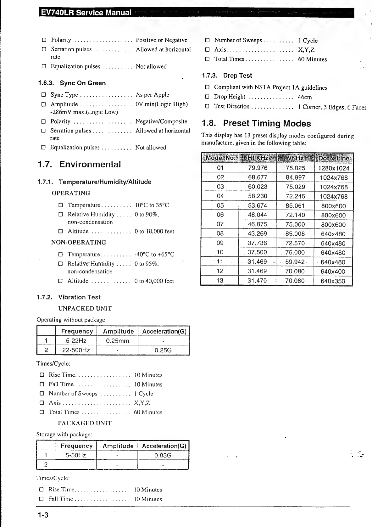
Preset
Timing
Modes
This
display
has
13
preset
display
modes
configured
during
manufacture,
given
in
the
following
table:
eDoti
1280x1024
|
1024x768
1024x768
1024x768
800x600
800x600
800x600
|
43.269
640x480
_|
|
_o9
37.736
640x480
_|
640x480
640x480
|
12
31.469
640x400
31.470
640x350
_|
68.677
60.023
58.230
53.674
48.044
46.875
‘3
CINE
Be
j=)
jee)
1
Corner,
3
Edges,
6
Faces
_
ss
Disassembly
Instructions
—
2A;
Removing
the
Rear
COVE
sd
aN
Million
Dawe
Ota
kes
6
2-1
22.
Removing
the
Top
Shield
and
Rear
Shield........
2-1
2.3,
Internal
Disassembly
(Right
Side)...............
2-1
2.4.
Internal
Disassembly
(Left
Side)................
2-1
2.5.
Removing
the
Neck
Board
and
Main
Board
2.6.
Removing
the
Control
Board................05.
2-2
3
EV740LR
Service
Manual
;
2.1.
Removing
the
Rear
Cover
1.
Remove
the
four
screws
at
the
rear
of
the
display.
Refer
to
the
figure
2-1
(A).
2.
Remove
the
rear
cover.
Figure
2-3
Remove
the
Top
Shield
&
Rear
Shield
2.3.
Internal
Disassembly
(Right
Side)
The
neck
board
is
plugged
on
to
the
CRT
neck
and
is
enclosed
in
a
metal
shielding.
1.
Disconnect
the
two
ground
wires.
Refer
to
the
figure
2-4
(A).
2.
Remove
the
connected
pin
from
the
Neck
Board.
Refer
to
the
figure
2-4
(B).
Figure
2-1
Remove
the
Rear
Cover
3.
Remove
the
two
connected
pins
from
the
Main
Board.
Refer
to
the
figure
2-4
(C).
2.2.
Remove
Top
Shield
and
Rear
_
4.
Remove
the
connected
pin
from
the
Main
Board
to
Control
Board.
Refer
to
the
figure
2-4
(D).
Shield
5.
Remove
the
two
screws
at
the
bezel.
Refer
to
the
figure
1.
Disconnect
the
five
ground
wires
from
the
top
shield.
2-4
(E).
Refer
to
the
figure
2-2
(A).
=
A)
6.
Remove
the
nylon
revets
holding
from
Bezel.
Refer
to
2.
Remove
the
two
screws
at
the
top
shield.
Refer
to
the
the
figure
2-4
(F).
figure
2-2
(B).
3.
Disconnect
the
two
ground
wires
from
the
top
shield.
Refer
to
the
figure
2-3
(A).
an
ze)
a
4,
Remove
the
two
screws
at
the
top
shield.
Refer
to
the
figure
2-3
(B).
]
5.
Release
the
cord
cramp
from
the
top
shield.
Refer
to
the
figure
2-3
(C).
6.
Remove
top
shield
and
rear
shield.
Figure
2-4
Internal
Disassembly
(Right
Side)
2.4.
Internal
Disassembly
(Left
Side)
=~
1.
Disconnect
the
ground
wire.
Refer
to
the
figure
2-5
(A).
2.
Remove
the
connected
pins
from
the
Main
Board.
Refer
Figure
2-2
Remove
the
Top
Shield
&
Rear
Shield
to
the
figure
2-5
(B).
2-1
rs
Ss?
Disassembly
Instructions
IMPORTANT
NOTE
To
avoid
risk
of
electric
shock,
before
re-
moving
the
anode
cap,
made
sure
tdhe
an-
ode
has
been
completely
discharged
as
high
voltage
may
remain
on
the
anode
for
extended
time
after
power
off.
3.
Remove
the
anode
cap
from
the
CRT.
Refer
to
the
figure
2-5(C).
4.
Remove
the
two
screws
at
the
bezel.
Refer
to
the
figure
2-5
(D).
5.
Remove
the
nylon
revets
holding
from
bezel.
Refer
to
the
figure
2-5
(E).
Figure
2-7
Remove
the
Control
Boaed
Figure
2-5
Internal
Disassembly
(Left
Side)
2.5.
Removing
the
Neck
Board
&
Main
Board
1.
Disconnect
the
three
ground
wires
from
the
Neck
Shield.
Refer
to
the
figure
2-6
(A).
2.
Remove
the
neck
shield.
3.
Remove.the
Neck
Board.
4.
Remove
the
Main
Board.
2.6.
Remove
the
Control
Board
1.
Remove
the
four
screws
from
the
Control!
Board.
Refer
to
the
figure
2-7
(A).
2.
Remove
the
Control
Board.

EV740LR
Service
Manual
Notes
2-3
3.1.
3.2.
3.3.
3.4.
Theory
of
Operation
Switching
Power
Supply
The
Deflection
Circuit
Video:
AMDIING!
«40st
scan
ae
eat
eas
eee
eS
3-12
Microprocessor
and
Sync
Processing............
3-13

EV740LR
Service
Manual
_
|
3.1.
Switching
Power
Supply
The
switching
power
supply
(SPS)
used
in
this
display
is
a
150W
flyback
mode
type.
The
power
supply
provides
seven
outputs
(B+,
77V,
15V,
-15V,
6.3V
,415V
and
+5V).
Please
refer
to
schematic
diagram
for
details
of
the
circuit
layout.
The
input
voltage
is
from
88VAC
—
264VAC
with
an
input
frequency
of
47Hz
—
63Hz.
as
shown
in
figure
3-1.
The
current
first
passes
through
the
EMI
control
circuit
and
is
regulated
to
DC
by
the
bridge
diodes
(BD901)
and
filter
capacitor
(C907).
During
rectification
a
large
current
surge
is
generated
and
as
C907
has
a
very
low
impedance
while
being
charged
the
fuse,
on/off
switch
and
bridge
diode
are
all
liable
to
be
damaged.
Forthis
reason,
a
thermal
resistor
(NTCR)
is
added
before
the
bridge
diode
in
order
to
limit
the
large
current
surge
generated
during
the
charging
of
the
capacitor.
During
rectification,
C910
is
charged
through
R903
and
R904.
When
C910
is
charged
to
16V,
IC901
3842A
starts
to
operate
(for
details,
of
the
functions
of
this
IC,
please
refer
to
the
relevant
data
sheet)
and
outputs
a
pulse
signal
from
Pin
6
to
set
the
transistor
Q902
in
the
ON
state.
At
this
time,
transformer
T903,
which
is
connected
in
parallel,
starts
to
store
power.
When
the
current
passing
through
the
resistor
R914,
and
the
supplementary
current
from
R957
and
R964
into
Pin
3
of
IC901
reaches
1.1V,
IC9O1
is
reset,
causing
the
energy
stored
by
the
transformer
to
reach
the
rated
value.
In
order
to
prevent
the
transformer
from
being
saturated
and
causing
damage
to
the
transistor,
when
transistor
Q902
is
in
the
OFF
state,
the
energy
stored
in
the
transformer
T903
is
released
into
the
secondary
coil
and
is
regulated
through
the
various
output
loops
and
filters
and
converted
to
the
required
DC
output.
In
addition
to
this,
at
the
appropriate
time,
the
windings
pin!
—
pin2
supply
Pin
7
of
IC9Q1
with
a
fixed
power
supply
for
normal
operation.
Also,
when
windings
pin2
—
pin3
are
in
power
saving
active
state,
power
is
supplied
to
Pin
7
of
IC901
for
normal
operation.
In
any
of
the
above
cased,
the
output
pulse
is
terminated
and
the
FET
is
turned
off,
causing
the
voltage
on
the
output
of
the
FET
to
rise
rapidly,
and
the
voltage
across
the
winding
of
the
primary
to
reverse
in
polarity,
thus
tending
to
reset
the
flux
within
the
core.
At
this
point,
the
diodes
D915,
D925,
D917-
D920
and
D926
on
the
secondary
supply
winding
become
forward
biased
and
begin
to
conduct,
thus
transferring
energy
from
primary
to
the
secondary,
and
charging
the
secondary
capacitors.
There
is
also
secondary
winding
the
primary
side
of
the
power
supply
which,
through
diode
D908
and
Q901
recharges
the
control
IC901
reservoir
capacitor
C910.
This
supply
then
keeps
the
IC901
running.
In
the
event
of
a
secondary
short
circuit,
the
supply
fails
to
recharge,
thus
the
voltage
across
C910
drops
to
a
threshold
limit
below
which
the
[C901
cuts
out
and
returns
to
its
low
current
load
operation.
During
normal
operation,
the
supply
rails
charge
until
the
error
amplifier
realized
by
IC903
on
the
secondary
begins
to
turn
on
the
opto-coupler,
PH901.
At
this
point,
the
photo-tran-
sistor
of
this
opto-coupler
on
the
primary
side
begins
to
conduct,
draining
current
from
the
primary
control
IC901
supply
through
diode
D907
and
D928.
Under
normal
operation
IC903
regulates
the
current
flow
through
PH901,
and
hence
determines
the
output
voltage
of
the
error
amplifier
internal
to
IC901.
Various
passive
compo-
nents
around
[C903
and
IC901
set
the
gain
compensation
for
optimum
stability
and
regulation
characteristics.
In
the
event
of
a
fault
condition
occurring,
either
Q904
may
be
turned
on
by
the
lack
of
voltage
at
pin2
of
IC901
or
zener
diode
ZD903
may
conduct,
due
to
excessive
voltage
on
the
primary
IC901
supply.
In
the
latter
case,
the
triac
Q903
will
fire,
thus
dragging
down
the
output
of
the
control
IC901
error
amplifier,
which
in
turn
will
limit
the
duty
cycle
and
reduce
the
output
voltage.
It
will
stay
in
this
mode
until
the
AC
input
power
is
removed.
PMG1CONTROL
|.
FROM
LOGIC
CIRCUIT
PMG1———
CIRCUIT
Q905
weasel
ISOLATION
FEEDBACK
prea
Moe
Shoes
CIRCUIT
ats
CIRCUIT
[
PH901
1C903
|
loss
a
Bin
tel
FROM
FBT
oe
:
PULSE
SYNC
CIRCUIT
PWM
CONTROL
CIRCUIT
|
MAIN
SWITCH
30Khz~85Khz
‘|
Q907
a
UC3842A
(1C901)
Pe
_
qQg902
FUSE
Om
B5VAC~264VAC
AC
IVP
tp
Ue
EMI
CIRCUIT
T902
AUTO
OR
MANUAL
|!
|
DEGAUSSING
CIRCUIT
|
Q91i5,RL901
ft
j
FILTER
CIRCUIT
BD901
’
ee
te
PTV
I
Wid
ion.
te
eed
te?
>
15V
POWER
X'FORMER
O/P
RECTIFIER
pssy
12V
|
an
@EILTERS
eo
oeeeaesy
ae
|
———-+
CIRCUIT
|
|
NC
,
»
6.3V
ei
T903
Sy
|
»
5V
-
=»
B+
(200V)
Figure
3-1
Switching
Power
Supply
Block
Diagram
3-1
"e

i
Theory
of
Operation
When
the
feedback
signal
passing
through
the
main
77V
output
is
completed,
the
transistor's
duty
cycle
is
adjusted
through
the
transfer
to
Pin
2
of
IC901
3842A
of
the
primary
coil
by
PH901
4N35
and
IC903
TL431,
stabilizing
the
output
current.
At
this
time,
it
is
important
to
note
that
before
the
feedback
signal
is
established,
the
charge
level
of
C917
cannot
trigger
Q903
SCR
or
it
will
cause
a
faulty
power
startup.
In
addition,
in
order
to
synchronize
the
supply
power
and
moni-
tor
and
reduce
noise
that
will
cause
interference
to
the
display,
in
the
area
D913
the
monitor's
feedback
transformer
gets
a
feedback
signal
in
order
to
ensure
synchronization
between
the
power
supply
and
monitor,
with
synchronization
in
the
range
30kHz
—
85kHz.
Because
the
power
operating
fre-
quency
changes
with
the
monitor
causing
changes
in
the
value
of
IP,
(the
value
of
LP
is
fixed
while
the
value
of
IP
increase
or
decreases
according
to
the
frequency),
this
affects
the
test
value
of
Pin
3
of
IC901
3842A.
This
causes
the
total
power
supplied
to
vary
according
to
the
frequency,
so
a
compensa-
tion
value
is
provided
by
D914
in
order
to
reduce
the
differ-
ence
in
total
power
for
different
frequencies.
In
addition,
because
the
AC
input
ranges
from
85VAC
to
264VAC,
this
causes
the
value
of
the
direct
current
on
the
DC
bus
to
vary,
affecting
the
rise
rate
of
IP,
the
oscillator
and
the
duty
cycle,
and
causing
the
test
value
obtained
at
Pin
3
of
IC9O1
to
vary.
To
resolve
this,
a
compensation
value
is
provided
by
R964
and
R957
which
reduces
the
difference
resulting
from
the
different
input
voltages.
3.1.1.
Auto-degaussing
=
‘When
base
of
Q915
connector
is
in
high
state,
the
transistor
Q915
2SC945P
is
on,
causing
the
relay
to
jump
from
Normal
Open
(N.O.)
to
Normal
Close
(N.
C.):to
perform
auto-degaussing
operations.
The
du-
ration
of
this
operation
is
controlled
by
a
logic
pulse
and
lasts
approximately
6
(six)
seconds.
When
tran-
sistor
Q915
enters
the
OFF
state
and
the
relay
returns
to
N.O.
to
terminate
the
auto-degaussing
operation
is
completed.
3.1.2.
Suspend
Mode
Operation
Two
feedback
ratios
can
be
selected,
both
sensing
from
the
78V
rail.
In
the
event
of
Q905
being
turned
on
by
micro
processor,
additional
current
is
drawn
from
the
virtual
earth
node
of
IC903,
thus
causing
the
power
supply
to
serve
the
rail
to
a
high
voltage,
nominally
78V.
This
is
trimmed
by
resistor
R937,
R940
and
R941.
The
other
supply
raif
are
predeter-
mined
ratios
of
this
winging,
being
+15V,-
12V,+6.3V
and
+200V
nominally.
In
addition,
a
low
voltage
primary
side
winding
feeds
the
control
IC901
directly
through
D907
turning
off
the
control
[C901
supply
through
Q901,
which
would
otherwise
dissi-
pale
excessively.
When
Q905
is
turned
off,
the
78
V
rail
drop
to
around
17V.
In
this
case,
the
primary
control
supply
fed
through
D907
drops
to
a
value
that
is
below
the
level
needed
to
sustain
operation.
Instead,
Q901
begins
to
conduct
and
the
higher
voltage
supply
winding
taken
via
D908
is
used
to
keep
the
primary
side
powered
up
with
minimal
power
losses.
The
5V
power
supply
is
driven
by
one
of
two
sources,
In
normal
operation
when
the
78V
is
present,
the
5V_.
regulator,
IC902
is
fed
from
the
15V
rail
through
diode
D921.
When
switched
to
standby
mode
(78V
rail
drops
to
12V)
then
the
15V
rail
drops
too
low
to
supply
IC902.
In
this
case
Q906
take
over
and
main-
tains
the
supply
to
IC902
at
around
9V.
In
addition
to
the
5V
regulated
supply,
in
normal
operation
there
is
also
a
15V
regulated
supply
take
from
the
15V
rail.
To
ensure
that
micro
processor
gets
a
good
5V
power
supply,
there
is
a
power
good
detection
circuit
.
formed
by
Q801
and
Q802.
This
monitors
the
supply
going
into
the
5V
rail
(not
the
5V
rail
directly).
It
detects
whether
there
is
sufficient
voltage
to
enable
the
SV
regulator
to
work
effectively.
It
is
not
a
detection
of
the
5V
rail
itself,
but
relies
upon
the
premise
that
the
regulator
is
not
faulty
and
that
there
is
no
faulty
load
condition
on
the
5V.
During
power
up,
there
is a
delay
to
the
signal
at
the
output
of
the
threshold
comparator
Q801
and
Q802
a
caused
by
ZD801
and
C801,
in
order
to
allow
the
micro
Circuit
time
to
stabilize.
The
threshold
is
cho-
sen
such
that
the
RESET
line
drops
low
at
least
25ms
before
the
SV
drop
out
of
regulation.
—
L
Finally
a
synchronization
pulsé
taken
from
the’
oii
zontal
output
stage
maintains
the
SMPS
operating
frequency
in
sync
with
the
horizontal
scan.
D913
injects
a
pulse
which
prematurely
triggers
the
oscil-
lator
within
IC901
which
would
otherwise
run
at
a
frequency
lower
than
the
minimum
required
sync
frequency.
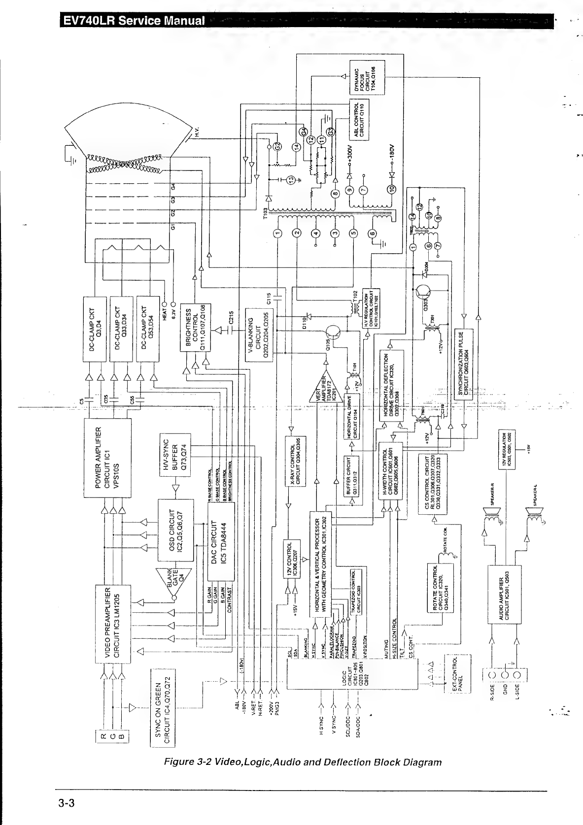
3.2.
The
Deflection
Circuit
Please
refer
to
the
block
diagram
of
the
deflection
circuit
and
video
circuit
and
Logic
circuit
as
shown
in
figure
3-2.
3.2.1.
IC301
LM1291
Video
PLL
System
for
Con-
tinuous-Sync
The
LM
[291
is
an
integrated
horizontal
time
base
solu-
tion
specifically
designed
to
operate
in
continuous-sync
video
monitors.
If
automatically
synchronizes
to
any
H
ferquency
from
30kHz
to
85kHz
and
provides
the
drive
pulse
to
the
high
power
deflection
circuit.
Available
sync
processing
includes
a
vertical
sync
sepa-
rator
and
a
composite
video
syne
stripper.
An
internal
syne
selection
scheme
giyes
highest
priorily
to
separate
Hand
V
syne,
then
composite
sync,
and
finally
syne
on
video,
no
external
switching
between
sync
sources
is
necessary,
The
LM1291
provides
polarity-normalized..*2
H/HV
and
V
sync
outputs,
along
with
logic
flags
which
show
the
respective
input
polarities.
The
design
uses
an
on-chip
FVC
(Frequency
to
Voltage
Converter)
to
set
the
center
frequency
of
the
VCO
a
a
a
a
3-2
EV740LR
Service
Manual
ee
yuaxvads
me
Aste
2OSO
“LSD
‘LOSd1
EOSD
'$0S91
LINDHID
af
Ono
<a
ae
Poa
ee
eee
=
walsngWy
o1lany
pee
wusyvaes
ic
L
-——<t-——
2
|
308-s
1
eeted
cst
—}-
the
it
¥09D'£090
LINDuia
i
1
3S1Nd
NOLLWZINONHONAS’
|
;
;
TBNV¢!
|
|
AOULNOD-L¥3
|
WOO
BivLOW
____
Hed
‘OREO
eee
ae
°
ney
ceed'zeeo'ree‘occo
Soe
nou
i
|
:
oi
toc
0Z€0'L0E'90£0'
LOE
Te
!
|
vege
rc0
06D
LINDYID
TONLNOD
SD
|
|
:
|
are
14ND
$5,
-
i
oles
Til
:
BOED'Z0ED
TOUINOD
SzIS-H
“OzEDt
LINDUID
BAwIO
:
NOILD31330
WWLINOZIMOH
JOYXLNOD
HLGIM-H
ONLLAA
5‘
ZOLLEOLD'L0151
byl
Li
|
BOLD
POLL
LINDUID
WOwLNOD
ahs
ji
:
LINDwID
NOLLYIADBY
A'H
[
7
a
ROUBOEA!
‘dochters
snoo4
OLLD
UNDUIS
:
COC
LINDuID
|
—o-<,
D00N0S
OINVNAG
|
|
TOXLNOD
TEV¥
i
Adle
{
revo
sinsuta)
-,
}
zeonico
|}
rOULNOD
OIOTBEVuL
|
-———sersaval
508-1081
<
BAINIG
TWLNOZINOH
LINDYID
W3IINE
|
~
—
Fi
UNIEID
|
.___<__
dganos
at
|
=e
OMTENDNTE
290)
PS
aanv
ve
x
[4
wo
se
rt
t
Reso
Weve
——I---
DNAS
A
Lhe
Fa
fbi
aistiawy}
|
ZOCOK'
LOCD!
TOWLNOD
AULINOZO
HIM
l
<
SAAS.
——<——
oNas
H
€3Al-
HOSS3I0Nd
TYOULWEA
¥
WLNOZINOH
|
<4
i
[ee
eS
Eee
ee
©
fe
A
1
Sare
:
SOED'POED
LINDUID
;
|
——~
sr
:
20Z0'9091
ASte
0G
TOS!
AOMINOD
AVE
YOULNOD
AZt
|
roe
J
-
i
|
ae
COW
1
-
=
A00z+
!
:
f
ar
—<—
LaaH
a
ee
pe
ADBL
>
Tey
TORINO)
SEIN
HONE
LSVYLNOD
i
Swath
brrSVaL
Sol
NIV
S
|
A
OUINGS
BSviE
5
‘
ecient
LINDYID
OVA
WOUINOS
FS
VIE
&
{
i
g
BOLD'ZOLO'LELO
|
Sa
———<}
TOULNOD
|
SSANLHOS
FLD
ELD
10'90'S0'291
LD
dAV19-50
yasane
->~
2
bb»
linoyioaso
|
|
ie
et
ONAS-/H
|
re
VV
VY
|
ZLD'OLD'FO!
LINDUID
|
|
N3BYD
NOONAS
|
saves
1
140
dwwI0-90
Vv
|
ere
=e
i
|
rea'eed
7
|e
1x9
diW10-00
z
SOLSGA
|
ly
GOZLWT
EDI
LINDUID
fs
ee
5
7
Lol
LINDUID
i
YBISIIdDWVSed
OSCIA
a1
y
|
ra'ed
1
|
UBIaMdWy
BaMOd
tote
clnat
m
Y
rae
so
|
-2
Video,
Logic,Audio
and
Deflection
Block
Diagram
Figure
3
3-3
This manual suits for next models
1
Table of contents
Other Taxan Monitor manuals


