Page 2 of 21
Document Number: DS-000358
Revision: 1.0
TABLE OF CONTENTS
General Description ..................................................................................................................................................................... 1
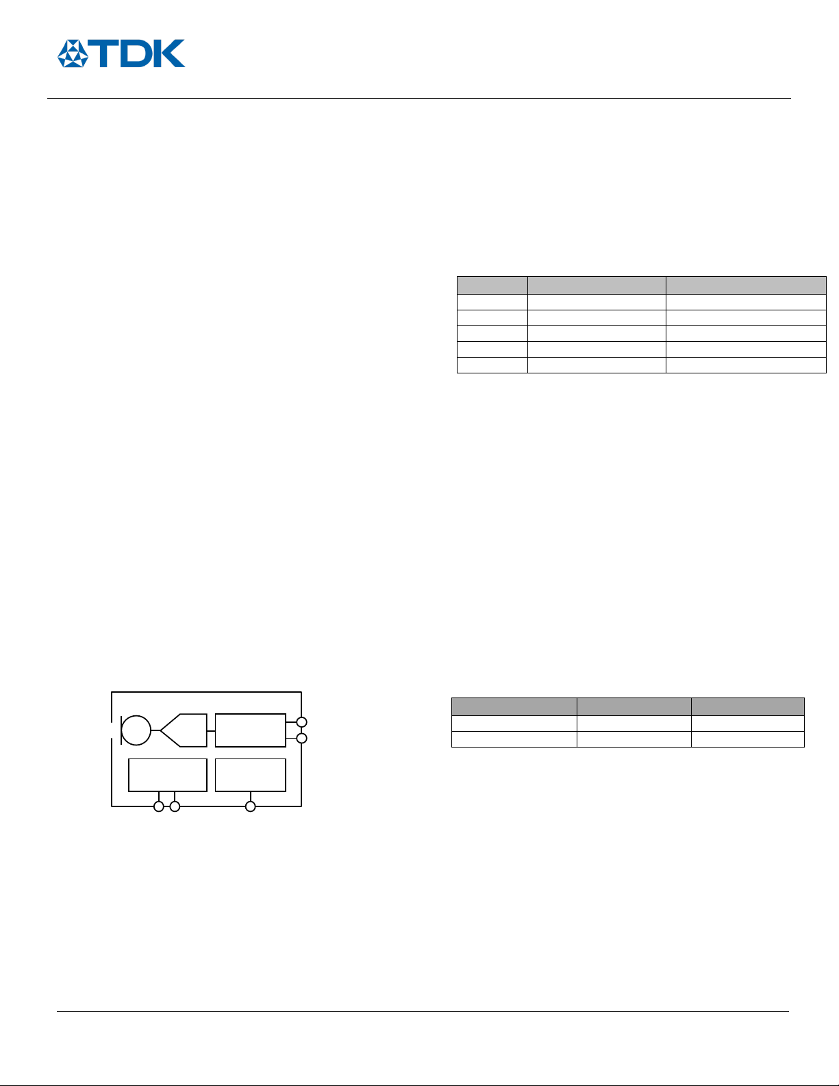
Functional Block Diagram ............................................................................................................................................................ 1
Applications ................................................................................................................................................................................. 1
Features ....................................................................................................................................................................................... 1
Ordering Information................................................................................................................................................................... 1
Table of Contents.................................................................................................................................................................................... 2
Specifications .......................................................................................................................................................................................... 4
Table 1. Acoustical/Electrical Characteristics – General.............................................................................................................. 4
Table 2. Acoustical/Electrical Characteristics – High Quality Mode ............................................................................................ 4
Table 3. Acoustical/Electrical Characteristics – Low-Power Mode.............................................................................................. 5
Table 4. Digital Input/Output Characteristics .............................................................................................................................. 5
Table 5. PDM Digital Input/Output.............................................................................................................................................. 6
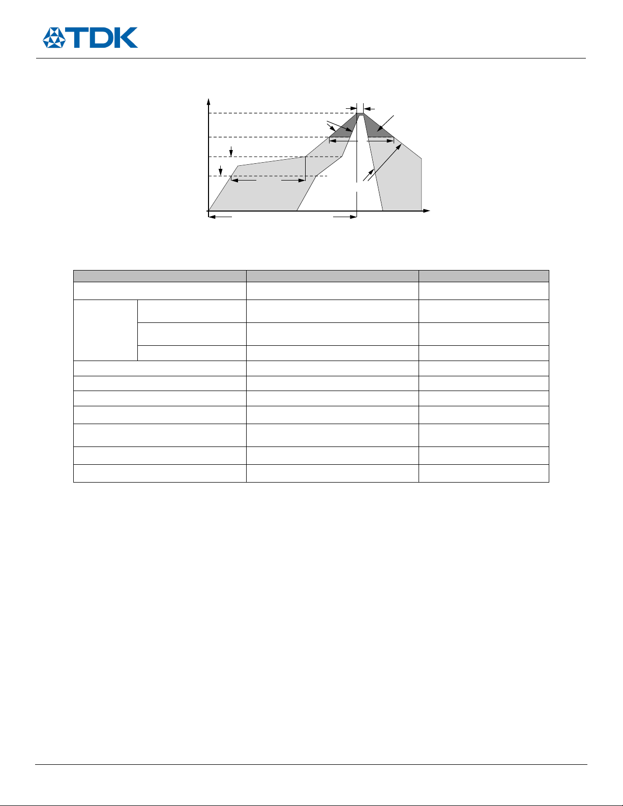
Timing Diagram............................................................................................................................................................................ 6
Absolute Maximum Ratings.................................................................................................................................................................... 7
Table 6. Absolute Maximum Ratings ........................................................................................................................................... 7
ESD Caution ................................................................................................................................................................................. 7
Soldering Profile........................................................................................................................................................................... 8
Table 7. Recommended Soldering Profile*.................................................................................................................................. 8
Pin Configurations And Function Descriptions ....................................................................................................................................... 9
Table 8. Pin Function Descriptions............................................................................................................................................... 9
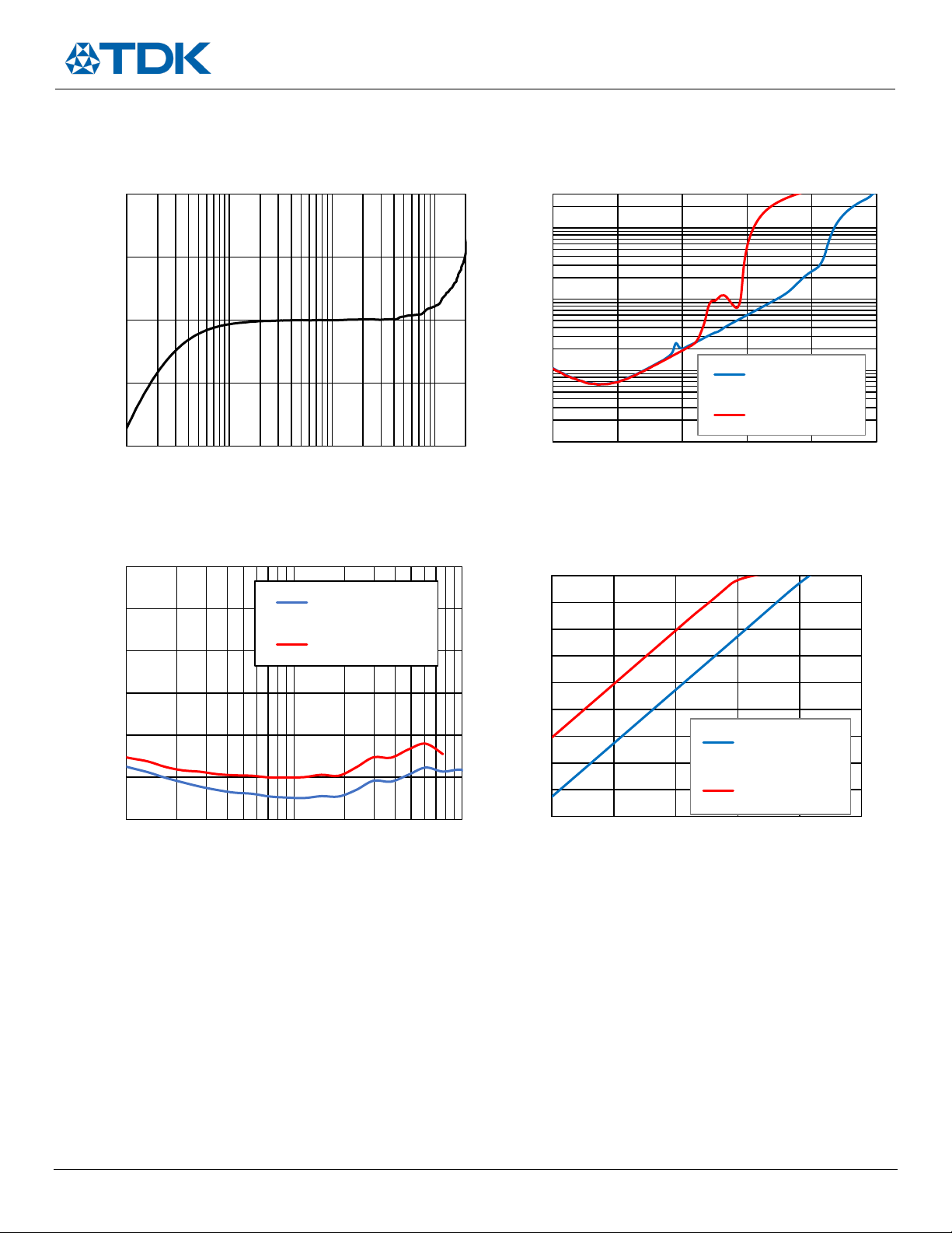
Typical Performance Characteristics..................................................................................................................................................... 10
Theory Of Operation............................................................................................................................................................................. 11
PDM Data Format ...................................................................................................................................................................... 11
Table 9. T3903 Channel Setting ................................................................................................................................................. 11
PDM Microphone Sensitivity ..................................................................................................................................................... 11
Applications Information ...................................................................................................................................................................... 13
Low-Power Mode....................................................................................................................................................................... 13
Dynamic Range Considerations ................................................................................................................................................. 13
Connecting PDM Microphones.................................................................................................................................................. 13
Sleep Mode................................................................................................................................................................................ 15
Start-Up Time............................................................................................................................................................................. 15
Supporting Documents ......................................................................................................................................................................... 16
Application Notes – General ...................................................................................................................................................... 16
PCB Design And Land Pattern Layout ................................................................................................................................................... 17
PCB Material And Thickness ...................................................................................................................................................... 17
Handling Instructions............................................................................................................................................................................ 18
Pick And Place Equipment ......................................................................................................................................................... 18
Reflow Solder............................................................................................................................................................................. 18