RS-M228X
CONTENTS
ITEM
PAGE
LOCATION
OF
CONTROLS
AND
COMPONENTS
------------
2
DISASSEMBLY
INSTRUCTION
--+----cseeers
sees
eeeee
te
teeee
ee
eees
3
MEASUREMENT
AND
ADJUSTMENT
METHODS
(without
dbx
SYSTEM)
‘ibietalerbisiaiolelala'e
einitie
slorw-sjateisiels
ewwle
eerie
viele
lois
5
MEASUREMENT
AND
ADJUSTMENT
METHODS
(for
dbx
SYSTEM)
(gE
ut
saiate
Syste
ySejeie
bie
ware
dig
915
olan
Cat
sigleieretelg
bate
ever
11
*
TROUBLESHOOTING
CHART
FOR
dbx
SYSTEM
----
11
*
ADJUSTMENT
PARTS
LOCATION
OF
dbx
SYSTEM
feesccceston
stoves
nnd
Sia
teowetnn
reduce
tet
ee
teenasiy
se
13
*
BLOCK
DIAGRAM
OF
dbx
SECTION
------+--eeeeeeeee
ee
13
*
dbx
SYSTEM
CHECKING
METHOD
..---------------e-5+
5
14
¢
ADJUSTMENT
OF
dbx
SYSTEM
--vecececececeeeeeeeeee
ees
15
*
CHECKING
PROCEDURE
FOR
PROBLEMS
-.----------
16
-
ELECTRICAL
PARTS
LOCATION
-:-:::ceccececeeeeeeteeeeeeneees
18
BLOCK:
DIAGRAM
2-:
seeds
eseeonseseocue
ttesseiag
sence
ecesce
vat
eecoess
20
ITEM
PAGE
SCHEMATIC
DIAGRAM
(MAIN/POWER
SUPPLY
SECTION)
----:++seereeeeeeeees
22
CIRCUIT
BOARDS
(MAIN/POWER
SUPPLY
CIRCUIT
BOARD)
----+-----
25
SCHEMATIC
DIAGRA
(dbx
SECTION)
---:-e:ceceseecee
eee
eeeeteeeeeeenteeneeeseereeeees
29
SCHEMATIC
DIAGRAM
(FL
METER
SECTION)
--c-eecceeeeece
eet
eceeseeeeeeeea
seen eres
30
CIRCUIT
BOARDS
(dbx/FL
METER
CIRCUIT
BOARD)
----:++-esreerrereees
31
WIRING
CONNECTION
DIAGRAM
.--eeeeeeeeeeeeeeeeneeer
tenes
33
CABINET
PARTS
LOCATION
<0:
-e:-sseececeeeeee
teste
eeeereeeaees
35
MECHANICAL
PARTS
LOCATION
-evcececcecececeteeeteeeeenee
37
MOTOR
UNIT
DISASSEMBLY
------:ereeceeteereeet
eee
eeteeea
ees
40
PRECAUTIONS
FOR
MECHANISM
UNIT
ASSEMBLY
----
40
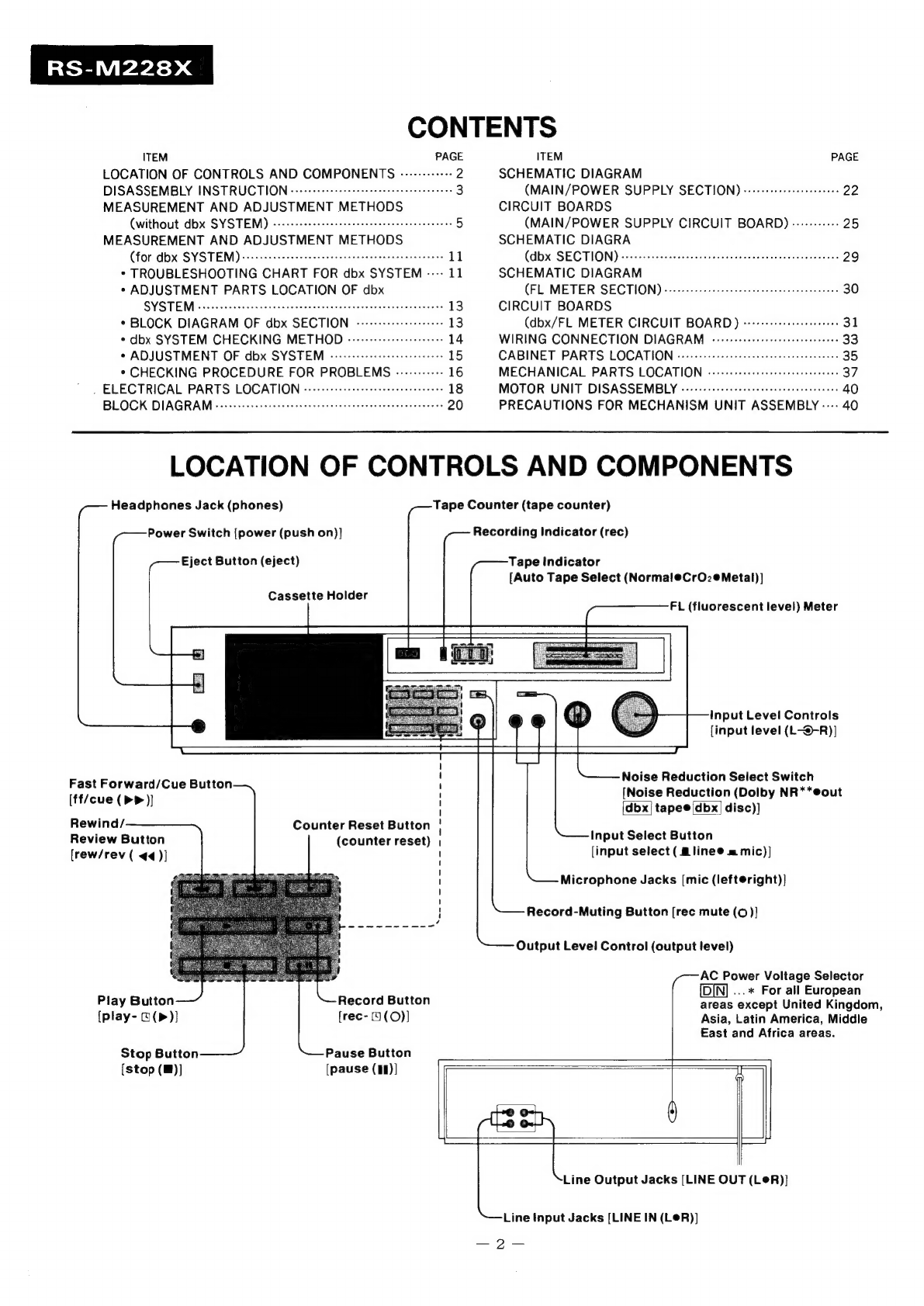
LOCATION
OF
CONTROLS
AND
COMPONENTS
Headphones
Jack
(phones)
Power
Switch
[power
(push
on)}]
Eject
Button
(eject)
Cassette
Holder
Tape
Counter
(tape
counter)
Recording
Indicator
(rec)
Tape
Indicator
[Auto
Tape
Select
(NormaleCrOzeMetal)]
FL
(fluorescent
level)
Meter
Input
Level
Controls
[input
level
(L-®-R)]
Noise
Reduction
Select
Switch
[Noise
Reduction
(Dolby
NR**eout
dbx]
tapee
(dbx|
disc)]
Fast
Forward/Cue
Button
[ff/cue
(>>
)]
Rewind/
Review
Button
{rew/rev
(
¢4)]
i}
i)
1
t
i}
1
Counter
Reset
Button
i
(counter
reset)
|
Input
Select
Button
i}
i]
i}
I
i}
!
!
i
¢
[input
select
(
@linee
=
mic)]
Microphone
Jacks
[mic
(left@right)]
Record-Muting
Button
[rec
mute
(0))
Output
Level
Control
(output
level)
(ea
he
Power
Voltage
Selector
[DIN]
...*
For
all
European
areas
except
United
Kingdom,
Asia,
Latin
America,
Middle
East
and
Africa
areas.
0
Record
Button
{rec-
9
(O)]
Play
Button
(play-
G(P))
Pause
Button
[pause
(1)]
Stop
Button
[stop
(@)]
;
Line
Output
Jacks
(LINE
OUT
(LeR)]
Line
Input
Jacks
[LINE
IN
(Le@R)]
—>
2
=—


