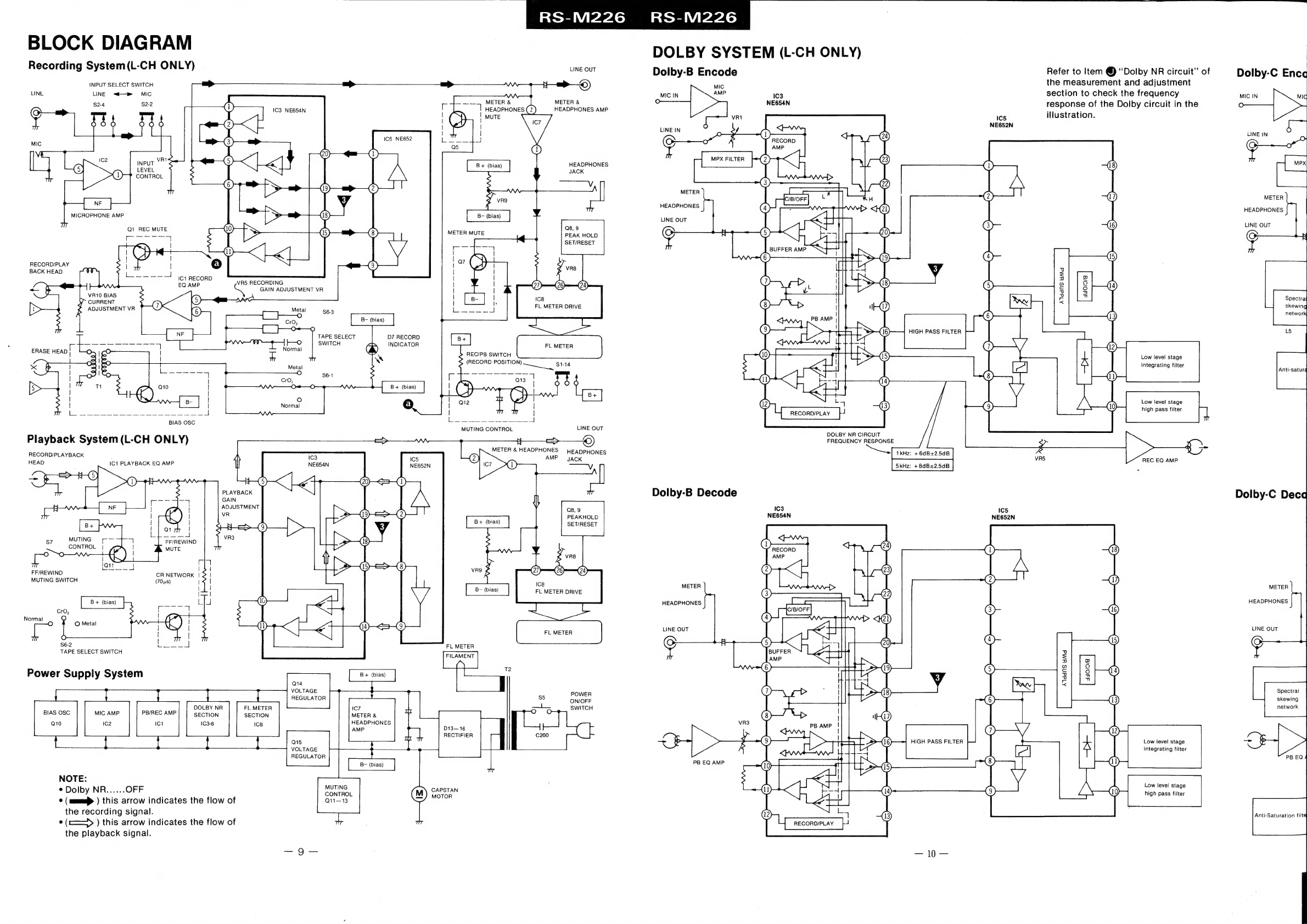
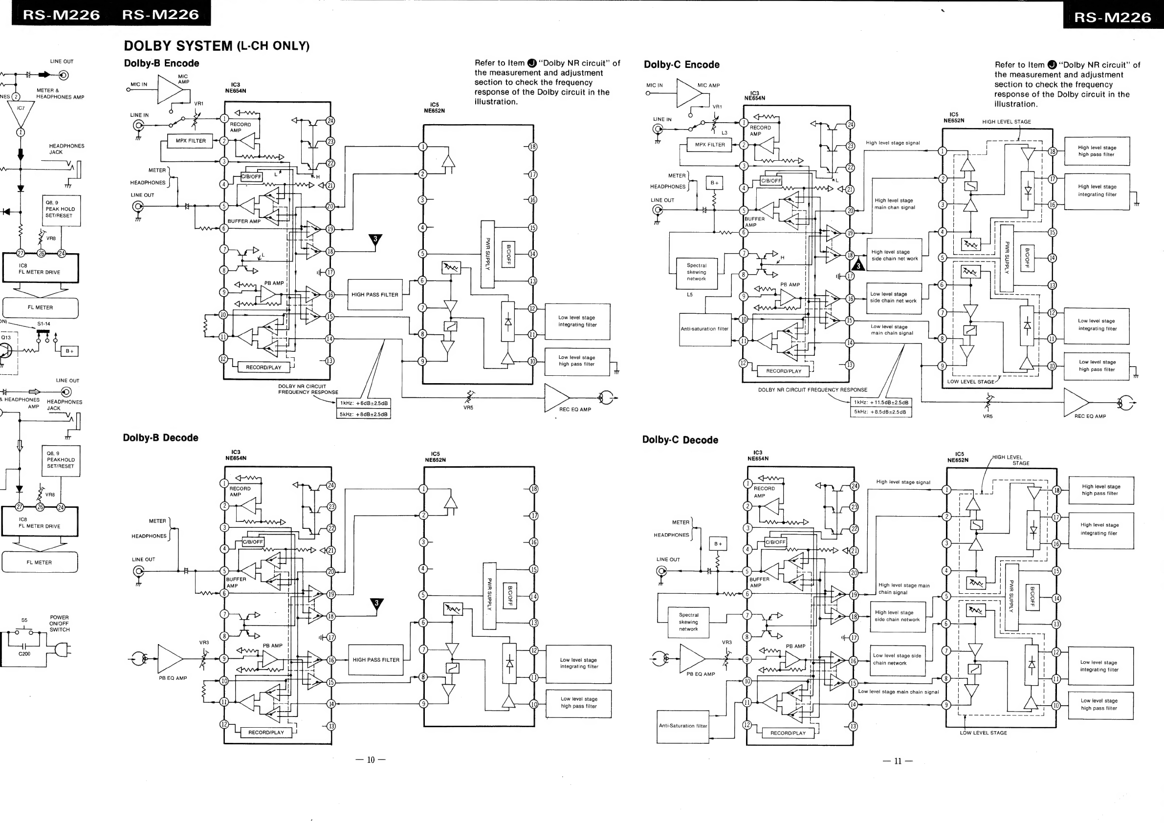
Technics RS-M226 User manual
Other Technics Cassette Player manuals

Technics
Technics RS-TR575 User manual

Technics
Technics RS-M228X User manual

Technics
Technics RS-TR165 User manual

Technics
Technics RSTR272 - DUAL CASS. RECORDER User manual

Technics
Technics RS-676US User manual

Technics
Technics RS-TR252 User manual

Technics
Technics RS-BX747 User manual

Technics
Technics RS-M85 User manual

Technics
Technics RS-TR333 - SCHEMATICS User manual

Technics
Technics RS-B605 User manual

Technics
Technics RS-TR232 User manual

Technics
Technics RS-CA01 User manual

Technics
Technics RS-AZ6 Quick start guide

Technics
Technics RS-TR979 User manual

Technics
Technics RSTR272 - DUAL CASS. RECORDER User manual

Technics
Technics RS-CH770 User manual

Technics
Technics RS-TR979 User manual

Technics
Technics RS-9900US User manual

Technics
Technics RS-CH700 User manual

Technics
Technics RS-TR474 User manual


Popular Cassette Player manuals by other brands


Sony
Sony CFS-B15 - Am/fm Stereo Cassette Recorder operating instructions

Sony
Sony WMFS220 - Portable Sports AM/FM Cassette... operating instructions

Aiwa
Aiwa HS-TA21 operating instructions

Sanyo
Sanyo MCD-ZX700F Service manual

Aiwa
Aiwa CS-P77 Service manual

Sony
Sony Pressman TCM-465V operating instructions