manuals.online logo
Brands
  1. Home
  2. •
  3. Brands
  4. •
  5. Technics
  6. •
  7. Stereo Receiver
  8. •
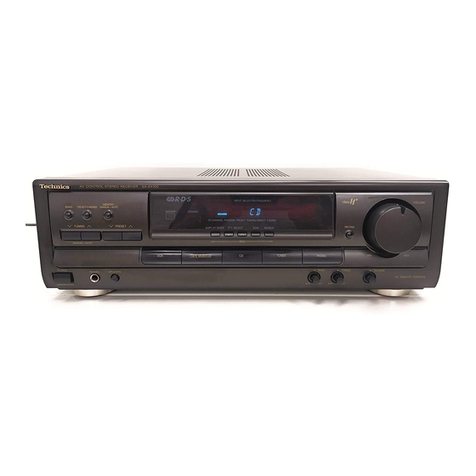
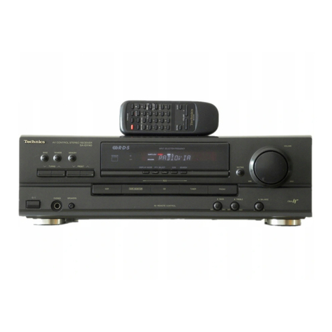
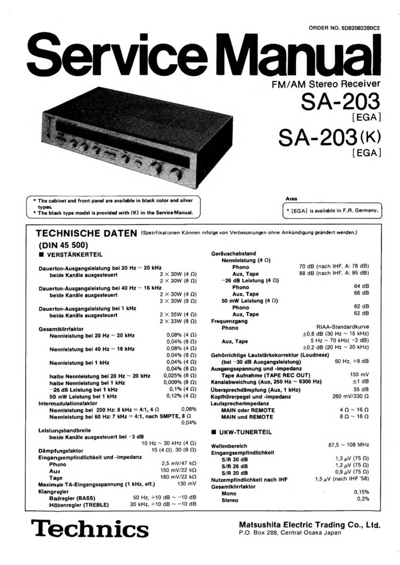
  9. Technics QUARTZ SA-160 User manual

Technics QUARTZ SA-160 User manual

ORDER
NO.
AD8807203C2
Service
Manual
CYUARTZ
Synthesizer
AM/FM
Stereo
Receiver
SPECIFICATIONS
(DIN
45
500)
@
AMPLIFIER
SECTION
DIN
power
output
1kHz
continuous
power
output
both
channels
driven
2x
40W
(8Q)
Total
harmonic
distortion
half
power
at
1kHz
0.07
%
(8Q)
Intermodulation
distortion
rated
power
at
60Hz:
7kHz=4:
1,
SMPTE,
8
0.5%
Power
bandwidth
both
channels
driven,
—3dB
10Hz~40kHz
(8Q)
Damping
factor
20
(89)
Input
sensitivity
and
impedance
PHONO
3mV/47kQ
CD,
VCR
1,
TAPE/VCR
2
200mV/22kQ
PHONO
maximum
input
voltage
(1kHz,
RMS)
150mV
SIN
rated
power
(80)
PHONO
68dB8
(IHF,
A:
71dB)
CD,
VCR
1,
TAPE/VCR
2
70d8
(IHF,
A:
85dB)
Frequency
response
PHONO
RIAA
standard
curve
+0.8dB
(30Hz~15kHz)
CD,
VCR
1,
TAPE/VCR
2
10Hz~70kHz
(+3dB)
5
band
graphic
equalizer
80Hz,
—-10dB~+10dB
250Hz,
—10dB~+10dB
1kHz,
—10dB~+10dB
4kHz,
~10dB~+10dB
Receiver
SA-160
Color
(K)...Black
Type
Area
Continental
Europe.
Holland.
Australia.
F.R.
Germany.
@
FM
TUNER
SECTION
Frequency
range
87.50~
108.00
MHz
Sensitivity
S/N
30dB
1.5uV
(75Q)
S/N
26dB
1.3uV
(75Q)
SIN
20dB
1.2uV
(75Q)
IHF
usable
sensitivity
1.5yV
(IHF
'58,
75Q)
IHF
46dB
stereo
quieting
sensitivity
22yuV/75Q0O
Total
harmonic
distortion
MONO
0.2%
STEREO
0.3%
SIN
MONO
60d8
(75dB,
IHF)
STEREO
58dB
(71dB,
IHF)
20Hz~15kHz,
+1dB~
—2dB
+400kHz,
65dB
Frequency
response
Alternate
channel
selectivity
Loudness
control
(volume
at
—30dB)
50Hz,
+9dB
Output
voltage
VCR
1,
TAPE/VCR
2
REC OUT
200mV
Channel
balance,
250
Hz~6,
300
Hz
+1dB
Channel
separation
55dB
:
Headphones
output
level
and
impedance
380
mV/330Q0
Load
impedance
MAIN
or
REMOTE
4Q~160
MAIN
and
REMOTE
8N~160
12.5kHz,
—-10dB~
+10dB
Technics
Capture
ratio
1.0dB
Image
rejection
at
98
MHz
40dB
IF
rejection
at
98
MHz
70dB
Spurious
response
rejection
at
98
MHz
70dB
AM
suppression
50dB
Stereo
separation
1kHz
40dB
10kHz
30dB
Carrier
leak
19kHz
—30dB
(—35dB,
IHF)
38kHz
—45dB
(—50dB,
IHF)
Channel
balance
(250
Hz~6,
300
Hz)
+1.5dB
Limiting
point
1.2uV
Bandwidth
IF
amplifier
180
kHz
FM
demodulator
1000
kHz
Antenna
terminals
75Q
(unbalanced)
Matsushita
Electric
Trading
Co.,
Ltd.
P.O.
Box
288,
Central
Osaka
Japan
SA-160
@
AM
TUNER
SECTION
Frequency
range
522~1611kHz
(9kHz-steps)
530~
1620
kHz
(10kHz-steps)
Power
supply
For
Australia
AC
50Hz/60Hz,
240V
For
continental
Europe
AC
50Hz/60Hz,
220V
Sensitivity
(S/N
20dB)
20uV,
330nV/m
Dimensions
(W
x
H
x
D)
430
x
97
x
288mm
Selectivity
at
999kHz
55dB
(16-15/16"
x
3-13/16”
x
11-3/16")
Image
rejection
at
999kHz
40dB
Weight
5.1kg
(11.2
Ib.)
IF
rejection
at
999kHz
55dB
Notes:
1.
Total
harmonic
distortion
is
measured
by
the
digital
spectrum
analyzer
(H.P.
3045
system).
M@
GENERAL
2.
Specifications
are
subject
to
change
without
notice.
Power
consumption
250W
Weight
and
dimensions
are
approximate.
i
CONTENTS
Page
Page
ACCESSORIES
|
cis
seseceocesscnssostancecsuouetcatscvnceraessssecsssiecssassorcescoseers
2
BLOCK
DIAGRAM
..........:cccccsesesesscrscessssceenrsereessecusenserneees
13~15
CONNECTIONS
TO
EQUIPMENT..........sc:cscsccssssesserssessessseenseese
3
DESCRIPTION
OF
FLUORESCENT
DISPLAY
............s0000005
16
FRONT
PANEL
CONTROLS
AND
FUNCTIONG.................
4,5
PRINTED
CIRCUIT
BOARDG.................
DISASSEMBLY
INSTRUCTIONG.............ccccssssessesseres
.
6~8
WIRING
CONNECTION
DIAGRAN
..
PROTECTION
CIRCUITRY
.........:ccccsscsssssssvsrsesessessessvseeersnesencoes
8
SCHEMATIC
DIAGRAM
............0..s0000e
BEFORE
REPAIR
AND
ADJUSTMENT
..........cccsssscsssssssseseesee
8
CABINET
PARTS
LOCATION
...........::ccsssessesecssusresenerneers
MEASUREMENTS
AND
ADJUSTMENTS......
9,
10
REPLACEMENT
PARTS
LIST..........cscsssssseseessesseserseresnes
FUNCTION
OF
TERMINAL
...........c0ccssssssssssssssesenecsesseeseee
11,
12
RESISTORS
&
CAPACITORS.
............csccsesssssssssessseresesesee
TERMINAL
GUIDE
OF
IC’S,
TRANSISTORS
AND
DIO
DE
Si
isc
ivncceccstcnn
ete
Rites
cadesdecevascaagulnedvandacdavanin
12
Mi
ACCESSORIES
©
FM
indoor
antenna
(1)
(SSA269M
[XL])
(SPB1161)
(SSA270M
[EX,
EH,
EG))
¢
AM
loop
antenna
(1)
*
AM
antenna
holders
(2)
(SMA233-1M)
(SMA231M)
‘ie
fan
(B)
*
AC
power
supply
cord
(1)
(SFDACO5E03
{EX,
EH)])
(SJA173
[XL])
¢
Screws
(2)
S
8
(XTN3
+
10AFZ)
Note:
Configuration
of
AC
power
supply
cord
and
FM
indoor
antenna
differs
according
to
area.
Mi
CONNECTIONS
TO
EQUIPMENT
“PHONO”
terminals
Connect
a
turntable.
Note:
For
remote-contro!
operation,
be
sure
to
“VCR
1”
terminals
Connect
a
video
cassette
recorder
or
an
audio
tape
deck
etc.
(Refer
to
the
operat-
ing
instructions
of
VCR,
etc.)
Video
cassette
recorder
(option)
connect
the
ground
wire
correctly.
Turntable
(option)
ae
ers
EES
2
(GND)
(R)
(L)
Ground
wire
(option)
Stereo
connection
cable
(option)
(GND)
(R)
(L)
iN
CD
REC
PLAY
REC
PLAY
OUT
BACK
OUT
Stereo
connection
Stereo
connection
cable
(option)
(R)
(UY
(A)
AUDIO
OUT
(O(ROR)
TT
“ORO
A)
cables
(option)
AC
power
supply
cord
(included)
The
configuration
of
the
AC
outlet
and
AC
power
supply
cord
differs
according
to
area.
Stereo
connection
cables
(option)
This
unit
Lolo
[ol
o|
P11]
2]
eIeS|eS|cs
a
(RL)
LINE
OUT
b
ie
Compact
disc
player
(option)
“CD”
terminals
Connect
a
compact
disc
player.
LINE
IN
Tape
deck
(option)
“TAPE/VCR
2”
terminals
Connect
a
tape
deck
or
second
VCR.
“SPEAKERS”
terminals
mw
Load
impedance:
MAIN
and
REMOTE
:
8~169
MAIN
or
REMOTE
:
4~160
LINE
OUT
m@
“REMOTE”
terminals
For
connection
to
a
second
pair
of
speakers.
®
Twist
the
core
of
the
speaker
wires.
2
@
Lift
up
the
lever,
and
insert
the
core
until
it
Can
no
longer
be
seen.
@
Press
down
the
lever,
and
pull
the
cord
gently
to
be
sure
that
it
is
secure.
@
10
mm
+
*T
(13/32")
=
Twist
ack
Notes:
1.
To
prevent
damage
to
circuitry,
never
short-circuit
positive
(+)
and
negative
(—)
speaker
terminals.
2.
Be
sure
to
only
connect
positive
(+)
cords
to
positive
(+)
terminals,
and
negative
(—)
cords
to
negative
(—)
terminals.
3.
Connections
of
speaker
wires
should
be
made
before
connecting
the
AC
power
supply
cords.
SA-160
@
FRONT
PANEL
CONTROLS
AND
FUNCTIONS
Amplifier
section
Audio
input
selector/frequency
display
(audio
input
selector/frequency)
[4]
7}
[8]
[memory]
s
___
stereo
(2)
pal
a
FM
fi
Lt
[|
Mrz
tuner
matrix
{loudness}
[quartz
lock
Tape
indicator
(TAPE)
Loudness
indicator
(loudness)
Power
switch
(power
)
Equalizer
controls
(graphic
equalizer)
These
controls
are
used
to
adjust
the
levels
within
each
frequency
band.
The
levels
can
be
varied
continuously
over
a
range
of
+10
dB~
—
10
GB.
By
sliding
the
controls
at
each
of
the
indicated
frequencies
in
the
‘‘+”
direction,
the
frequencies
in
that
band
are
boosted,
and
by
sliding
them
in
the
“—"'
direction,
the
frequencies
in
that
band
are
attenuated.
Loudness
switch
(loudness)
Set
to
the
“on”
position
(The
loudness
indicator
will
it
luminate.)
when
listening
to
music
at
low
volume.
Auditory
perception
of
sound
in
the
low
frequency
range
falls
off
at
low
volume
but
when
the
switch
is
in
this
position,
this
deficiency
is
compensated
for,
so
that
the
full
impact
of
the
musical
per-
formance
can
be
enjoyed.
Balance
control
(balance)
Voiume-control
(volume)
Headphones
jack
(phones)
Speaker
selectors
(speakers)
These
selectors
are
used
to
switch
the
speaker
systems
ON
and
OFF.
Input
selectors
(input
selector)
These
selectors
are
used
to
select
the
sound
source
Tape-monitor
switch
(monitor)
Press
this
button
to
listen
to
tape.
No
other
sources
selected
by
the
input
selector
can
be
heard
while
the
to
be
heard,
such
as
a
disc,
radio
broadcast,
etc.
tape
indicator
is
illuminated.
To
listen
to
some
other
source,
press
this
The
selected
sound
is
shown
on
the
audio
input
button
once
again.
selector/frequency
display.
Tuner
section
Signal-strength
indicators
(signal
strength)
These
indicators
show
the
relative
strength
of
broadcast
signals
being
received
by
the
antenna.
The
best
condition
for
reception,
for
FM
and
AM,
is
when
the
indicators
illuminate
completely
to
the
top.
FM
stereo
indicator
(stereo)
This
indicator
automatically
illuminates
when
an
FM
stereo
broadcast
is
being
received.
Note:
it
will
not
illuminate
if
the
FM
mode
selector
is
pressed.
Memory
indicator
(memory)
This
indicator
illuminates
when
the
memory
button
is
pressed.
Quartz-lock
5
[memory]
=
indicator
Preset
channel
RED
Aes
(quartz
lock)
matrix
display
rm
LILA,
This
indicator
(tuner
matrix)
tuner
matrix
quartz
lock
—
illuminates
when
tuned
precisely
to
an
FM
or
AM
station.
FM
mode
selector
(FM
mode)
Memory
button
(memory)
This
unit
automatically
switches
to
the
stereo
mode
This
button
is
used
when
preset
memory
setting
of
the
when
a
stereo
broadcast
is
received.
Press
this
preset-tuning
buttons
is
made.
selector
to
listen
in
the
monaural
mode.
The
stereo
indicator
will
not
illuminate
in
the
monaural
mode.
Preset
tuning
buttons
(1
~0)
(24
channel
random
preset
tuning)
These
buttons
are
used
to
preset
FM
and
AM
broadcast
frequen-
cies
into
the
memory
of
this
unit,
and
are
also
pressed
to
select
the
desired
preset
frequencies.
Note:
The
buttons
marked
[3)
~
[6]
are
also
used
to
listen
to
radio
broad-
casts
arranged
in
convenient
groups.
Group
select
button
(select)
Assort-mode
select
button
(assort)
Change-mode
select
button
(change)
Memory-scan/group-search
button
(-M.
scan/—group
search)
Character-input/tuning
buttons
(character/tuning)
RT
s
scmtinedaiepsiliaullonpelaniaseand
phones,
Band
selectors
(band
selector)
FM
-AM
input
satector
FM:
Press
this
button
'to
listen
to
an
FM
broadcast.
AM:
Press
this
button
to
listen
to
an
AM
broadcast.
allocation:
When
the
AMbutton
is
pressed
for
about
4
seconds,
the
AM
frequency
step
will
change
to
10
kHz
per
step.
(This
step
is
set
to
9
kHz
before
shipment.)
In
order
to
return
to
the
original
frequency
indication,
press
this
button
for
about
4
seconds
again.
SA-160
@
DISASSEMBLY
INSTRUCTIONS
“ATTENTION
SERVICER”
Some
chassis
components
may
have
sharp
edges.
Be
careful
when
disassembling
and
servicing.
Ref.
No.
Ref.
No.
How
to
remove
the
power
SW
P.C.B.
and
aaah
gcc
speakers
SW/headphones
P.C.B.
1
e
Remove
the
5
screws
(Q~@).
Procedure
1-2-3
¢
How
to
remove
the
power
SW
P.C.B.
1.
Remove
the
power
SW
knob.
2.
Remove
the
1
screw
(@).
3.
Release
the
tab.
¢
How
to
remove
the
speakers
SW/headphones
P.C.B.
1.
Remove
the
1
screw
(@).
Cabinet
Screwdriver
acto
How
to
remove
the
front
panel
Procedure
1-2
1.
Remove
the
4
screws
(@~®).
2.
Remove
the
flat
cable
(J501).
How
to
remove
the
FL
P.C.B.
Procedure
1-2-4
1.
Remove
the
3
screws
(@~®).
2.
Release
the
tab.
(No
1
side)
White
line
(2)
pul
/
push
|
Connector
SA-160
SA-160
Ref.No.
|
How
to
remove
the
tuner
P.C.B.
Ref.
No.
Ref.No.
|
How
toremove
the
volume
control
P.C.B.
|
Ref.
No.
;
and
main
P.C.B.
How
toremove
the
power
tc.
and
balance
control
P.C.B.
8
How
to
remove
the
key
switch
P.C.B.
Procedure
Procedure
Procedure
Procedure
1.
Remove
the
12
screws
(9~@®).
1.
Unsolder
the
power
IC.
¢
How
to
remove
the
volume
control
P.C.B.
1.
Remove
the
2
screws
(@,
@)
and
remove
the
2.
Remove
the
tuner
P.C.B.
and
main
P.C.B.
2.
Remove
the
2
screws
(@,
@).
1.
Remove
the
volume
control
knob.
P.C.B.
holder.
2.
Remove
the
nut.
2.
Remove
the
2
screws
(@,
©).
3.
Release
the
Tabs.
¢
How
to
remove
the
balance
control
P.C.B.
1.
Remove
the
balance
control
knob.
2.
Remove
the
2
screws
(@,
@).
Volume
control
P.C.B.
Unsolder
the
power
IC
Balance
control
holder
Note:
When
mounting
the
power
IC,
apply
silicon
terminal
compound
(SZZOL15)
to
the
rear
of
the
power
IC.
Balance
Volume
control
knob
control
knob
How
to
check
the
main
P.C.B.
1.
Remove
the
4
screws
(@~®)
in
above
figure.
2.
Remove
the
9
screws
(@~@).
3.
Remove
the
bottom
chassis
in
the
direction
of
the
arrow
(Q).
Mi
PROTECTION
CIRCUITRY
The
protection
circuitry
may
have
operated
if
either
of
the
following
conditions
is
noticed:
If
this
occurs,
follow
the
procedure
outlines
below:
1.
Turn
off
the
power.
¢
No
sound
is
heard
when
the
power
is
turned
on.
e
Sound
stops
during
a
performance.
The
function
of
this
circuitry
is
to
prevent
circuitry
damage
if,
for
example,
the
positive
and
negative
speaker
connection
wires
are
“shorted”,
or
if
speaker
systems
with
an
impedance
less
than
the
indicated
rated
impedance
of
the
amplifier
are
used.
2.
Determine
the
cause
of
the
problem
and
correct
it.
3.
Turn
on
the
power
once
again
after
one
minute.
Note:
When
the
protection
circuitry
functions,
the
unit
will
not
operate
unless
the
power
is
first
turned
off
and
then
on
again.
M@
BEFORE
REPAIR
AND
ADJUSTMENT
1.
Turn
off
the
power,
discharge
both
power
supply
2.
After
completion
of
repair,
slowly
apply
the
primary
capacitors
(C701,
C702
4700yF)
through
a
109
5W
voltage
by
using
a
variac
to
avoid
over
current.
resistor
to
ground.
Do
not
short
between
C701
and
Current
consumption
at
50Hz/60Hz
in
no
signal
C702.
It
may
damage
the
capacitors.
mode
should
by
shown
with
respect
to
supply
voltage
220V/240V.
Power
supply
voltage
Bottom
chassis
50/60
Hz
120~320mA
|
100~300mA
Mi
MEASUREMENTS
AND
ADJUSTMENTS
mFM
Control
positions
and
equipment
used
¢
FM
signal
generator
(FM-SG).
Stereo
modulator
*
Distortion
analyser
¢
Oscilloscope
eAC
and
DC
electronic
voitmeter
(EVM)
e
Frequency
counter
¢Choke
coil
(100yH)
¢
Resistor
(100
kQ)
Note:
For
2201,
Z202,
L321,
L322
and
L324,
adjusted
parts
are
supplied.
So,
do
not
turn
the
cores
of
these
parts.
FM
MONO
DISTORTION
ADJUSTMENT
1.
Test
equipment
connection
is
shown
in
figure.
2.
Set
the
unit
to
“FM”
position.
3.
Set
the
radio
frequency
display
and
signal
generator
to
100.10
MHz.
4.
Adjust
T201
core
so
that
voltage
measured
in
signal
mode
is
OmV
(0+20mV)
in
300mV
range.
}.
Adjust
T202
so
that
the
distortion
factor
of
Lch
is
minimized.
.
Repeat
steps
4
and
5
a
few
times.
.
Make
sure
that
the
distortion
factors
of
Lch
and
Rch
are
nearly
the
same
with
each
other
to
minimum.
Note:
The
adjusting
screwdriver
used
should
be
made
of
resin.
MPX
VCO
ADJUSTMENT
.
Test
equipment
connection
is
shown
in
figure.
.
Set
the
unit
to
“FM
auto”
position.
.
Set
the
radio
frequency
display
and
signal
generator
to
100.10MHz.
.
Adjust
VR301
for
19.00
+0.03kHz
on
frequency
counter
reading.
%
USING
ALTERNATE
SYSTEM
1.
Apply
stereo
signa!
from
generator
or
receive
the
stereo
broadcast.
‘2.
Adjust
VR301
until
stereo
indicator
lights
up.
Cement
arm
of
VR301
as
shown
in
figure.
FM
STEREO
SEPARATION
ADJUSTMENT
(For
[EG]
area.)
1.Test
equipment
connection
is
shown
in
figure.
2.Set
the
unit
to
"FM”
mode.
3.Set
the
radio
frequency
display
and
signal
generator
to
100.10MHz.
4.Adjust
VR302
so
that
the
R-CH
output
is
minimized
when
stereo
modulator
is
in
“L”(L-CH
modulation)
mode.
FM
SIGNAL
GENERATOR
CONDITION
Modulation
Modulation
frequency
1kHz
(MONO)
Output
level
FM
SIGNAL
GENERATOR
CONDITION
Modulation
0%
FREQUENCY
FM
ANTENNA
COUNTER
TERMINAL
:
Stereo
ON
position
®-
©)
-
©):
Stereo
OFF
position
-@
{indicator
lighting)
©
:
Adjust
point
of
Pilot
circuit
FM
SIGNAL
GENERATOR
CONDITION
Modulation
Stereo
“L”
mode
or
“R”
mode
‘90%,
Pilot
10%
Modulation
frequency
1kHz
(Pilot
19kHz)
Output
level
LPF
(fo=
T5kHz~
19kHz)
SA-160
FM
STEREO
DISTORTION
ADJUSTMENT
(For
[EG]
area.)
FM
SIGNAL
GENERATOR
CONDITION
Modulation
Stereo
“L’’
mode
or
“R”
mode
100%
1.
Test
equipment
connection
is
shown
in
figure.
2.
Set
the
unit
to
“FM”
mode.
3.Set
the
radio
frequency
display
and
signal
generator
to
100.10
MHz.
4.
Adjust
L1so
that
the
distortion
factor
of
L-CH
is
minimized.
5.
Make
sure
that
the
distortion
factors
of
L-CH
and
R-CH
are
nearly
the
same
with
each
other
to
minimum.
Modulation
frequency
Output
level
Notes:
1.
The
adjusting
screwdriver
used
should
be
made
of
resin.
2.L1
should
be
rotated
no
more
1/4
turn
(90
deg.)
on
either
side.
Stereo
modulator
Adjust
within
+90°
Output
mode...
Lor
R
e
Adjustment
points
AM
ANT
FM
ANT
FM
offset
coil
FM
MONO
DISTORTION
coil
FM
STEREO
SEPARATION
Adj.
MPX
VCO
Adj.
SA-160
SA-160
Mi
FUNCTION
OF
TERMINAL
e
10901
(LC6554H3682):
microcomputer
DESCRIPTION
OF
TERMINAL
Segment
signal
output
Key
return
signal
input
—
-}
STAND
BY
Power
supply
terminal
OFF
Power
ON/OFF
input
1
STEREO
Stereo
signal
input
SD
signal
input
=
No
>=
20-2
N
a
NO
°o
EE
ae
ae
<
1/0
Deck
control
terminal
=a]
(oe)
4
RELAY
Relay
control
output
:
N
Not
connected
Auto/mono
changeover
terminal
—
fo]
Muting
control
output
Attenuator
control
output
AFM
AF
signal
muting
control
output
=
ie}
Ground
terminal
vU
Vss
Ground
terminal
24
OSC1
Oscillator
terminal
OSC2
Oscillator
terminal
nD
Reset
signal
input
PFO/D1
Serial
data
output
terminal
27
PF1/CK
Clock
signal
terminal
for
serial
data
PF2/CE
Chip
enable
terminal
PF3/INT
Remote
control
input
30
Ground
terminal
[e%)
prs
le
32
Cc
Ground
terminal
n +
Control
signal
terminal
for
|C401
(TC9163N)
wo
i?)
DESCRIPTION
OF
TERMINAL
Not
connected
hy
gees
|
LOUDNESS
ro.
Loudness
control
output
PJO
(R)
PJ1
(F)
iy
ae
Ne
We
ie
Power
supply
terminal
(negative
voltage)
44
$2
J
$12
Volume
motor
drive
output
Segment
signal
output
LC6554H3682
(64
PIN)
28J40CD
2SK381
SVGLB74UR3HL
~~
2802785,
2SC2787,
2SD1450
ES
c
B
[um7oot
_[@
PIN
AN72796
[16
PIN
swrorncs|
16
Pin
|
TooT6aN
[26
PIN
Cathode
SVDS2V20,
188133,
|
_
MA29WA,
MA167,
SVD1SR35200A
Anode
28B1185,
28D1762
Anode
MTZ6R8B,
MA4056M,
MA4110M,
MTZ15BT77,
Cuiaee
MA4030M,
MA4062M,
,
MTZ30BT77
Cathode
Ca
o——_}<}0
A
AA1A4M,
AA1A4Z
e-
aGr)
E'
Mi
BLOCK
DIAGRAM
FM
MONO
DISTORTION
adj
R313,
C33
Q301~Q303
MUTING
TP201°TP20I*
202
FM
ANT.
fl
£T°y
FM
FM
FRONT
END
aE
i
ec
Coil
CB)
—-
me
eee
eee eee
ee
ee
ee
ee
cr20}
cr202
7
df
ais
AZ
7
es
a
ne
ee
RF
Amp
FM
IF
i
arc]
wet
Veo
Ic2ol
}
AM/FM
IF
1
I
—_]
=
i
|
1C201
|
0
rs
MIX.
4,
4
—_]
——_]
FM/AM
FM
IF
|
FM
oer.
Muting
]
&
I
$
!
9201,a202
74
IF
Level
Det.
I
|
2202
|
|
:
pe
|
[=
|
"
cd
3
|
>
Pfr
¢
L_
poeta
os
ed
|
Meter
|
WY
FM:
ON
H
=
=
a
“8
;
alka
:
ae
os
Q208,
AM
IFT
ri
;
|
aio2
FM
_LOOP
l
scat
|
Kexteh]
|
EM/am
FORCIBLE
6
FILTER
|
cS
?
Lm
|
Power
supply
HB)
|
[|
MONO/
A
5
AM
AM
AM
|
Selector.
|
vco
STOP
RF
MIX.
OSC.
age
Der.
|
!
|
|
2
19KHz
<
|_figKHz
=
LAMP.
i]
Ge
I
1166
S40
HEHE
eB)
Ge
!
we
OF
—
Om
ee
ee
Oe
ee
Om
ome
me
Oe
ome
1
2
5
2201
on
hae
.
mM
ake
1
Eee
|
Mi
G8)
I
bee
dh
ee
ea
ee
ee
AM
ANT.
COIL
AM
i
Is
9
’
AM
OSC.
COIL
T
+H
Ic30l
_
FM
MPX
AE
VR301
TP301
O—
J
MPX.
vco
adj.
MPX.
VOO
adj.
—
a205,
AM
Q206
CS
bs
>
Ic
10]
K
PLL
FREQUENCY
Cea)
SYNTHESIZER
i
|
POWER
TRANSFORMER
$701
Fl
i
1
AC
IN
!
1
1
CE
CL__
DATA
3
4
5
28
29
ay
ce
19
!
12
!
Q701,703,704
Q705,707
REGULATOR
REGULATOR
D70IND704
RECTIFIER
9708,
Q709
REGULATOR
Q710
REGULATOR
CF901
To
FL
co
}
5
(4MHz)
|
25
;
osc2
|
REMOTE
she
CONTROL
&
RES
TAPE
TERMINAL
Qgoi
OFF
RELAY
si2
—
——
—
|
|
|
{
I
|
!
I
{
|
aal
of
8
®
18
Ly
138.
20
Voo
AT
7
st
MONO
STEREO
rc
oe
we
oe
oe oe
oe
=
MICROCOMPUTER
¢®
From
POWER
{
FL
DISPLAY
TRANSFOMER
KEY
MATRIX
EQUALIZER
AMP
r
'
'
A
dey
’
ant
He
PSA
cost
“
&
sol,
\
PHONO
'e
!
(3)
1
1
1
Os
—
==
'
a
©
Ar
see
(26)
;
S2
!
f
bm
0
\
\
¢
4
aex
weil
1,
$3
'
°§
=|
eal
{
re
1
{oietee
aaa.
|
(23)
+
54
1
fe
REC
OUT
we
i
'
TAPI
i
E
]
pane
be
L
2a!
,
85
1
PLAYBACK
(QX-—»>—
a
5
,
J
|
1
al
Fecal
re
(20)
1
REC OUT
SS
er
5
1
i
12
1
:
I
vcR
|
10
+
t
~
I
L
PLAYBACK
SS
ee
8)
VCR2
AUDIO
IN
g
~
|
[ise
or
4
icoceeme
circuit
rt
[
snift
regist
|
regist
O
TORTION
adj
Ic20l
AM/FM
IF
FM/AM
!
!
Power
supply
+B)
|
I
selector
SCHMITT
5s
5
RCUIT
mz
mi
FORCIBLE
I.
MONO/
4
r
z=
LAMP
:
rl
FF.
DRIVE
CO
STOP
—
=
|
-
10
15
FM
AM
H
I
lee
Sete
oe
SS
Ses
Sd)
14
15
J
IC301
Q301~Q303
MUTING
R ch
GE(B.P.F.)
oe:
a
|
1
1C551
|
10451
eo
&
|
l
EQUALIZER
AMP
28
ul
I
CTT
or
=]
C401
748.
v
3
cr
ne
a
St
Pe
}
SELECTOR
|
|
ete
arenes
|
]
’
ent
+.
3!
i
!
|
!
°
5
’
$l,
'
|
HONO
(©
gb
\
¢
(3)
1 1
H
|
aes
:
!
CB)
8)
1
ee
ay
!
"4
2!
j
S2
!
i]
aa
ee
©
|
al
gee
fi!
I
(25)
$3
'
cD
Qu
—$—9-~o
1
]
5|
\
i
(24)
4
1
4
I
Cath!
(23)
,
34
I
|
Cs)
@)
REC
OUT
(©
ae
\
|
fe
1
1
Af
oe
TAPE
!
[
‘|
uae
—¢
To
af
ery
‘|
(22)
!
(20
(5)
]
PLAYBACK
g
>
1g
55
}
‘
7)
U
Oo
!
ap
24
e>
0501,0513,a514
!
REC OUT
|
!
B
LOUDNESS
[
\
!
CONTROL
!
|
vcr
I
+
1
I
i)
2
PLAYBACK
e-
;
vcr2
AUDIO
IN
g
~
Ay
vR301
TP301
©
FM
MPX
7
MPX.
VCO
adj.
MPX.
VCO
adj.
Q205
a206
2
SIGNAL
DET.
oe
—-
c
b
a
33.
18
1
56
20
—
ST
MONO
STEREO
Yoo
za
AT
“7
~
O
cK
Bz
a
DI
KEY
08
r a
12
re
1C901
MICROCOMPUTER
a
D
nn
=
a
ree
g
LOUDNESS
44
CF901
(4MHz)
—
i]
25
osc2
|
REMOTE
26
CONTROL
SReS
TAPE
TERMINAL
@)
Qsol
OFF
RELAY
of
On
ee
ee
ee
ee
ee
RESET
10
14
aay
Zl
K
a)
From
POWER
{
FL
DISPLAY
TRANSFOMER
MATRIX
POWER
AMP
ila
rom
ee
(4)
1
y,
E
4a
8
VRS5OI-
1
Coe
Oe
my
VOLUME
3|
Hee
|
¢
aA
[:
I
(7)
&
2
(6190
J
VR5O1-2
=
©,
BALANCE
IC501
503
BUFFER
MUTING
SWITCH
Rech
Q505,
Q506
MUTING
CONTROL
iS
0
HEADPHONES
s6ol-2
(REMOTE)
ON
0
£
cote
REMOTE
7
Qo
—
SPEAKERS
on
O
4B
al
|
MAIN
oO.
‘
!
i)
t
S60I-1
|
(MAIN)
I
>
Note:
¢
===
FM
Signal
¢
coon
FM
OSC
©
ae
AM
Signal
°¢
suse
AM
OSC
SA-160
li
DESCRIPTION
OF
FLUORESCENT
DISPLAY
M@
PRINTED
CIRCUIT
BOARDS
¢
Grid
assignment
(PLAY
BACK)
VCR
f-_TAPE/VCR2},
(REC OUT)
[eo]
PHONO
(REC
OUT)
(PLAYBACK)
k
quartz
loc
IX
tuner
||
matr
c
MAIN
(PHONO
EQUALIZER
/
INPUT
SELECTOR
/
POWER
AMP/
POWER
SOURCE
)
PC.B.
3G
the
EG(F.R.Germany
)area.
In
Resistors,
Capacitors
and
Coils
indicated
by(C),(R)
or(L)
are
used
only
i}
bile
2
t
a(R)
answered)
e
Pin
connection
ricoei
e
Anode
connection
in
See
Ge
ff
-
me
bore
ee
2
ee
2
M@
PRINTED
CIRCUIT
BOARDS
w
fo
WwW
xg
do
Wu
oo
ao
=
r-LVCR
(REC
OUT)
TAPE/VCR2
(REC OUT)
oa
[co]
PHONO
[6no|
T701
POWER
TRANSFORMER
ad
EE
so
88
©
FR
——m
be
Fi
$3
2]
-LN
g
=|
298
Oo!
SO:
ec3-
he
aa
Olss6
wo
zt
om)
oe
un
|
we
2¢
cues
=x
i.
ia
x
Sears
|
ee
o 0
-
rere
POWER
SOURCE
PC.B.
oa
rt
oR
ee
{R)
or(L)
B
PC
indicated
by(C)
.R.
Germany
)area.
tors
and
Coils
Ww
oO
Ww
©
£
=
os
a>
oc
Lox-)
o]
©
n
3
©
2
i]
Resistors,
MAIN
(PHONO
EQUALIZER/
INPUT
SELECTOR
/
POWER
AMP/
POWER
SOURCE
)
(PLAY
BACK)
.
ed
(PLAYBACK)
For
(EG)
area.
r
oe
&
Gono
4
|
|
|
|
|
|
|
|
|
|
|
Aj
{AC220V
50/60Hz)
a
ol
Z
&
8
For
‘
SOURCE]
POWER
TRANSFORMER
T7Ol
POWER
PC.B.
AC
IN
(220V
or
240V
50/60Hz)
For(EX,
EH,
XLJareas.
i
POWER
SWITCH
PC.B.
©
©®
LJ
POWER
\—orG
ie
es
Hi
WIRING
C
(o)
N
;
a
oO
a
wo
Sy
O
=
59
a
2
=”
WwW
2
wm
Wi
a)
%
zi.
3
fos
&
Wris
(0)
é
<a
|3
wis
|S
24
OX
r
a
0
oO
=
a:
xr
iO
Se
os
an
a)
-
a
a
a
2
he
2
ow
g
%
©
-
x
oO
a
a
NO
Za
o2a
no
-a@
zo
A,
its)
af
-
:
a
ro
a
a
=
<q
a
Nw
wi
24
q
aD
Go
“|
Go
ie
=o
aT
Lo
lo]
4
Lu]
°
be
|
- —
uw
n
w
&
=
=
8
8
o
aoe
z
_
Z
=
x
al
gl
&
:
N|
&
2
pay
4
aq
=z
ihe
°
Oo}
x
Wy
x
tv
=
N
:
i
=.
o
3
a|
=
oO}
gs
F
a
=
oO
N
a
:
N
cy
a
x
.s)
E
=
a
z
9°
|
sd
<q
na
Pe
ao
ro)
=<
I
Las
LL
|
WERT)
$24
(TUNER)
ES
ad
(MAIN)
(REMOTE)
SPEAKERS
a/
=
PHONES
POWER
INPUT
SELECTOR
ones
[LOUDNESS
|
RT]
[SELECT]
[
MEMORY]
[CHANGE]
[asso
CHARACTOR/
TUNING
[FM
MoDE]
[BAND
SELECTOR|
BALANCE
VR.
PCB
|9kHz
output
TUNER
(FM/AM)
PC.B.
=
EG,EH
E
W
1S}
2
¢
a
o4
a
VOLUME
PC.B.
1
LWysz-—raNo)
'
4iNv
doo7
<1!
(US2)
WV]
|LNV
WV
S
LNV
W4
ire
L203
For(XL]
area.
VOLUME
FM
off
set
voltage
(0
mV)
AMP
PC.B.
LED
PCB.
(Signal
strength
ind.)
SPEAKER
SWITCH/
HEADPHONES
JACK
PC.B.
For
(EG
Jarea.
POWER
[MONITOR
]
SWITCH
PC.B.
S27
326
?
(TRPE/VcR2)
(VERT)
$24
325
Boone)
ATUNER)
SHON
(REMOTE)
(MAIN)
SPEAKERS
PHONES
19
kHz
output
C
BALANCE
VR.
PC.B
[BALANCE
O
mV)
Mi
WIRING
CONNECTION
DIAGRAM
For(EX,
EH
,XLJareas.
For
(EG)
area
AC
IN
AC_IN
(AC
220V
50/60Hz)
(220V
or
240V
50/60Hz)
SPEAKER
IMPEDANCE
SPEAKERS
s702
=
gE
POWER
T70!|
TRANSFORMER
BLU
BRN
J
POWER
SOURCE
PC.B.
y6OI
FL
METER
DRIVE/
(LIL
LL
LLL
LILI
I
III
ITLL
IIIA
LLLP
LT
IIIS
ISIS
SSDS
LSD
DID
LLLP
riveRi}
—
[rapervcr2]
[co]
[PHONO]
[6no
(REC OUT)
(REC
OUT)
(PLAYBACK
)
A
(
PLAYBACK)
om
[iN
i
MAIN
(PHONO
EQUALIZER/INPUT
SELECTOR/POWER
AMP/POWER
SOURCE)PC.B.
v501
GRAPHIC
EQUALIZER
AMP
P.C.B.
[exon
——S
J906
y907
y901
y902
J903
(234567)
(23456)
g
ang
POWER
SWITCH
PC.B.
—
BRN
Horst)
©
SPEAKERS
s70l
PoweR
LH
|
SPEAKER
SWITCH/
HEADPHONES
JACK
P.C.B.
si4
sie
||
si7
[se
][si9
sz]
906
907.
s3]
ss]
[se
Ss
$8
se]
[si
su
J905
[234567]
LED
PC.B.
BALANCE
VR.PC.B.
BALANCE
$27
S26
J20l
J202
VOLUME
SA-160
Mi
SCHEMATIC
DIAGRAM
(This
schematic
diagram
may
be
modified
at
any
time
with
the
development
of
new
technology)
Note
1:
°$1~S10
:
Preset
tuning
switches.
$1:
1,
$2:
2,
S3:
3,
$4:
4,
S5:
5,
|
ea
6,
S7:
7,
$8:
8,
S9:
9,
S10:
0
°Si1
:
Memory-scan/group-search
switch.
©
$12
:
FM
mode
select
switch.
(AUTO++MONO)
°
$13,
$14
:
Band
selectors.
$13:
FM,
S14:
AM
¢
S16,
S17
:
Character-input/tuning
switches.
$16:
down,
S17:
up
°
$18
:
Change-mode
selector.
©
$19
:
Assort-mode
selector.
¢
$20
:
Group
select
switch.
°
$21
:
Memory
switch.
¢
$22
:
Loudness
switch.
¢
$23~S27
:
Input
selector
switches.
bios
phono,
S24:
tuner,
S25:
CD,
|
$26:
VCR1,
S27:
tape/VCR2
¢
$601-1,
S601-2
:
Speaker
selectors.
$601-1:
main,
S601-2:
remote
e¢
$701
:
Power
switch
in
‘‘on”
position.
®
Signal
line
ema
:
B.P.F.
signal
<——>»
:
FM
signal
coon
:
FM
OSC
aaa
©
AM
signal
auaap
:
AM
OSC
:
AF
signal
(Lch)
crzzzrfp
:
Phono
signal
—<
>—
:
Positive
voltage
lines
--<
>--
:
Negative
voltage
lines
¢
Important
safety
notice:
Components
identified
by
A
mark
have
special
characteristics
important
for
safety.
When
replacing
any
of
these
components,
use
only
manufacturer's
specified
parts.
Indicated
voltage
values
are
standard
values
for
the
unit
measured
by
the
DC
electronic
circuit
tester
(high-
impedance)
with
the
chassis
taken
as
standard.
Therefore,
there
may
exist
some
errors
in
the
voltage
values,
depending
on
internal
impedance
of
the
DC
circuit
tester.
¢
All
voltage
values
shown
in
circuitry
are
DC
voltage
in
FM
signal
(Stereo
signal)
reception
mode.
*
Figures
in
(
)
Stand
for
DC-voltage
in
AM
signal
reception
mode
*
Caution!
IC
and
LSI
are
sensitive
to
static
electricity.
Secondary
trouble
can
be
prevented
by
taking
care
during
repair.
*
Cover
the
parts
boxes
made
of
plastics
with
alminum
foil.
*
Ground
the
soldering
iron.
*
Put
a
conductive
mat
on
the
work
table.
*
Do
not
touch
the
legs
of IC
or
LS!
with
the
fingers
directly.
Note2:
°
Use
of
ceramic
filters
in
pairs
The
ceramic
filters
(CF201,
CF202)
for
FM-IF
circuit
are
available
in
three
ranks.
For
this
circuit,
be
sure
to
use
the
ceramics
of
the
same
rank
in
a
pair.
At
repairing
and
replacement,
pay
close
attention
to
the
diodes
(D914,
D915)
for
use
as
different
diodes
must
be
used
depending
on
each
rank
of
the
ceramic
filters.
CENTER
FREQUENCY
se
10.65
MHz
10.70
MHz
ox
x
10.75MHz
Note:
©
mark:
Diode
is
used.
x
mark:
Diode
is
not
used.
->—
‘For
(XL)
area.
[em
ANT
(759)
For
FM
ANT
AM
ANT.
-AM
|
LOOP
ANT
GND
tLech
PHONO
Rech
[Lch]
cD
[-REC
OUT
VCRI
UPLAYBACK
r-REC
OUT
TAPE/VCR
2
PLAY
BACK
[Ra]
60
[-REC
OUT
VCRI
LPLAYBACK
[REC
OUT
TAPE/VCR2
“PLAYBACK
(EX,EH)
areas.
YQ)
%
|
2
aap
as
a
1)
(759)
seg
iP
ae
a
:
re
©)
YQ
(Oj
Y
i
Cc
OF
SA-160
SA-160
3
4
6
For
(EX
;
EH,
XL)
areas.
For
XEN
XL)
areas.
-----
820K
For
(EG)
areo.
470K
TNIO!
(FM
FRONT-END
PACK)
SNVFE203E01
ee
a
eae
ee
Ak
had
lh
en
re
a
a
ee
a
(c20l
__FM
signal
+
$c2668
|
AN7273A
2SK439
-
Cece
!
-
FM/AM
IF
AMP,
—
rene
—t-)
|
ae
C)
Bi
Sc?
DET®
AM
MIXER,
l
7
f
S
|
&
Cees
|
28¢2787
sie,
i
|
FM
IF
AMP
jicior
2
;
6
“Y2-~LM7001
Jpb—--—----——==
1
1
1
:
PLL
FREQUENCY
H
SYNTHESIZER
1
114.6V
(Cv)
c208
6V100
b
2s
1F
L
For
others.
Tpas7
|
l
peo
|
i
CL
DATA
Syc-
Bor
---@--@)-----@------
180K
~680K|
0.02
7K
2SC609
FM
OSC
signal!
4
2Sc2995
is
J
FM AM
Pd2
PD!
Voo2
Vool
=
AMOSC
0S
|
vy
6226
20.01
sav
eS
‘area.
i
R216
56K
Foreele
fas
Goel
Sy
ar
ae
Q208
oy
9207
{
a
5vill45y,,
:
me
|“
Pane
ss
;
at
Ch
¥
Sys
aa
Vv
4
<.6V
~ 2
MA4IIOM
2SCB28A
aa,
AM
OSC
BUFFER
2
Q208,209
:
2SA564A
25C8785
23V
aN
POWER
SUPPLY
(
FM/MW/LW)
2
EQ
tuneriFm/am)
circuit
Pram
LOOP
Uv}
FILTER
-530kH2
=—=1620kH2
c4I7
0.01
a
C463
R457
C457
C459
6V33
270
0.022
0.0068
Phono
signal
BUFFER
AMP
CIRCUIT
cae
Poel
R507
C50:
:
E}
Hi
8.2K
I6VIO
00!
2,
6
ex
l
oo
0.
R461
R463
180K
12K
—ehy
-15.2V
C5I7
0.01
1c501
AN6552F
BS
3
BUFFER
AMP
re
2
oa
o
R68!
58
2
1K
Ls?
&
<£8)15.1V
es06
5
‘oO
=
:
R673
=
BS
C464
Re
8
rr
=
ee;
‘a
ae
B58
-£460,
g
For
(EGJarea.
R508
C510
no
o
3S
R401
3.3K
en
as
R5IT
56K
|
itn
Qs506
Q505
AAIA4MTA
ANIA4
MUTING
CONT.
MUTING
acvead
698
R421
3.3K
C407
Q505
Qs06
15.1v
Grd
10K
A
1c401
TC9IG3N
IN
PUT
SELECTOR
Se
For
(EG)
area.
C419
6VIOO
oP
ae
is
C4
Hi
C416
0.01
mi
INPUT
SELECTOR
CIRCUIT
2
3
4
5
6
7
8 9
10
11
12
.
1c
301
Sait
=
For
(EX,EH,XL)
22K
For
(EX,
£H,XL)
areas.
Fee
eed
ete
econ
a
S20
AN7470
"i"
BS
ge
tee}
erage
2
a
ee
es
ee
FM
MPX
27)
&
TNIO1
(FM
FRONT-END
PACK)
SNVFE203E0I
/
c206
ISP
L321
‘For
(XL)
area.
FM
signal
(ooo
rr
rr
rn
rr
nena
nn
a
enone
se
-e
7
2
2o
ee
cbt
oe
Bee
Py:
=
For
(EG)area.
2SK439
par
a
2SC2668
“
ge
/
gS
R204
&"
cr202
aN
Seen
c-
ar
(esiate
38
For
(EX,EH,
Sx
R313
C305
FM
ANT
i
EN
RF
AMP
FM
MIXER
|
Sms
Oo
R202
Sook
Le
a
as
N
u
XLJareas.
|&*
RR
SONS
S
fa
A
5.
“a
a2
|
83
°
—
DET@
AMMIXER
.
BV
eesenanenmmmncnccnannant
iP
O—
=>)
eS)
|
=>
|
orzo
ef
evi
LI|LL}
20,202
its
“
i
a.
@)
aN
Deere)
) )
\caica!
so
2sc2787
€313'0.001
$c306
‘
18
E
J
0
YJ
Us
6204
AK
i
i
FM
1F
AMP
1
R314
47K
}50v33
L322
)1(75Q)
@)
A
!
iSs|oj
ow
47P
ane
jicior
>
|
R30
sare
nyy
44_f
'
ao
625
b
hi
i
:
\
6
Wh
5
'
H
201
a202
2
~LM700
|!
HOU
tiers
are
'
J
!
Si
none
parmaeee
be
oe
GND
&Y
|
"
|
<
H
2
-
5.
BV
7
a
1
|
186v
28
(10.7v)I10.7V)
|
(5.8V)
£
58V)
he
:
Cae!
paras
SI
83
7v
le.i1v
liosv
losv
sev
g5.6v
Lov
3e
For
@)
sist
so
av)
O—-O--©—-O—-®
=
E
(EX,
EH)
areas.
oT
6
i
|
]rse
ati
Pe
heal
2B
g
ee
oe
Net
g
Pe
|
cee
eon
B8L
|e
pie
rik
|
scor]
23
8
g
Far
oters
oe,
3
eee
pects
i}
|
Be
sal
Tt
1
Oo
'
o
q
nae
one:
=O.
\alte
|
a
fed
=
!
|
2P
O
tas
f
z
(-)
zsceoo
|
ol
i|
¥
ss
AM
A
é
ae
=
\
[
L328
]
'
$3
OTs
signal
L
28c2995
ria
enero
ee
ay
°°
|
981
8x
AM
ANT
Q
1
1
|
For
€GJarea.
6
FM
offset
(ei¥0
eol®
Jbe-~--------------------
-------------------
M
:
‘ .
0
0
vo
tage
(Omv)
MGZXE
¥
7
oo
203
-
;
its
I9kHz
output
Be
i?)
ip
AM
ANT
coil
AM
OSC
coil
x
|
|MPX
VCO
adj.
[es
tA)
sic
o
|
igeences)
eeeel
ores
eet
:
LOOP
ANT
3
"9301,
302
Q301
2SD
1450
MUTING
tO}
208
oy
0207
, i
&
.
:
(14.5v)l4.5
(l
-
>
et
p
CY
Koay
R2!5
82k
[
pz0g
wales
i
:
6av
==222--}4--=-4--2222-
18
e
IW
fo2!
$80
ming
©)
es
:
: :
9208
ee
R227
100K
AI65
a
=
q
Q303
28CB28A
9g
|
2
2SA564A
AM
OSC
BUFFER
-
SUPPLY
Q206
os
S7SMi=
=
Genz
0208,209
(FM/MW/
2SA564A
MUTING
CONTROL
V
(aM)
UK,
2SA564A
SIGNAL
DET.
Q10!
102
zayf
BS
POWER
SUPPLY
(
FM/MW/LW)|
2SC2785
A
AY
TUNER
(FM/AM)
CIRCUIT
FM/AM
LOOP
Lavi“
|
FILTER
-S30kH2
==
1630kH
C4I7
0.01
.
eno
OQ
Phono
signal
SS3
B47
82
SR
B
MAIN
CIRCUIT
BUFFER
AMP
CIRCUIT
R671
470
oO.
a
R459
c46i R467
Q503,
504
rLch©
=
ao
ep
oe
88
68
25V3.3—
IK
2SK381
R507
cs09
vane
|
821
rere
LS
2533
bo
5
MUTING
AWE
505
RchO
253.3
~
15.1V
gens
EK
DEVE
BTENSEO
|
gemrmmmmmnmnnnnennns
jones
-
4
(5)
37
ov
fov
fisav
<|
28
5
cD
©
DS
ANGSS2F
i
8
Ic5Ol
Se
Ee
ae
es
ae
oe]
AN6552F
Geni
Revs
8S
#3
87
=
4)—@)—2)—C)
iy
8
SEER
AME
:
tk
S82
a
on
i
PHONO
EQ
AMP
CIRCUIT
“PLayBack
©
say
°
hase
Eszv[ov_Jov
Tov
Cis2v
©—O-
§
agel
SS
:
3
ov
yov
&
TREC
out
Gr
VK
sete
d
452
ge
fRASO
R42
Race
ae
R468
387
6K
5]'5-'V
csog
Fs
:
R673
=-8S
casa
nase
|
8
2
tx
al
2
+H
OE
eaee
om
1K
Te
‘
=
C458
|
C460
¢
For
(EGJarea.
es
8
2
R508
C510
3
Ts
4
R401
3.3K
aa
F
r
R5I7
56K
co
:
ext
Tiles
|
23
aioe
aos
REa4
zo
eleoye
88
AAIA4MTA
ANIA4SMTA
¢
ab
REC
OUT
G
=
d
cee
|
MUTING
CONT.
MUTING
CONT.
vor!
R676
LY
PLAYBACK
©
=
R421
3.3K
o
reaz
LS
cat
/VCR2
‘ere
TSB
arya
a
i
tenes
FFL
paos
Q506
15.1v
/70K
per
—
PLAYBACK
e
+
mM
=
3
‘
Sa
ak)
\
Ee
=|
1c4o1
#
=
wee
aed
One
as)
E
TC9I63N
WE
sem
IN
PUT
1c402
For
(EG)
area.
SELECTOR
AN6S52F
C419
6vi00
BUFFER
+
AMP
d
rs
ie
c
zs
b
a
:
2s
Liss
za
5
oy
,
BS
88
b
ia
Q513,514
sos
2
For
(EG)
area.
=
a
S
AAIA4MTA
zoe
=
ewes
d
K15.2v
<6|-Is2v
=
MUTING
c
26
2
CONTROL
se]
s[
INPUT
SELECTOR
CIRCUIT
—
3
—
—
24
—
13
14
15 16
17
18
19
20
21
22
FL9O!
SAD8MT38GK
SYSTEM
CONTROL/FL
DRIVE
CIRCUIT
GRAPHIC
EQUALIZER
AMP
CIRCUIT
c580
R554
---4V
FL
METER
DRIVE/
r—
iz
FL
DISPLAY
|
a
GRAPHIC
EQUALIZER
AMP
CIRCUIT
i
ra
---30V
8
10V/
I
msec.div.
a
43)
HEV
092!
RVOISSI33
306
:;
8
+n
a
ois
Q902
83
ines
=
Cc
rag
|®
2
oho
|
fone
tease
A
8
aul
er
al
M5226P
6
P
"te
1°
(330Px12)
|
eect
9901~908,08~
st!
Be
CIETER
om
— 1
1
os
4
“3
|]
3906
(down)
(up)
(select)
(assort)
(change)
soves|
|
°S
°
$5
<7)
See
{Dao
LOTO4
POs
OT
LOSES
A
o
=
“4.
901
OsigO Osi7°
©5200
Osig
O
©5180
2
>
—
8201
py
(6}—
Xs}
5
$3
Se
902
a}
5)
(FM)
(Mw)
7)
(FM
mode}
(loudness
}
ie
aes
—_.
:
an
0903
{+
a0
52550
ts
=
(4t-—{a)
$t3
si4
$i5
siz
$22
colt
a
a
a,
197
10)
(memory)
E
Fed
50v3.3|
|O
st
—t3)
eet
|
ke.
fee
¢
.
as
oma
Fe
ore
zr
ee
2902
(47K
x7)
Onn
0,
(5/clear)
|
(6/enter)
(7)
(VeRI)
S
+f
8
e
gis8
125
2
O55
07
$056
0
Os7
0
©
52607]
85
[e°
(2)
(3/DIGIT)
(TUNER)
(cD)
e
qd
¢
Roor”S
ee
680
Os240
Os250
é
i
4907
ts8
des
ea
jos.
Come
mos Tat
10
V/Imsec.div.
1OV/
I
msec.
div.
}
2}
+)
x
—
o>
|
PS
(3)
Se:
Ro
a
d
rc
(3)
Om
Se
Z
b
c
e
<0
|
a
ae
am
23
3
308
3
|
Tt
(1153
=
190!
re
a)
oulc
~ °
y
¥
LC6554H3682
raze
ag
[see
[S32 [Seg
me
ee,
aes
|__|
1
[ur
|
se
TE
TE
et
g-
es
<2
Liv+i3v)
2
@
OPERATION
SWITCH
CIRCUIT
(80Hz)
(2
50H)
(tk
dz)
(4kHz)
(
R9IO
5.6K
te
To
0291
~293
BS
85
fey
LED
CIRCUIT
SVG
L874URSHL
Tyes
[yes
[yes
|
(SIGNAL
STRENGTH
Qgol
IND.)
2SC828A
0
SWITCHING
7
J909
R293
1.2K
a
c
b
e
d
switex
ee
a2
(oe
g
0906,907
z
it
q
ANDISSI
SS
Let)
C579
«R553
C}—_(1)
sidisee
hour
0906
iS
46v
5.4
q
kb
2SC1685
MAaO30M
PE
DIDRIVE
ee
aes
Lh
:
055!
2
MA4030M
BALANCE
VR.
Hy
Py
VR502
(BALANCE)
CIRCUIT
0914,915,916
RVDISSI33
(okra)
it
1
;
VOLUME
YT
|
C551
M5226P
VR501-2(VOLUME)
B.P.FILTER
AMP
ene
di
Q501,
502
2SJ40CD
MUTING
—
6
— —
%—
22
23
24
25
26
27
28 29
30
31
GRAPHIC
EQUALIZER
AMP
CIRCUIT
rorles
lars:
580
R554
590
as.
-ch
cs
=—
=
“28
cogs
POWER
AMP
CIRCUIT
“s
es
ree.
(sr
|
MAIN
g
i
“
|
Re
_
Reh
|
e
ney
os
For
others.
12
ley
ccd
fk
Se
‘ir
SPEAKERS
2
3
574
|
cs72 e552
Fed
Rees,
“as
BS:
_Ueh
4
|
:
R60!
C60!
609
28
For
{Ea
reo]
:
T
|
REMOTE:
-ueye
“ovl
ievl
ovl
ov}
ovf
-iv|
-o3y|
22K
26Va3
beop
3s
teo2
|
¢
Re
(R
ch
O—O—J——O
O—®
eevee
sie
88
es
_Rch
1c552
Be
&
E
M5226P
J
E
B.P.FILTER
E
we
Seolet
For
(EG)
area.
>
_
——
For
others.
E
kh
Oa
4
ian
ee
ye
ici
:
is
a
:
-03V]
-IV}
-03V
-IV)
-03
-Ivi
-O34)
-IV
Fed
AC
220V
Ay
COCR
Io
C556
2
C564
2
C560
2
Ls
(50/60
Hz)
{*
+78
8
|?
ena
!
[|
|
Beceem
Dp
e
d
c
b
a
8
1601
3
SV13102B
%
POWER
AMP
Q701
2SD1762
REGULATOR
W.6V
HEADPHONES
2S
arr
ioeg
A
2801685
AR6I9
1W330
wd)
|
|
BSL
berpeenencre
rain
aa
REGULATOR
oO
'
For
(EG)
area.
,
(8OHz)
{2
50Hz)
(ik
dz)
(4kHz)
(12.5KHz)
soa
TRE
sak
MES
eee
Ancis
ke
SPEAKER
SWITCH/
25¢1384
oe
“is
Seizes
wl
HEADPHONES
JACK
CIRCUIT
REGULATOR
R707,
@701_
~-Ar775
Ar773
1.2
sav
24.7
1/4W4.7
VR554-1
100KG
ray
leg
For
(EG)
area.
ay
we
32.1V
malt
-
-
-
-
-
——
-
——_
BY
9703
TNIO!
(FM
FRONT
ENO
PACK)
SNVFE
33760!
a
c
b
e
d
ae
R72
208,
8
16V
mn
33
Fe
£
5 2
C575.
sy
3
25V33
g-
3
S
¢579
«R553.
jt
3
88
2VI08
ATK
cdoueng
=
2
ieee
Se
ay
cate
———>
$8
589
25V3.3
53
3
(aaa
=
N
OD
a
aes
ee
Bae)
a707
Ss
ae
gna
2$c828
“>
6563
STABILIZER
“
MAAOs0M
0.001
SInIZe
Arvet
Ar779
e708
ESS
q
22.7yl/2wl20
/2W120
=A
-11.6¥|
~iv|
-03y|
-15.2V<]
=
=H
FS
Q710
5
R716
2.2K
eg
2SBII85
_2
ay
REGULATOR
=e
gz
Dz)
rs
Ro
=~
ARTIT
i/awis
ce
-30.6V
<i
Msz26P
AMP
seahce
[>
1
§
4
34
64
6
-03V
-1IV]
-03
=-IV/-0.3V)
—-IV/-0.3V
-1V
is
@
z
2SB1185
2SC1685
Bb
Bs
oor
ra
820
gs
scorlgs
Lge
POWER
SOURCE
CIRCUIT
Seer.
ST
AeLIZER
POWER
SOURCE
ge
eS
°8
ee
CIRCUIT
AFI
POWER
SWITCH
For
(€,€6,€H)
CIRCUIT
D701
~
704
Sv0S2v20
AC
220V----(EX,
EH)
AC240V----(XL)
(50/60Hz)
97
—
—
28
—
SA-160
SA-160
Mi
REPLACEME
SEGGas
of
eHasa
~>p*aoe
=
w2@ect
ov
sa
2PLors
ganoe
oe
ou
-“~onVe2
c
SevHysy
scSegzrs8
pesgoze
of2323
aECoats
E2eSia
Fo&maao
* * *
®
®
i
3°
z
e
For
[EG]
area.
SJT30640LX-V
SJT30645JQ
SJT30845JQ
SBDM10ZKOAS
SJT390
SBN150
SGPA160-KEH
SUSSO680WL
SJSSO830WL
$JS50581BB
$JS50781BB
SJS5067BJQ
SJS50878J0,
SJTSO647WL
SJT30847WL
SKC1741KS91
$JS50681BB
SHS3276
SKUA160-KM
SGYA160-KE
SUFSO70NJ
SJFS07INJ
SJF5813
SME103-5S
SJFS305N
Part
No.
SJA136-3
SHE185-1S
SGP7410-7A
SGP7410-7D
SGP7410-9A
SJF5813-1
SJF8402N
SUW3121S
SBC666-5
SUS8S4S
SBC315S
SJJ134B
SHE181S
SBN1244
CABINET
AND
CHASSIS
RSESHSLHSHRERzASSRGSAS
Wi
CABINET
PARTS
LOCATION
Part
No.
SPS5172
SPS5173
SPP699
SPB1161
SMA233~1
XTN3+0AFZ
SPG6415
PACKING
MATERIAL
ie
oh
wha
Mates
Beit
a
a
eS
ee
a
fe
CAE
tas
et
a
Mi
REPLACEMENT
PARTS
LIST
Notes
:
*
important
safety
notice
:
Components
identified
by
A\
mark
have
special
characteristics
important
for
safety.
When
replacing
any
of
these
components
use
only
manufacturer’s
specified
parts.
*
Bracketed
indications
in
Ref.
No.
columns
specify
the
area.
(Refer
to
the
first
page
for
area.)
Parts
without
these
indications
can
be
used
for
all
areas.
*
M
Indicates
parts
that
are
supplied
by
MESA.
ee
CABINET
AND
CHASSIS
2B
$JT30549BB
CONNECTOR(5P)
SJA136-3
POWER
CORD
B
SJT306488B
CONNECTOR(6P)
B
SJT30748BB
CONNECTOR(7P)
SKC1741K991
CABINET
BODY
Mi
RY
SHRSSE5S
ORNAMENT
7
SHS3276
FOOT
(MESA)
Y,
s
SUW3122S
ANGULE
M
8
SHE181S
SUPPORTER
iY
|
&
SUW3123S
ANGULE
9
SHE185-1S
SUPPORTER
ry
8B
SMC6466S
SHIELD
PLATE
10
SUW3121S
ANGULE
K)
SMC6467
SHIELD
PLATE
It
SUS884S
SPRING
4
SBC10G3AS
BUTTON
rY
12
SBC315S
BUTTON
42
SBC1034AS
BUTTON
M
13
SBC666-5
BUTTON
48
SBC10G4BS
BUTTON
14
SBDMI0ZKOAS
KNOB
Mi
44
SBC1034CS
BUTTON
15
SBN150
KNOB
¥
45
SBC1035S
BUTTON
16
SBNI244
KNOB
ry
SBC105BS
BUTTON
17
SKUA160-KM
BOTTOM
BOARD
M
41
SBC1035DS
BUTTON
iY]
SGPAT60-KEH
—
REAR
PANEL
Mi
48
SBC1036S
BUTTON
52
SNE4021
NUT
SGP7410-7A
REAR
PANEL
83
SUW3128S
ANGULE
Mi
54
SHR301
CLAMPER
SGP7410-7D
REAR
PANEL
Mi
(EG)
55
SHR5353
ORNAMENT
Mi
SGP7410-9A
REAR
PANEL
56
SHR9866
SPACER
ST
SMC6ATIS
SHIELD
PLATE
SGYAI60-KE
FRONT
PANEL
M
58
SJS9231A
AC
INLET
COVER
20
SJFSO70NJ
TERMINAL
21
SJF307INJ
TERMINAL
SJF5813
TERMINAL
BOARD
SJSS2Z34A
AC
INLET
COVER
59
SHRI27
SPACER,
POWER
CORD
SJF5BI9+1
TERMINAL
BOARD
(EG)
60
SBCI65
BUTTON,
IMPEDANCE
$Ju1348
JACK
61
SMC1200
SHIELD
COVER
24
SJSSOOQOWL
~——«SOCKET(6P)
(EG)
24
SJSSOBBOWL
—--SOCKET(8P)
&
SMX891
SHIELD SPACER
2%
SJT3O640LX-V
CONNECTORIGP)
(EG)
26
SJT30645JQ.
_
CONNECTOR(6P)
8
A
SJS8231-1B
AC:
INLET
%
SJT30845JQ
CONNECTOR
(EH,
EX)
a
Of
SJT390
FUSE
HOLDER
6B
A
SJSS2MB
AC
INLET
28
SME103-5S
ANGLE
(Xt)
25
SJFENEN
TERMINAL
BOARD
s
oka
SJFB4Q2N
TERMINAL
PLATE
um
dowdy
new
an
103
XTBS38JFZ1
SCREW
30
SJS5OS81BB
--
SOCKET(SP)
be
eres
seca
105
XTB3+20J
SCREW
H
SJS5O6SIBB
_
SOCKET(6P)
106
XTB3+8G
SCREW
et
SJSSOTBIBB
—-
SOCKET(7P)
107
XTWS3+6T
SCREW
31
SJSSO6TRJQ
——-SOCKET(6P)
110
XTB3*6J
SCREW
31
SJS5OB7BJQ
—--SOCKET(8P)
We
Senioe:
cee
2
SJT30647WL
_CONNECTOR(EP)
2
SJT30BA7WL-CONNECTOR(P)
XTBS3+16F
1
XTBS3+20F
1
SCREW
SCREW
HOLDER
Pl
SPG6414
CARTON
BOX
M
FM
ANTENNA
(EG
EH,
EX}
PI
SPG6415
CARTON
BOX
FM
ANTENNA
SPS5172
PAD
M
SQF
13362
INSTRUCT
ON
MANUAL
SPS5173
PAD
Mu
SPPE99
POLYETHYLENE
SHEET
SQF
13386
INSTRUCT
|
ON
MANUAL
SPBIIGI
AM
LOOP
ANT
SQF13363
INSTRUCT
1
ON
MANUAL
SMA233-1
ANTENNA
HOLDER
SFDACOSEG
XTN3+10AFZ
SCREW
POWER
CORD
SJAITS
POWER
CORD
[aan
[rs
INTEGRATED
CIRCUITS
LM7001
ANT273B
SVIUPC1161C3
TCS163N
AN6552F
AN6552F
M5226P
MS5226P
SV13102B
LC6S54H3682
2SC2Z7TESFE
2SC2785FE
2SC2787L
2SC27e7L
2SCR2BAQ,
2SA1127-S
2SCR2BAQ
2SA1127-S
2SA1127-S
2SCR2BAQ,
2SC1685RST
2SD1450RST
2SD1450RST
2SAN127-S
28J40CD
2S8N40CD
2SK381
2SK381
ANTAAMTA
AAIA4MTA
AAIA4MTA
AATA4MTA
2SD1762DEF
2SC1685RST
2SC828A0,
2SC82BAQ,
2SB1185DEF
2SC1685RST
2SB1185DEF
2SC82BAQ
AAIA4ZTA
1$S133
MA4110M
1$S133
18$133
SVGLB74URGHL
SVGLB74UR3HL
SVGLB74UR3HL
1$S133
MA4030M
MA4030M
SVDS2v20
SVDS2v20
SVDS2V20
SVDS2V20
MA4062M
MTZ6R8B
1$S133
MA167
MTZ30BT77
MA2OWA
MTZISBT77
SVD1SR35200A
1SS13B
Description
1.C,
PLL
SYNTHES1|
ZER
1.0,
FM/AM
|
F
AMP
|.C,
FM
MPX
1.C,
INPUT
SELECTOR
1.C,
BUFFER
AMP
1.C,
EQUALIZER
AMP
1.C,
BUFFER
AMP
LC,
B.P.F
1.C,
B.P.F
1.C,
POWER
AMP
1.C,
MI
CRO-COMPU
TRANS!
STOR
TRANSISTOR
TRANS!
STOR
V.R,
MPX
VCO
TRANS!
STOR
V.R,
FM
SEPARAT1ON
TRANSISTOR
TRANSISTOR,
S!
EWCXUAF20B15
-V.R,
VOLUME
TRANS|
STOR
EWHFDAF25G15_—-V.R.
BALANCE
TRANS!
STOR,
S!
EWAGOQ3X0AGI5-V.R,G.E
80HZ
TRANSISTOR,
S!
EWAGQ3X0AG15
V.R,
G.E
250HZ
TRANS
|
STOR
EWAGQ3X0AG15
-V.R,G.E
1KHZ
TRANS!
STOR
EWAGQ3X0AGI5
-V.R,
G.E
4KHZ
TRANS
|
STOR
EWAGO3X0AG15_-V.R,G.E
12.5KHZ
TRANS
|
STOR
TRANSISTOR.
SI
TRANS
|
STOR
TRANS!
STOR
TRANSISTOR
TRANS!
STOR
TRANS!
STOR
TRANSISTOR
TRANS
1
STOR
TRANS!
STOR
TRANSISTOR
TRANS
|
STOR
TRANSISTOR
TRANSISTOR
TRANS
|
STOR
TRANS!
STOR
TRANSISTOR
TRANSISTOR
TRANS!
STOR
RLQZPR47MT-Y
COIL
RLOZPIROMT-Y
COIL
ELEPK1ROMA
colt
ELEPK1ROMA
COIL
SLM1B9-P
MPX
COIL
SLM1B9-P
MPX
COIL
SLM1B10-M
COIL
RLQZPIRQMT-Y
COIL
SLQYO7G-40
CHOKE
COIL
SLQYO7G-40
CHOKE
COIL
SLOX400-D
COIL
SLOQX400-D
COIL
RLQZPIR2MT-Y
COIL
DIODE
RLQZPIOIKT-Y
COIL
OIOQDE
SLTSM543
POWER
TRANSFORMER
DIODE
DIODE
SLT5M544
POWER
TRANSFORMER
L.ED
L.ED
SL)
4B511-2
|.F.
TRANSFORMER
L.E.D
SL14B513-Z
|
.F.
TRANSFORMER
DIODE
DIODE
DIODE
RECTIFIER
RECTIFIER
RECTIFIER
RECTIFIER
DIODE
DIODE
DIODE
DIODE
DIODE
SVFEO7MS8A
=
CERAMIC
FILTER
(RED)
DIODE
(EH,
EX.
XL}
DIODE
(MESA)
SVFE1O7MS8D
=
CERAMIC
FILTER
(BLACK)
DIODE
.
EX,
DIODE
SVFEIO7MSBE
=
CERAMIC
FILTER
(WHITE)
(EH,
EX,
XL)
SLA2Z1-T
COIL
SLI7Z101-T
|.F.
TRANSFORMER
SLA4Z13-2
ANTENNA
COIL
EXFP12331MF
=
COMPONENT
COMBINATION
EXBP87473JR
=
COMBINATION
PART
Mi
EXBP84103J
COMBINATION
PART
EXBP87103J-R
©
COMPONENT
CONBINATION

Other Technics Stereo Receiver manuals
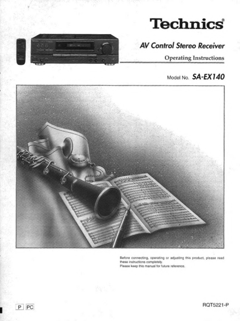
Technics SA-AX910 User manual

Technics

Technics SA-AX910 User manual

Technics SA-AX730 User manual

Technics

Technics SA-AX730 User manual

Technics SAAX6 - RECEIVER User manual

Technics

Technics SAAX6 - RECEIVER User manual

Technics SU-CH700 User manual

Technics

Technics SU-CH700 User manual

Technics SA-616M User manual

Technics

Technics SA-616M User manual

Technics SAEX140 - RECEIVER User manual

Technics

Technics SAEX140 - RECEIVER User manual

Technics SAAX6 - RECEIVER User manual

Technics

Technics SAAX6 - RECEIVER User manual
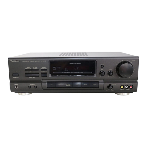
Technics QUARTZ SA-R330 User manual

Technics

Technics QUARTZ SA-R330 User manual

Technics QUARTZ SA-R177 User manual

Technics

Technics QUARTZ SA-R177 User manual

Technics SA-EX300 User manual

Technics

Technics SA-EX300 User manual

Technics SA-EX100 User manual

Technics

Technics SA-EX100 User manual

Technics SA-GX170 User manual

Technics

Technics SA-GX170 User manual
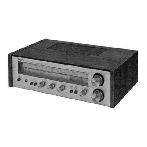
Technics SA-GX350 User manual

Technics

Technics SA-GX350 User manual

Technics SA-GX670 User manual

Technics

Technics SA-GX670 User manual

Technics SA-GX100L User manual

Technics

Technics SA-GX100L User manual

Technics SA-EX700 User manual

Technics

Technics SA-EX700 User manual

Technics SA-5570 User manual

Technics

Technics SA-5570 User manual

Technics SA-AX7 User manual

Technics

Technics SA-AX7 User manual

Technics SADX930 - RECEIVER User manual

Technics

Technics SADX930 - RECEIVER User manual

Technics SA-EX100 User manual

Technics

Technics SA-EX100 User manual

Technics SA-5570 User manual

Technics

Technics SA-5570 User manual

Technics SA-AX920 User manual

Technics

Technics SA-AX920 User manual

Technics SA-500 (DG) User manual

Technics

Technics SA-500 (DG) User manual

Technics SA-110 User manual

Technics

Technics SA-110 User manual
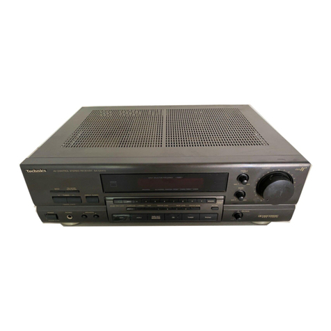
Popular Stereo Receiver manuals by other brands

Lafayette LR-120DB OPERATING & SERVICE MANUAL

Lafayette

Lafayette LR-120DB OPERATING & SERVICE MANUAL

Onkyo TX-8211 instruction manual

Onkyo

Onkyo TX-8211 instruction manual

Yamaha AVENTAGE RXA880BL owner's manual

Yamaha

Yamaha AVENTAGE RXA880BL owner's manual

Onkyo TX-SR803 Specification sheet

Onkyo

Onkyo TX-SR803 Specification sheet

Denon ADV-700 operating instructions

Denon

Denon ADV-700 operating instructions

Rotel RSX-1065 owner's manual

Rotel

Rotel RSX-1065 owner's manual

Denon AVR-X3700H quick start guide

Denon

Denon AVR-X3700H quick start guide

Sony STR-DE997 - Fm Stereo/fm-am Receiver operating instructions
Sony

Sony STR-DE997 - Fm Stereo/fm-am Receiver operating instructions

Denon AVR-1312 Getting started

Denon

Denon AVR-1312 Getting started

Sony STR-DA2100ES Operating Instructions for... Specifications

Sony

Sony STR-DA2100ES Operating Instructions for... Specifications

Denon AVR-X1600H quick start guide

Denon

Denon AVR-X1600H quick start guide

Pioneer VSX-1130-K reference guide

Pioneer

Pioneer VSX-1130-K reference guide

Sony ST-RDE597 Easy setup guide

Sony

Sony ST-RDE597 Easy setup guide

Rockford Fosgate Punch PMX-2 Installation & operation

Rockford Fosgate

Rockford Fosgate Punch PMX-2 Installation & operation

Denon AVR-X3700H owner's manual

Denon

Denon AVR-X3700H owner's manual

Belar FMRR-4 Guide to operations

Belar

Belar FMRR-4 Guide to operations

Sony STR-V 25 Service manual

Sony

Sony STR-V 25 Service manual

Naxa NPB-429 quick start guide

Naxa

Naxa NPB-429 quick start guide

manuals.online logo
manuals.online logoBrands
  • About & Mission
  • Contact us
  • Privacy Policy
  • Terms and Conditions

Copyright 2025 Manuals.Online. All Rights Reserved.