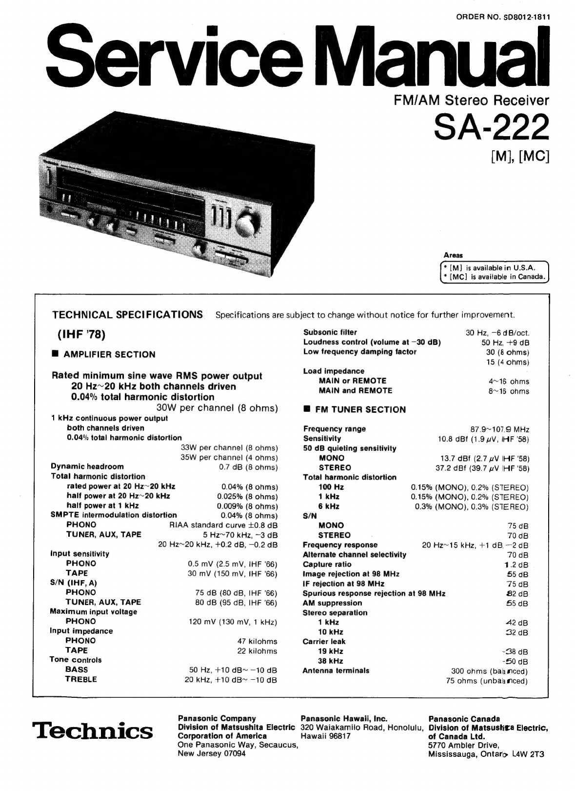
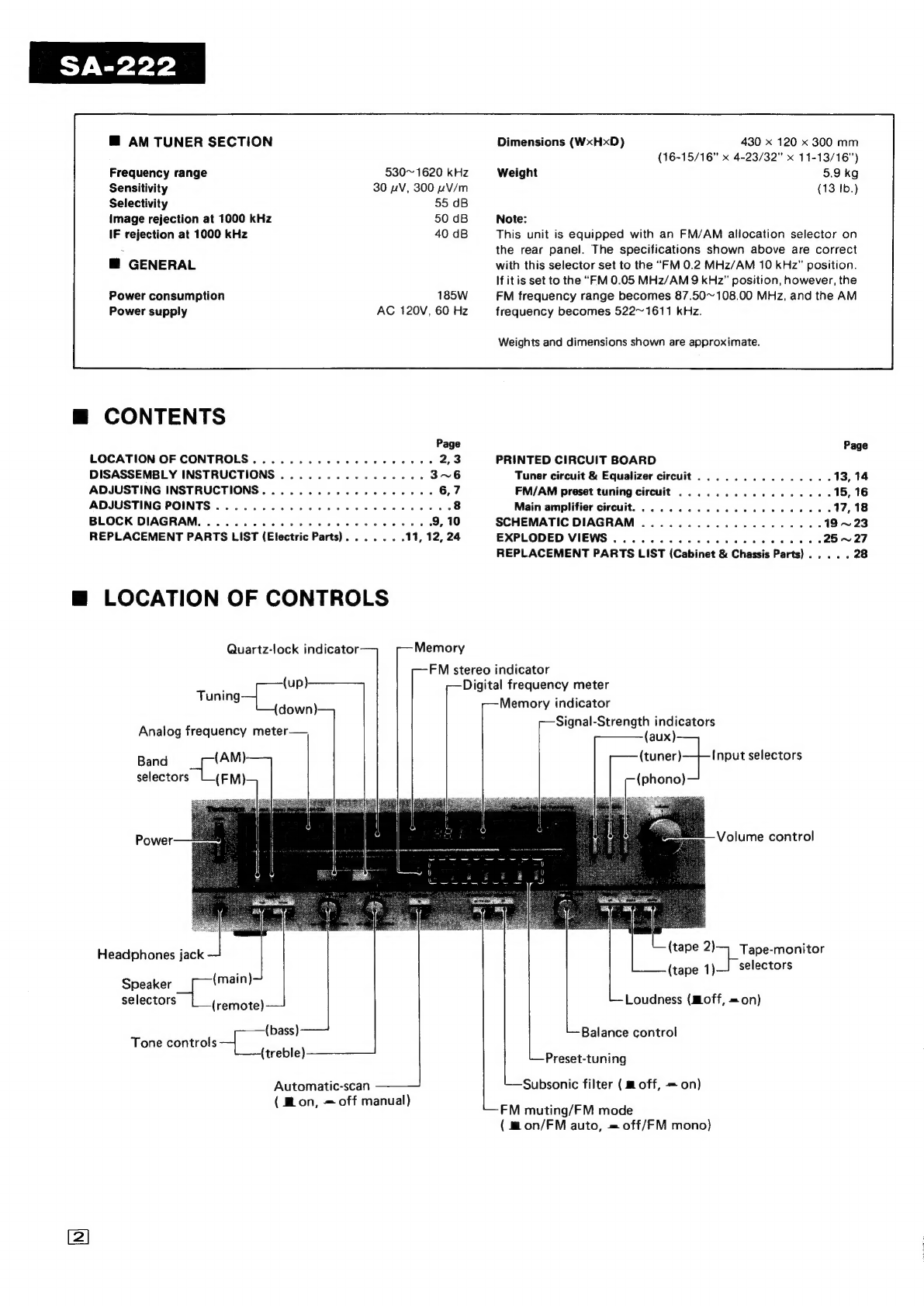
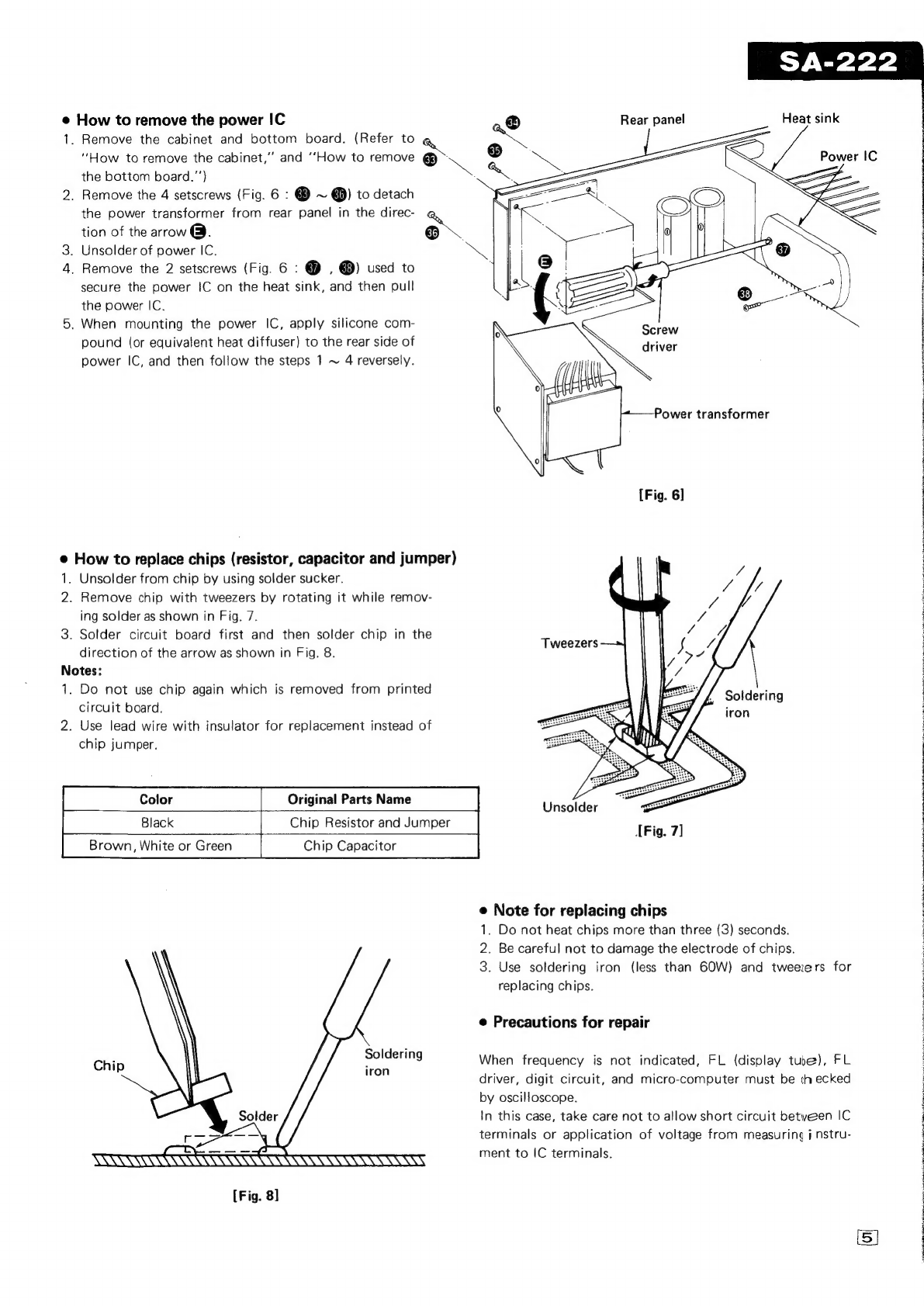
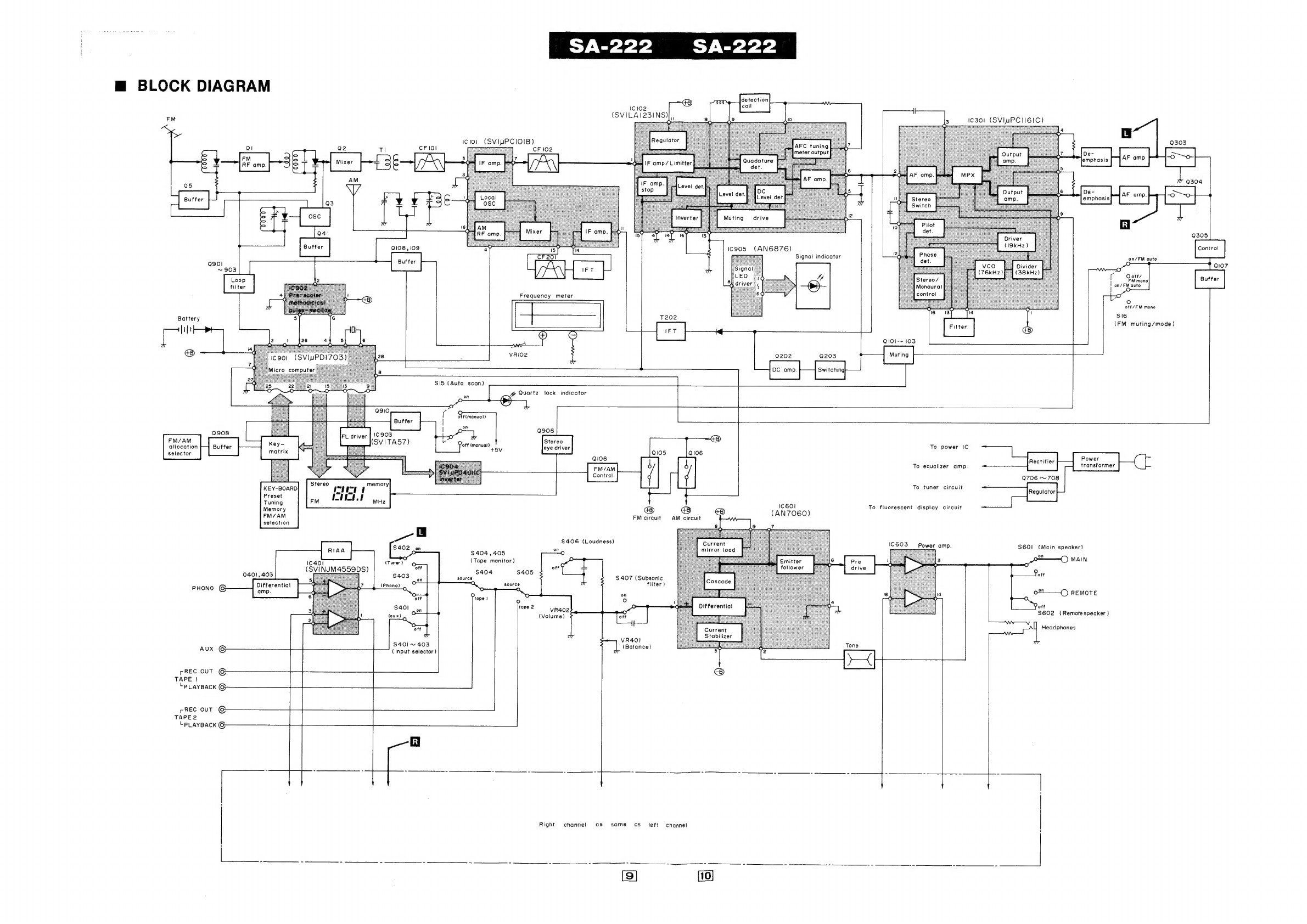
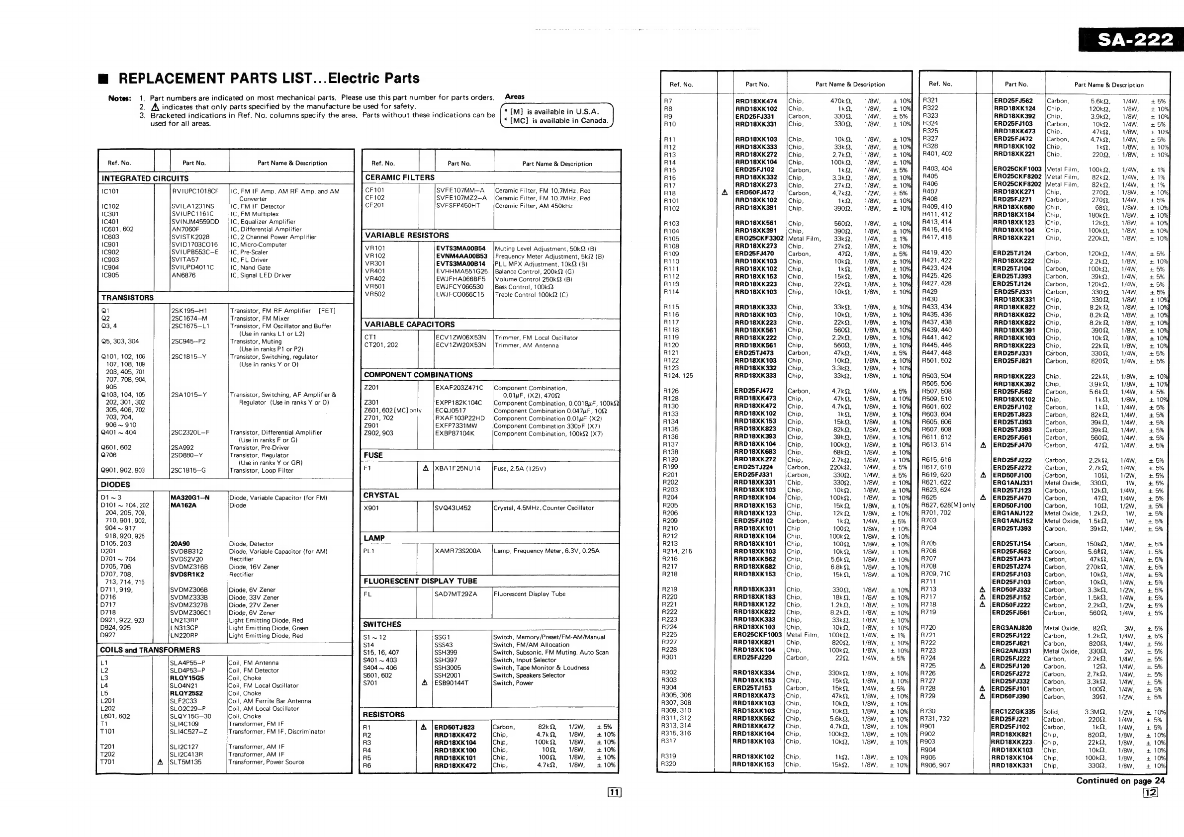
Technics SA-222 User manual
Other Technics Stereo Receiver manuals

Technics
Technics SA-700 - service User manual

Technics
Technics SA-GX470 User manual

Technics
Technics SAAX6 - RECEIVER User manual

Technics
Technics SA-GX230 User manual

Technics
Technics SAEX310 - RECEIVER User manual

Technics
Technics SA-GX530 User manual

Technics
Technics SA-616M User manual

Technics
Technics SA-DX1050 User manual

Technics
Technics SA-GX190 User manual

Technics
Technics SADX930 - RECEIVER User manual

Technics
Technics SA-GX550 User manual

Technics
Technics SA-DA10 User manual

Technics
Technics SC-EH760 User manual

Technics
Technics SA-GX190 User manual

Technics
Technics SA-EX100 User manual

Technics
Technics QUARTZ SA-160 User manual

Technics
Technics SA-GX550 User manual

Technics
Technics SA-AX7 User manual

Technics
Technics SAEX140 - RECEIVER User manual

Technics
Technics SA-AX910 User manual


Popular Stereo Receiver manuals by other brands


Pioneer
Pioneer SX-1000TA operating instructions

Yamaha
Yamaha MusicCast TSR-5B3D owner's manual

Sony
Sony STR-DE335 - Fm Stereo/fm-am Receiver operating instructions

Sony
Sony STR-DG500 - Multi Channel Av Receiver Service manual

Panasonic
Panasonic AJSD955B - DVCPRO50 STUDIO DECK Brochure & specs

Pioneer
Pioneer SX-838 Service manual