Technologic Systems TS-7250 User manual

TS-7250 User's Manual

Technologic Systems, Inc.
16610 East Laser Drive, Suite 10
Fountain Hills, AZ 85268
TEL 480.837.5200
FAX 480.837.5300
http://www.embeddedARM.com/
This revision of the TS-7250 manual is dated
June, 2005
All modifications from previous versions are listed in Appendix B.
A PDF version of this manual is included on the CD that shipped with your unit(s).
The PDF version includes many active links that may be useful to you.
Copyright © 2005 by Technologic Systems, Inc. All rights reserved.

Table of Contents
1 Product Overview
1.1 About This Manual
1.2 Introduction
1.3 Features and Benefits Summary
1.4 Related Products
2 Memory
2.1 SDRAM
2.2 Battery Backed SRAM
2.3 On-board Flash
2.4 USB Flash Drives
3 Serial Ports
3.1 COM1
3.2 COM2
3.3 RS-485 Support
3.4 RS-485 Quick-Start Procedure
3.5 Automatic RS-485 TX Enable
3.6 Using Automatic RS-485 within Linux
3.7 Adding Serial Ports
4 Digital I/O
4.1 DIO Header
4.2 LCD Header
4.3 Using DIO Header for SPI bus
4.4 LCD Interface
5 A/D Converter
5.1 Cirrus 5 Channel A/D converter
5.2 Interpreting Cirrus A/D converter
5.3 TS optional MAX197 8 channel A/D converter
5.4 Single Sample Acquisition Procedure
6 Matrix Keypad Support
7 Real-Time Clock
8 10/100 Base-T Ethernet Port
9 Linux TCP/IP Configuration
10 Watchdog Timer
11 LED, Jumpers and Push-Button Reset
12 PC/104 Bus Expansion
13 Loading or Transferring Files
13.1 Transferring Files via the Ethernet Port
13.2 Zmodem Downloads
14 Debugging
14.1 Debugging with gdb
14.2 Low-Level Debugging with RedBoot
14.3 Using Other Debuggers
15 Console on TS-7250
16 Software and Support
16.1 Linux OS Support
16.2 Other OS Support
16.3 Development Kit and Supplemental CD
17 Installing the TS-7250
17.1 Electrostatic Discharge (ESD) Precautions
17.2 Setup and Installation Instructions
TS-7250 User's Manual
Technologic Systems
http://embeddedARM.com/
i
6/2005

18 Environmental Specifications
19 Options and Other Features
19.1 Options
19.2 Peripheral Boards
19.3 Accessories
20 Feedback and Updates to the Manual
21 Limited Warranty
22 FCC Advisory Statement
Appendix A: Product Views
Appendix B: User Manual Revisions
Appendix C: System Memory Map
Appendix D: Further References
Appendix E: Schematic
Contact Information
TS-7250 User's Manual
Technologic Systems
http://embeddedARM.com/
ii
6/2005

1 Product Overview
1.1 About This Manual
This manual is intended to provide the user with an overview of the board’s features,
benefits, specifications, and set up procedures. It also contains important safety
information.
1.2 Introduction
The model TS-7250 is a compact, full-featured Single Board Computer (SBC) based on
the Cirrus EP9302 ARM9 CPU. The EP9302 features an advanced 200 MHz ARM920T
processor design with a memory management unit (MMU) that allows support for high-
level operating systems such as Linux, Windows CE, and other embedded operating
systems. The ARM920T's 32-bit architecture, with a five-stage pipeline, delivers very
impressive performance at very low power.
The EP9302 CPU has a 16 KB instruction cache and a 16 KB data cache to provide
zero-cycle latency to the current program and data, or they can be locked to guarantee
no-latency access to critical sections of instructions and data. For applications with
instruction-memory size restrictions, the ARM920T’s compressed Thumb instruction set
can be used to provide higher code density and lower Flash storage requirements.
The TS-7250 CPU integer performance at 200 MHz is about twice as fast as the
Technologic Systems 133MHz 586-based products, but costs half as much!
TS-7250 User's Manual
Technologic Systems
http://embeddedARM.com/
1
6/2005

1.3 Features and Benefits Summary
The TS-7250 comes standard with these features:
●200 MHz ARM9 CPU with MMU
●32MB RAM
●32MB on-board Flash (Boots to Linux)
●10/100 Megabit Ethernet port
●2 USB compliant Full Speed host (OHCI) ports -- (12 Mb/s max)
●2 COM ports (up to 230 Kbaud)
●Watchdog Timer
●PC/104 expansion bus
●SPI bus interface
●20 Digital I/O lines
●Alphanumeric LCD and matrix keypad interface
●Single +5VDC supply @ 400 mA – (under 2 watts)
●Small size -- 3.8 x 4.5 inches (9.7 x 11.5 cm)
These optional features are also available:
●8-channel 12-bit analog-to-digital converter
●Battery-backed Real-Time Clock (TS-5620)
●RS-485 support on COM2 with automatic TX enable
●Temperature sensor
●Additional COM ports
TS-7250 power supply:
The TS-7250 requires regulated 5VDC at 450 mA (typical maximum). It is possible to
lower this power significantly by lowering the CPU clock rate or by powering-down the
Ethernet PHY chip.
A quick release screw-down terminal block for the 5V power and power GND
connections is provided for easy connection to an external power supply.
Note:
Supply voltages over 6 VDC may damage the TS-7250.
Be sure to use a regulated 5 VDC power supply, preferably with current limiting to 1 to
3 Amps. A current limited supply is very forgiving of common errors during
development. A PC power supply that may be capable of supplying 20 Amps or more is
not recommended -- it is possible to do irreversible damage to the TS-7250 if the
polarity on the power leads is reversed.
When power is first supplied to the TS-7250, the board mounted LEDs are immediately
turned on under hardware control. Once the processor begins execution, the LEDs are
turned off. The RED led is briefly turned on while the processor looks for the TS-
BOOTROM stored in the first sector of Flash. If the processor does not find the TS-
BOOTROM, it will turn off the red LED and continuously blink the green LED. If the
LEDs do not turn on at all, the most likely problem is the power supply. Check that the
+5V and GND connections are not reversed. A diode protects the board against
damage in such a situation.
Once the processor has found the TS-BOOTROM, the green LED is turned on just
before jumping to it. The TS-BOOTROM briefly turns off the green, and turns on the
TS-7250 User's Manual
Technologic Systems
http://embeddedARM.com/
2
6/2005

RED, while running the SDRAM initialization and test routines, but otherwise remains
green until RedBoot is called and starts its own initialization. If a problem was detected
with the hardware in the TS-BOOTROM, the LEDs blink alternately red, then green, at a
very fast rate. The red LED is on during RedBoot initialization, and once complete, the
green LED is lit and remains on from that point forward.
1.4 Related Products
Technologic Systems offers an enclosure for the TS-7250. Several daughter boards are
also available that can add functionality via the PC/104 bus. Since the PC/104 bus is an
industry standard, an almost unlimited number of third-party products can be added via
the PC/104 expansion bus.
TS-7250 User's Manual
Technologic Systems
http://embeddedARM.com/
3
6/2005

2 Memory
2.1 SDRAM
The TS-7250 uses 256 Megabit SDRAM technology to provide 32 or 64 Megabytes
(MB) of high-speed RAM. By using the latest SDRAM technology 512 Megabit chip, it is
possible to have 128 MB of RAM on the TS-7250.
The TS-7250 SDRAM chips are soldered directly to the board. By not using socketed
memory, the TS-7250 is much more reliable in high-vibration environments.
The TS-7250 RAM is not contiguous in the physical memory map of the EP9302. But
the MMU is programmed to remap the blocks of RAM to appear as a contiguous block
of memory at the very beginning of the virtual memory map. In the case of a 256
Megabit SDRAM chip (32 MB), it is located at 0 through 32 MB in the virtual memory
map.
2.2 Battery Backed SRAM
There is a daughter board available for the TS-7xxx products (TS-NVRAM) that will
allow adding 32K bytes or 128 Kbytes or 512K bytes of battery-backed SRAM. Battery
backed SRAM provides non-volatile memory with very fast write times and unlimited
write cycles, unlike Flash memory. This can be very important if the data is constantly
being updated several times per minute, since Flash devices can wear-out after a few
million write cycles. It also eliminates the latency that Flash memory has during write
cycles, since Flash technology write cycles are about 10-100 times slower than read
cycles.
The TS-NVRAM daughter card is located at the PC/104 memory space base address of
0x11AA_0000. This resource is a byte-wide memory device using a lithium battery that
is guaranteed to last a minimum of 10 years with or without power applied.
TS-7250 User's Manual
Technologic Systems
http://embeddedARM.com/
4
6/2005

2.3 On-board Flash
The TS-7250 uses a NAND Flash chip for its on-board Flash resource. The first 16KB is
reserved for the TS-BOOTROM code. The TS-BOOTROM code initializes various
internal configuration registers for proper operation for the TS-7250 design and
initializes and tests the SDRAM. The last 3 MB are reserved for the RedBoot ROM
monitor, RedBoot FIS (Flash Image System) and RedBoot FCONFIG (Flash config).
The default shipping Linux kernel is pre-loaded in the FIS and the default boot script
and Ethernet MAC address are contained in the FCONFIG. You may also use the
RedBoot FIS to store and load Flash images that contain eCos applications or other OS/
RTOS bootloaders. The rest of the on-board flash is used for the YAFFS2 file system.
This is a journaling file system that is aware of the wear-out mechanism of the NAND
flash and incorporates ECC algorithms at the file system level to maximize Flash
lifetime. It is also extremely tolerant of power failures during file write sequences.
The physical address of the Flash chip is 0x6000_0000. It is possible to use larger sizes
of the NAND Flash than the standard 32 MB chip. The TS-7250 is designed to
accommodate both 32 MB and 128 MB chips. Please call Technologic Systems for
larger Flash sizes.
The entire Flash chip can be write-protected by removing Jumper #3. When JP3 is not
installed the Flash chip becomes a read-only resource.
2.4 USB Flash Drives
Additional non-volatile storage can be added with a USB Flash drive. USB Flash drives
can supply additional storage, either for additional data storage or to host a complete
Operating System, such as Debian. A tar-file of Debian is available on the Technologic
Systems website. Alternatively, the developer's kit can include a USB flash thumb-drive
pre-loaded with Debian.
After booting into the demonstration TSLinux Operating System hosted on the NAND
Flash, one can 'boot' into the Debian OS with two scripts found on the demonstration
TSLinux Operating System. First, invoke /usr/bin/loadUSBModules.sh, then run the
script /usr/bin/loadUSB.sh to chroot into the Debian OS to take full advantage of such
things as the Debian arm-toolchain.
Note:
Drivers are available in the TS-Linux distribution to support USB Flash Drives.
TS-7250 User's Manual
Technologic Systems
http://embeddedARM.com/
5
6/2005

3 Serial Ports
The TS-7250 has two asynchronous serial ports (COM1 and COM2) provide a means to
communicate with external serial devices. Each is independently configured as a
16C550- type COM port that is functionally similar to a standard PC COM port. These
ports have 16-byte FIFOs in both the receive and the transmit UART channels.
Both COM ports can support all standard baud rates up through 230.4Kbaud. Both
COM ports may be configured to use a DMA channel (useful when very high baud rates
are being used).
Either UART can generate:
●four individually-maskable interrupts from the receive, transmit, and modem
status logic blocks
●a single, combined interrupt that is asserted if any of the individual interrupts are
asserted and unmasked
COM1 can also the support HDLC protocol -- Download the EP9301 User Guide for
more details.
COM2 can optionally support RS-485 half or full duplex levels.
3.1 COM1
Table 3.1 COM1 DB9 Pin-Outs
DB9 Pin Signal Description
1 DCD Data Carrier Detect
2 RXD Receive Data
3 TXD Transmit Data
4 DTR Data Terminal Ready
5 GND Ground
6 DSR Data Set Ready
7 RTS Request to Send
8 CTS Clear to Send
9 -- --
The base address of COM1 appears in the physical
address space at 0x808C_0000.
COM1 has RS-232 support for the following signals:
●TXD
●RXD
●RTS
●CTS
●DTR
●DSR
●DCD
This full complement of RS-232 signals (all except
Ring Detect) allows COM1 to interface to almost
any serial RS-232 device.
The COM1 RS-232 port uses a DB-9 male connector on the TS-7250. See Table 3.1 for
a list of COM1 pin-outs.
TS-7250 User's Manual
Technologic Systems
http://embeddedARM.com/
6
6/2005
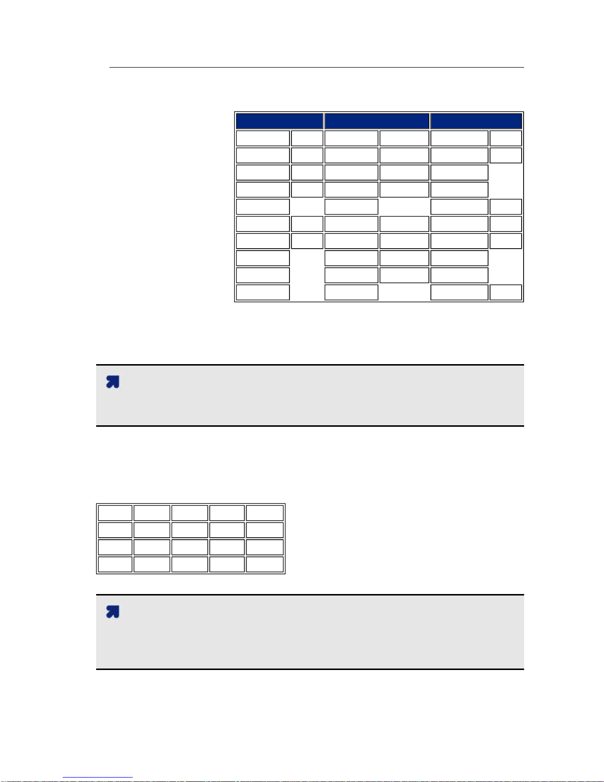
3.2 COM2
Table 3.2a COM2 Serial Port Header Pin-Outs
RS-232 Half Duplex RS-485 Full Duplex RS-485
9-Pin SubD Signal 9-Pin SubD Signal 9-Pin SubD Signal
1 1 TX+ / RX+ 1 TX+
2 RXD 2 2
3 TXD 3 3
4 4 4 RX+
5 GND 5 GND 5 GND
6 6 TX- / RX- 6 TX -
7 7 7
8 8 8
9 9 9 RX -
The base address of
COM1 appears in the
physical address space
at 0x808D_0000.
COM2 has RS-232
support only for the TXD
and RXD signals. This is
sufficient to interface
with serial devices that
only require transmit
and receive data lines.
COM2 is accessible on
a 10-pin header labeled
COM2. Adaptor cables
are available to convert
these into standard 9-
pin SubD male connectors.
In addition, COM2 has optional support for full or half-duplex RS-485. See Table 3.2a
for COM2 pin-outs.
Note:
The COM2 serial port 10-pin header has both RS-232 and RS-485 signals. Only one
set is in use for a given application – it is not possible to use both at the same time.
The pin-outs for the COM2 10-pin header are listed in Table 3.2b. (NC = No Connection)
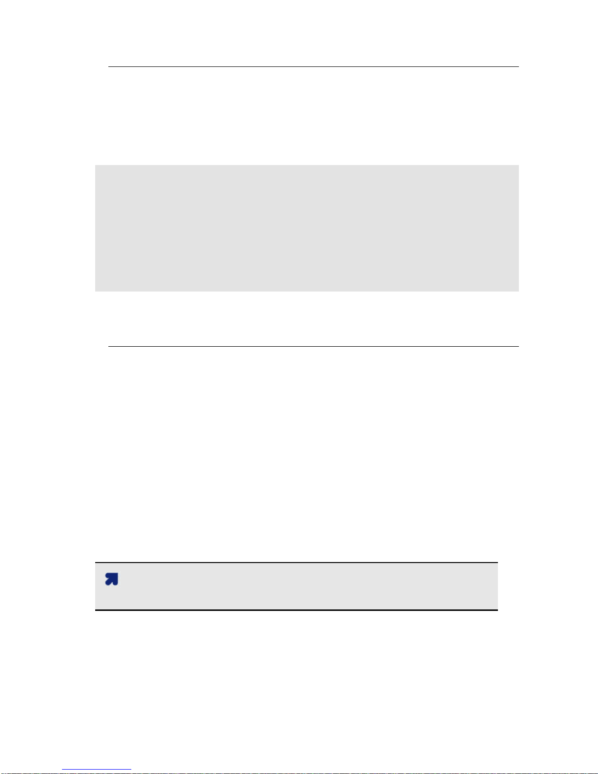
Table 3.2b COM2 Serial Port Header Pin-
Out (showing non-standard numbering
scheme)
TX- RX- NC NC TX-
6 7 8 9 10
1 2 3 4 5
TX+ RXD RXD RX+ GND
Note:
The COM2 serial port header uses a non-standard numbering scheme, as shown in
table 3.2b. This was done so the header pins would have the same numbering as the
corresponding DB-9 pin; i.e. pin 3 (TXD) on the header connects to pin 3 on the DB-9.
TS-7250 User's Manual
Technologic Systems
http://embeddedARM.com/
7
6/2005

3.3 RS-485 Support
An option is available to add support to COM1 for half duplex or full duplex RS-485. RS-
485 drivers allow communications between multiple nodes up to 4000 feet (1200
meters) via twisted pair cable. Half-duplex RS-485 requires one twisted pair plus a
Ground connection, while full duplex requires two twisted pair plus a Ground.
For half-duplex operation, a single twisted pair is used for transmitting and receiving.
The Auto485.exe utility must be run to initialize the automatic RS-485 control logic. For
full-duplex operation, two twisted pairs are used and the transmit driver is typically
enabled all the time. The auto485.exe utility must be run to put the logic into full-duplex
RS-485 mode.
Fail-safe bias resistors are used to bias the TX+, TX- and RX+, RX- lines to the correct
state when these lines are not being actively driven. This is an important consideration,
since in a typical RS-485 installation, the RS-485 drivers are frequently tri-stated. If fail-
safe bias resistors are not present, the 485 bus may be floating and very small amounts
of noise can cause spurious characters at the receivers. 4.7KW resistors are used to
pull the TX+ and RX+ signals to 5V and also to bias the TX- and RX- signals to ground.
Termination resistors in many installations are not required when cable lengths are less
than 50 meters and the baud rate is 9600 or less. Termination resistors may be required
for reliable operation when running longer distances or at higher baud rates.
Termination resistors (typically 100-150 ohms) should only be installed at each end of
an RS-485 transmission line. In a multi-drop application where there are several drivers
and/or receivers attached, only the devices at each end of the transmission line pair
should have termination resistors.
A read at I/O location 0x2240_0000 bit 1 will return a "1" when the RS-485 option is
installed.
3.4 RS-485 Quick-Start Procedure
Perform the following steps:
1. Check that the RS-485 option is installed in the TS-7250 (required).
2. Attach the RS-485 cable to the 10-pin header. (Adaptor cables to SubDB9
connector are available from Technologic Systems.)
3. Set the COM2 UART serial parameters (baud rate, data, parity, and stop bits,
interrupts, etc) in your source code
4. Use the TIOC_SBCS485 ioctl() to enable the automatic RS-485 feature.
5. Simply read () and write () data to the COM2 UART – the automatic RS-485 logic
controls TX enable.
TS-7250 User's Manual
Technologic Systems
http://embeddedARM.com/
8
6/2005

3.5 Automatic RS-485 TX Enable
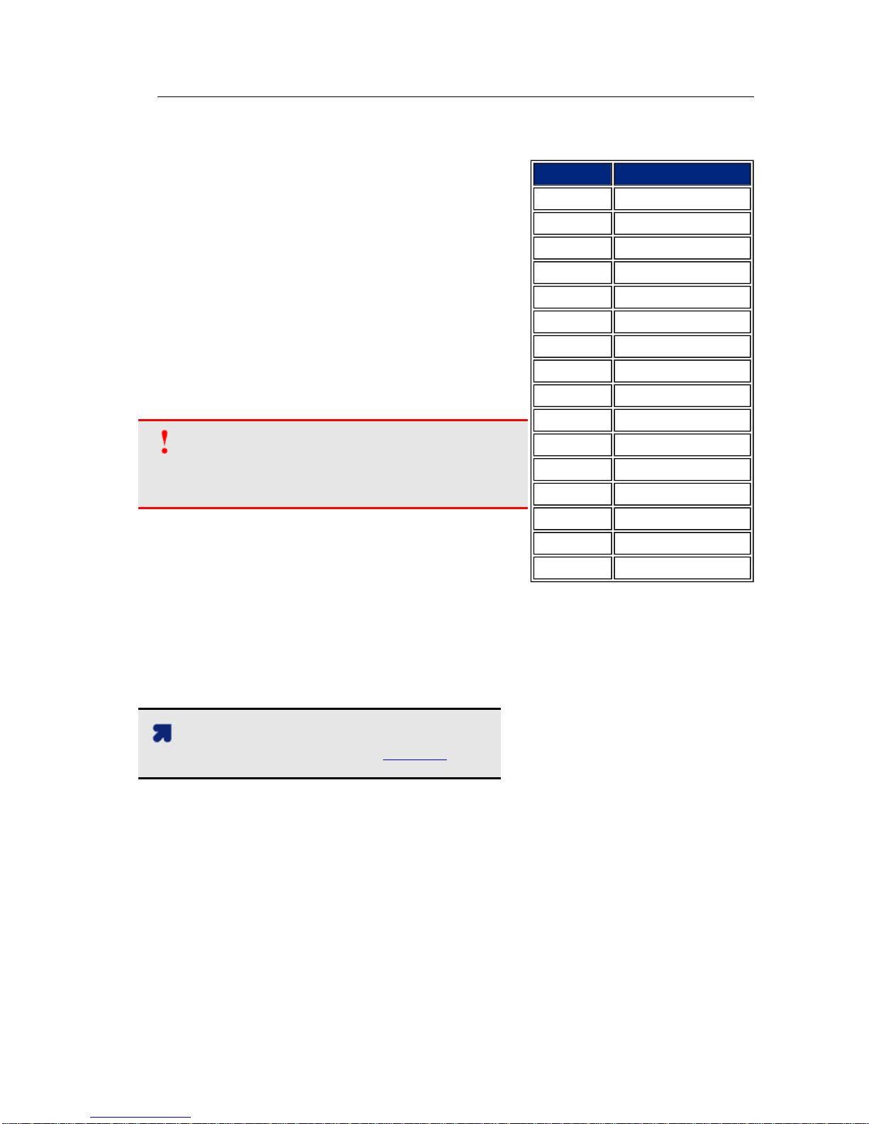
Table 3.5 COM2 Mode Register
Value (Hex) MSB MID LSB Mode
00 0 0 0 RS-232
01 0 0 1 Full-Duplex RS-485
02 0 1 0 -- Reserved
03 0 1 1 -- Reserved
04 1 0 0 Half-Duplex 9600 baud
05 1 0 1 Half-Duplex 19.2Kbaud
06 1 1 0 Half-Duplex 57.6Kbaud
07 1 1 1 Half-Duplex 115.2Kbaud
TS-7250 supports fully automatic
TX enable control under hardware
control. This simplifies the design
of half-duplex systems since
turning off the transmitter and
enabling the receiver in software is
typically difficult to implement. If
this is implemented in software,
then the COM2 UART transmit
holding register and the transmit
shift register both must be polled
until empty before deasserting the
TX enable signal to the RS-485
driver. The design gets more
complicated when using the TX FIFO or when using a multi-tasking OS such as Linux.
The implementation on the TS-7250 uses hardware in a Xilinx PLD to automatically
control when the RS-485 drivers and receivers are selected. The automatic RS-485
logic eliminates the need for any software polling and supervision. A counter in the
Xilinx PLD is used to keep track of the bits shifting out the COM2 UART. This circuit
automatically turns on/off the RS-485 transceiver and receiver at the correct times. This
only requires the COM2 Mode registers in the PLD to be initialized once based on baud
rate and data format.
COM2 will default to RS-232 mode at reset (COM2 mode register = Hex 00). In order to
switch COM2 into Full duplex RS-485 mode, the COM2 Mode register at 0x22C0_0000
must be set to Hex 01. In this mode, the TX drivers are always asserted.
In order to switch COM2 into half-duplex RS-485, then the COM2 mode register at
0x22C0_0000 must be set to Hex 04, 05, 06 or 07 depending upon the baud rate
required. Baud rates of 9600, 19.2K, 57.6K and 115.2K are supported. If you need to
operate COM2 in half-duplex RS-485 at any other baud rate, then contact Technologic
Systems.
A second COM2 Mode register at 0x2300_0000 must be set to Hex 01 if the COM2 is in
half-duplex mode and the data format is using 8 data bits with parity or 8 data bits with 2
stop bits.
Note:
COM2 can support half-duplex RS-485 baud rates of 9600, 19.2K, 57.6K and
115.2Kbaud. For any other baud rate, contact Technologic Systems.
TS-7250 User's Manual
Technologic Systems
http://embeddedARM.com/
9
6/2005
3.6 Using Automatic RS-485 within Linux
A special ioctl command has been added to the Linux kernel's serial code to turn off and
on the automatic RS-485 feature. The header files needed to be included from the Linux
kernel source tree and an applications source code are linux/ts_sbc.h and linux/include/
asm/ioctls.h. These header files can be found in a Linux kernel patched with an
appropriate patch from Technologic Systems. The following snippet of code
demonstrates the use of this ioctl.
#include <linux/ts_sbc.h>
#include <linux/include/asm/ioctls.h>
<snip>
mcr = AUTO485FD
//mcr = AUTO485HD //for half duplex
ioctl (fd, TIOC_SBCS485, &mcr);
//write() and read() from fd
ioctl (fd, TIOC_SBCC485, &mcr);
//further reads() and writes() may not behave
3.7 Adding Serial Ports
If your project requires more than two serial ports, additional ports may be added via the
PC/104 expansion bus. Technologic Systems offers three different daughter boards (TS-
SER1, TS-SER2, and TS-SER4) that add 1, 2, or 4 extra COM ports respectively.
These can be configured using PC designations COM1, COM2, or higher. These will
appear in the TS-7250 PC/104 address space (0x11A0_0000 base address). For
example, a TS-SER1 daughter board can be jumper selected as COM3 which would
correspond to a PC I/O base address of 0x3E8. On the TS-7250, this COM port will
appear at the physical base address of 0x11A0_03E8.
The TS-7250 PC/104 expansion bus has IRQ5, IRQ6, and IRQ7 available for additional
serial port interrupts.
Typically each serial port has a dedicated interrupt, but the TS-SER4 daughter board
allows all four extra serial ports to share a single interrupt. This is very helpful in
systems with a large number of serial ports since there are a limited number of IRQ
lines available.
Note:
Drivers are available in the TS-Linux distribution to support these extra COM ports.
TS-7250 User's Manual
Technologic Systems
http://embeddedARM.com/
10
6/2005

4 Digital I/O
There are 20 Digital Input/Output (DIO) lines available on the TS-7250. These are
available on two headers labeled “DIO” and “LCD”. The header labeled LCD can be
used as 11 DIO lines or as an alphanumeric LCD interface (See Section 4.2). The
header labeled DIO has 9 DIO pins available. In addition to the DIO signals, each
header also has a power pin and Ground available. The LCD header has 5V power
available while the DIO header has 3.3V power.
Three pins on the DIO header are used to bring out the EP9302 SPI bus. By using
some of the DIO pins as peripheral Chip Select signals, a complete interface is
available for SPI peripherals. It is also possible to bring out a fourth SPI bus function
[SPI_Frame] by adding a 10 ohm resistor in the position labeled R1 on TS-7250 RevB
boards. This signal is not required for many SPI peripherals but it may prove useful in
some applications.
All of the DIO lines are programmable as either inputs or outputs and the direction of
each I/O pin can be individually programmed. All DIO control registers are 8-bits wide
and aligned on word (32-bit) boundaries. For all registers, the upper 24 bits are not
modified when written and are always read back as zeros. Every DIO pin has two
registers used to access it, an 8-bit data register and an 8-bit data direction register
(DDR). The DDR controls whether each DIO pin is an input or an output (”1” = output).
Writing to the data register only affects pins that are configured as outputs. Reading the
data register always returns the state of the DIO pin.
Many of the DIO pins (DIO_0 thru DIO_8 and LCD_0 thru LCD_7) can also be
programmed to cause interrupts. The interrupt properties of these pins are individually
configurable -- each interrupt can be either high or low level sensitive or either rising or
falling edge triggered. It is also possible to enable debouncing on any of these
interrupts. Debouncing is implemented using a 2-bit shift register clocked by a 128 Hz
clock. Download the EP9301 User Manual and see Chapter 21 for details.
The TS-7250 RevB boards also allow access to two 12-bit A/D channels on the DIO
header.
The 5V power output pin on the LCD header has a 750 mA Poly-Fuse to prevent
excessive current. The 3.3V power on the DIO header is current limited to
approximately 1 Amp by an LM1117 3.3V regulator.
TS-7250 User's Manual
Technologic Systems
http://embeddedARM.com/
11
6/2005
4.1 DIO Header
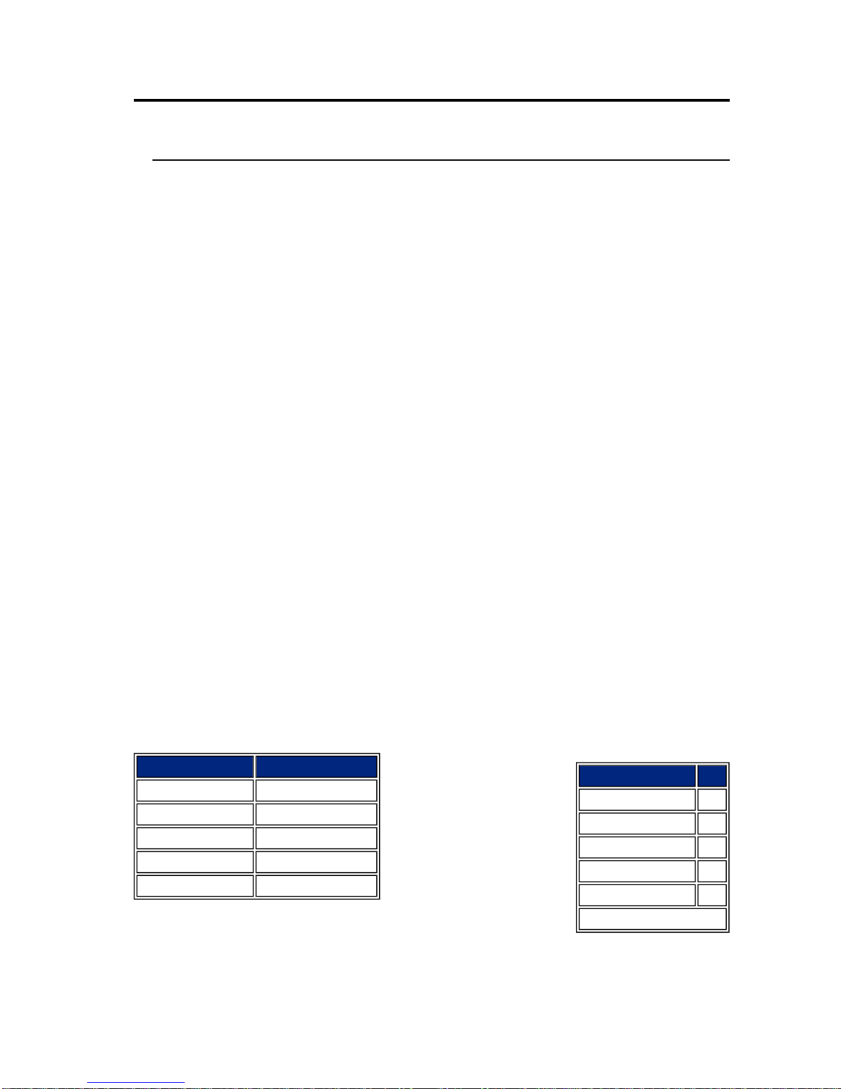
Table 4.1 DIO Header Pin-Out
Header Pin Description
1 DIO_0
2 GND
3 DIO_1
4 1000 mA driver (bit 0)
5 DIO_2
6 SPI_Frame
7 DIO_3
8 DIO_8
9 DIO_4
10 SPI_MISO
11 DIO_5
12 SPI_MOSI
13 DIO_6
14 SPI_CLK
15 DIO_7
16 3.3 V
The DIO port provides +3.3V, GND, the SPI bus, and 9
digital I/O lines that may be used to interface the TS-7250
with a wide range of external devices. DIO lines DIO_0
thru DIO_7 are a byte-wide port using Port B on the
EP9302 and are accessed via the data register at
physical address location 0x8084_0004. The DDR for this
port is at 0x8084_0014.
DIO_8 is accessed via bit 0 of Port F in the EP9302 and
is accessed via the data register at physical address
location 0x8084_0030. The DDR for this port is at
0x8084_0034. It is important not to change the other bit
positions in these Port F registers since these other DIO
pins are being used on the TS-7250. All accesses to
these registers should use read-modify-write cycles.
Warning:
All pins on the DIO header use 0-3.3V logic
levels. Do not drive these lines to 5V.
When the DIO pins are configured as outputs, they can
source 4 mA or sink 8 mA and have logic swings
between 3.3V and ground. When configured as inputs,
they have standard TTL level thresholds and must not be
driven below 0 Volts or above 3.3 Volts. DIO lines DIO_0 thru DIO_3 have 4.7 KW pull-
up resistors to 3.3V biasing these signals to a logic”1”. The other DIO pins have 100 KW
bias resistors biasing these inputs to a logic “1”.
DIO signals DIO_0 thru DIO_7 are physically arranged to allow a 16-pin (2x8) ribbon
cable to directly connect a 4x4 matrix keypad. Drivers are available for this interface.
Note:
The SPI interface is described in section 4.3.
A/D Converter
The DIO Port pins 4 and 6 are connected to two of the EP9302 12-bit A/D converter
inputs. These can be used to measure analog signals in the range of 0 to 3.3V.
TS-7250 User's Manual
Technologic Systems
http://embeddedARM.com/
12
6/2005

4.2 LCD Header
Table 4.2 LCD Header
Pin-Out
Header Pin Description
1 5V
2 GND
3 LCD_RS
4 Bias
5 LCD_EN
6 LCD_WR
7 LCD_1
8 LCD_0
9 LCD_3
10 LCD_2
11 LCD_5
12 LCD_4
13 LCD_7
14 LCD_6
The LCD Port can be used as 11 additional digital I/O lines or it
can be used to interface to a standard alphanumeric LCD display.
The header has been arranged to allow a 14-pin ribbon cable to
directly connect to industry standard LCD displays. Technologic
Systems has available a 2x24 LCD display with software drivers
for rapid development.
DIO lines LCD_0 thru LCD_7 are a byte-wide port using Port A on
the EP9302 and are accessed via the data register at physical
address location 0x8084_0000. The DDR for this port is at
0x8084_0010.
Since this port is interfacing to a 5V LCD, 1.0 KW resistors have
been added in series between the EP9302 and the LCD_0 thru
LCD_7 pins. This is required since the LCD data bus could be
driving these lines above 3.3V. The series resistors prevent the
LCD from overdriving the EP9302 Port A pins. If using these pins
for general purpose DIO, the current sourcing and sinking
capability of these DIO pins is limited by the 1.0 KW resistors.
LCD_EN, LCD_ RS , and LCD_WR are DIO pins using EP9302
Port H bits 3 through 5 respectively and are accessed via the data
register at physical address location 0x8084_0040. The DDR for
this port is at 0x8084_0044. When these DIO pins are configured
as outputs, they can source 4 mA or sink 8 mA and have logic swings between 3.3V
and ground. When configured as inputs, they have standard TTL level thresholds and
must not be driven below 0 Volts or above 3.3 Volts. These DIO pins have 100 KW bias
resistors biasing these inputs to a logic “1”. It is important not to change the other bit
positions in these Port H registers since the other DIO pins are being used on the TS-
7250. All accesses to these registers should use read-modify-write cycles.
Warning:
LCD pins 3, 5, and 6 use 0-3.3V logic levels. Do not drive these lines to 5V.
Pin 4 on this header (labeled Bias) is a 620 ohm resistor to ground for LCD contrast
biasing.
The 5V power on the LCD header has a 750 mA Poly-Fuse to limit the current.
TS-7250 User's Manual
Technologic Systems
http://embeddedARM.com/
13
6/2005

4.3 Using DIO Header for SPI Bus
Table 4.3 DIO Header Pin-Outs
Header Pin Name Function
10 SPI_MISO Master Output /
Slave Input
12 SPI_MOSI Master Output /
Slave Input
14 SPI_CLK Clock
6 SPI_Frame SPI Frame pin
The EP9302 Synchronous Serial
Port is available on the DIO
header. This port can implement
either a master or slave interface
to peripheral devices that have
either Motorola SPI or National
Semiconductor Microwire serial
interfaces. The transmit and
receive data paths are buffered
with internal FIFO memories
allowing up to eight 16-bit values
to be stored for both transmit and receive modes. The clock rate is programmable up to
3.7 MHz and has programmable phase and polarity. The data frame size is
programmable from 4 to 16 bits.
By using some of the DIO Header pins as peripheral Chip Select signals, a complete
interface is available for addressing up to 9 SPI peripherals. The SPI bus pins are
defined in the table below.
Warning:
The SPI bus pins use 0-3.3V logic levels. Do not drive these lines to 5V.
Download the EP9301 User’s Manual and see Chapter 19 for more details on using the
SPI bus.
TS-7250 User's Manual
Technologic Systems
http://embeddedARM.com/
14
6/2005

4.4 LCD Interface
Table 4.4a LCD Header Signals
PIN Function Comments
1 LCD 5V LCD Power
2 LCD_GND
3 LCD_RS Register select
4 Bias 620 Ohm to GND
5 LCD_EN Active high enable
6 LCD_WR# Active low write
7 LCD_D1 D0 - D7:
Buffered
bi-directional
data bus
8 LCD_D0
9 LCD_D3
10 LCD_D2
11 LCD_D5
12 LCD_D4
13 LCD_D7
14 LCD_D6
A 14-pin LCD connector is provided on the
TS-7250 for interfacing with standard
alphanumeric LCD displays. These displays
use a common controller, the Hitachi
HD44780 or equivalent. While software
written for the HD44780 works with all
displays using the controller, the cable
needed is dependent on the display used.
For most displays, a straight-through type
ribbon cable can be used. The connector on
the LCD display is typically mounted on the
backside of the display.
Warning:
Using an incorrect cable or
mounting the LCD connector on the
front-side can result in a reverse
power polarity and can damage the
LCD display. Please refer to your
LCD data sheets for in-depth
information.
Technologic Systems has available a 2x24 LCD display with software drivers for rapid
development.
Table 4.4b LCD
Header Pin-Outs
2468101214
13579 1113
The pin-outs in the above table are not the standard given for LCD
displays. However, these pin-outs allow a standard ribbon cable to
be used when the ribbon cable is attached to the backside of the
LCD.
Sample code is available for the LCD. Contact Technologic Systems
for more information.
TS-7250 User's Manual
Technologic Systems
http://embeddedARM.com/
15
6/2005
5 A/D Converter
5.1 Cirrus 5 Channel A/D Converter
The Cirrus EP9302 features a 5 channel, 12-bit Analog to Digital Converter with an
analog multiplexor, with an input range of 0 to 3.3 V. The Cirrus A/D converter can do a
maximum of 925 samples per second, and requires a settling time of 2 milliseconds
between channel switches. The EP9302 A/D converter is standard on all TS-7250. Note
that the Cirrus A/D converter is not the same as the optional, full-featured MAX197 A/D
converter. To maintain 12-bit accuracy, the analog signal being measured must have a
low source impedance (less than 10 ohms). Otherwise, an operational amplifier may
need to be added to buffer the A/D input. The EP9302 A/D converter should not be
driven by a source impedance greater than 10 ohms to ensure accurate results (the
Cirrus A/D converter has an input impedance that is not completely linear and may be
as low as 10K ohms). For detailed information, please see the Cirrus EP9302 User's
Guide, page 518, as well as the Cirrus EP9315 User's Manual, page 53. For high-
performance applications, the optional MAX197 A/D converter is preferred.
The following steps outline how to use the Cirrus A/D converter
1. Unlock the software lock before setting the TSEN bit in the ADCClk register by
writing 0xAA to the ADCSWLock register (0x8090_00C0 )
2. OR in the TSEN bit (bit 31) to the ADCClkDiv register (0x8093_0090)
3. Unlock the software lock (again) before OR'ing in the ADCEN (ADC clock enable,
bit 31) to 0x8093_0080
4. Clear bit 2, the ADCPD (ADC Power Down) bit, at 0x8093_0080. This bit MUST
be set to 0 (see page 91 of the EP9301 user's manual)
5. After unlocking the software lock, write the channel's magic value (see the
following table, or Cirrus EP9301 User's Guide, table 20-2) to the ADCSwitch
register (0x8090_0018) to select that channel for the next data acquisition
6. Poll the ADCResult register (0x8090_0008) until bit 31 is not set
7. Using a 32 bit read operation, read the result from 0x8090_0008, masking off the
upper 16 bits
Table 5.1b Onboard
ADC Header Signals
ADC Channel Pin
0 1
1 3
2 5
3 7
4 9
all even pins are ground
Table 5.1 Cirrus ADCSwitch Values
Input to Measure ADCSwitch Value
ADC0 0x0000_0608
ADC1 0x0000_0680
ADC2 0x0000_0640
ADC3 0x0000_0620
ADC4 0x0000_0610
TS-7250 User's Manual
Technologic Systems
http://embeddedARM.com/
16
6/2005
Table of contents
Other Technologic Systems Motherboard manuals

Technologic Systems
Technologic Systems TS-7300 User manual

Technologic Systems
Technologic Systems TS-2800 User manual

Technologic Systems
Technologic Systems TS-3100 User manual

Technologic Systems
Technologic Systems TS-7200 User manual

Technologic Systems
Technologic Systems TS-5300 User manual

Technologic Systems
Technologic Systems TS-3300 User manual

Technologic Systems
Technologic Systems TS-72XX series User manual

Technologic Systems
Technologic Systems TS-5700 User manual


