Acorp 6ZX85 User manual

The information presented in this publication has been made
carefully for reliability; however, no responsibility is assumed
for inaccuracies. Specifications are subject to change without
notice.
IBM, PC/AT, and PC/XT are trademarks of International Busi-
ness Machines Corporation.
Pentium is a trademark of Intel Corporation
AWARD is a registered trademark of Award Sofftware Inc.
MS-DOS and WINDOWS NT are registered trademarks of
Microsoft Corporation.
Trademarks and/or registered trademarks are the
properties of their respective owners.
User's Manual Version 1.2
6BX/ZX/VIA85/VIA85P

Table of Contents
Chapter 1 Introduction ................................................ 1
How this manual is organized ............................. 1
Package checklist ................................................ 2
Chapter 2 Features ...................................................... 3
Features of the Mainboard ........................ 3
The Mainboard layout ................................ 6
Chapter 3 Installation .................................................. 7
System Installation Setups ........................ 9
Static Electricity Precaution ...................... 9
Jumper Settings ........................................ 10
System Memory (DIMM modules) ............. 12
DIMM Memory Installation ........................ 13
CPU Installation ......................................... 15
Clearance Requirements .......................... 16
Fan Exhaust ............................................... 16
External Connectors .................................. 17
Note:
If there is any change in the content please
refer to our website.Regarding the BIOS
setting & Driver installation,refer the
web site please.(www. acorp.com.tw)

Chapter 1 Introduction / 1
1
Chapter 1
Introduction
How This Manual is Organized
This manual is divided into the following sections:
Chapter 1 Introduction : Manual information and checklist.
Chapter 2 Features : Information and Specifications con-
cerning this mainboard.
Chapter 3 Installation : Instructions on setting up the board.

2 / Chapter 1 Introduction
Package Checklist
Please check that your package is complete . If you discover any item
damaged or missing , please contact with your retailer immediately.
The 6BX85/6ZX85/6VIA85/6VIA85P mainboard.
1 x IDE UDMA66 ribbon cable.
1 x floppy ribbon cable.
6BX85/6ZX85/6VIA85/6VIA85P support software:
- Flash Memory Write utility to update the FLASH Rom.
- Technical Support Form.
This user's Manual

Chapter 2 Features / 3
2
Chapter 2
Features
Features to 6BX85/6ZX85/6VIA85/6VIA85P Mainboard
The 6BX85/6ZX85/6VIA85/6VIA85P is designed for the PC user's
who want many new key features processed by the fastest CPU in a
economic package. This mainboard :
New general CPU support :
- Intel Celeron (300AMHz-500MHz) processor.
- Intel Coppermine (500MHz-733MHz) processor.
- CPU clock select support for 66/100MHz and up to
133MHz (6VIA 85P) CPU bus speed configuration.

4 / Chapter 2 Features
Intel Chipset :
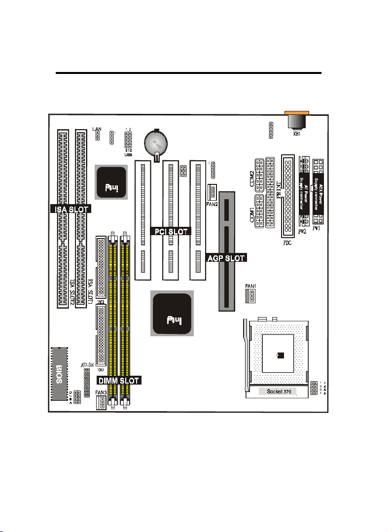
Intel 440BX PCIsetTM /440ZX PCIsetTM/VIA 693+596A
(6VIA85)/VIA693A+596B(6VIA85P) chips with I/O
subsystems.
Biggest memory capacity :
6BX85/6ZX85/6VIA85/6VIA85P is equipped with two
DIMM socket to support (16MB, 32MB, 64MB, 128MB.
256MB) 168 pin 3.3v SDRAM SPD(Special Presence Detect).
Maximum memory up to 512MB.
AGP for fast VGA solution :
AGP (Accelerator Graphic Port) will enhance & improve
display performance and Application. The bus speed is 66
MHz .
ISA & PCI Expansion Slot :
Provide two 16 bit ISA, and three 32 bit PCI slots.
PCI Bus Master IDE Controller :
(VIA Chips support UDMA66)
Comes with an on-board PCI Bus Master IDE, controller
with two connectors that supports four IDE devices in two
channels, Provides faster data transfer rate, and supports
Enhanced IDE devices such as Tape Backup and CD-ROM
devices(ATAPI). This controller supports PIO mode 3 and 4
(16.6MB/sec.), and Ultra DMA 33/66 (only 6VIA85P)
(33/66MB/Sec.), also supports ZIP100 and LS-120. BIOS
support IDE CD-ROM or SCSI bootup.
Super Multi-I/O :
Provides two high-speed UART2 compatible serial ports
(match NS16C550A compatible) and one parallel port with
SPP,EPP and ECP capabilities. UART2 can also be directed
from COM2 to the Infrared Module for wireless connections.
Two floppy drives of either 5.25" or 3.5 "(1.25MB,1.44MB
) are also supported without an external card. Supports Japa-

Chapter 2 Features / 5
nese standard "Floppy 3 mode" (3.5" 1.25MB).
CPU built-in Level 2 Cache :
128KB , 256KB or 512KB Pipeline Burst Level 2 cache
in the Socket 370 cartridge.
WOL (Wake On LAN) :
Supports system power up from LAN ring up .
IrDA Port :
Support this serial fast communication up to 115.2Kbps.
Support Ring on by modem/Alarm on :
Support System power up from Modem ring up or timer of
System. Required enabled in Ring on by modem and Alarm
on in BIOS.
To support CPU FAN On/Off and LED indicator under Sus-
pend mode.
To support CPU temperature detect and Alarm warning by
sound. ( option )

The 6BX85/6ZX85/6VIA85/6VIA85P Mainboard layout
JP7
JP8
JP6
J2

Chapter3 Installation / 7
Installation
3
Chapter 3
Jumper
Jumper Refer to page
JP4 - Real time Clock RTC clean 11
FAN1 - FAN CONN. for Socket 370 CPU 19
FAN2 - FAN CONN. for AGP 19
FAN3 - FAN CONN. for System 19
JP5 - LAN Card Wake Up 24
JP7 - CPU Front Side Bus Setting Jumper 25
JP5 - CPU Ratio Setting Jumper 25

8 / Chapter 3 Installation
Expansion Slot
Which page
168 pin DIMM Socket 13
CPU Socket370 15
AGP (Accelerator Graphic port) SLOT 17
PCI SLOT 1,2,3 -32bits PCI SLOT 17
ISA SLOT1,2 - 16bits ISA SLOT 17
Connectors Refer to page
PS2/Mouse- PS/2 Mouse port. 18
KB1 - AT Keyboard port 18
USB - USB Port 18
COM1 - COM 1 serial port 18
PRINT - Parallel port 18
COM2 - COM 2 serial port 18
FDC - FLOPPY connector 18
IDE1 - Primary IDE connector 20
IDE2 - Secondary IDE connector 20
IR - IrDA connector 21
JP6 - HDD LED 22
JP6 - Reset Switch 22
JP6 - Speaker Connector 23
JP6 - Power LED 23
JP6 - ATX Power switch 23
PW1/PW2 - ATX/AT Power Connector 23

Chapter3 Installation / 9
System Installation Setup
Before using your computer, you must finish the following steps:
1. Set jumpers on mainboard.
2. Install SDRAM module.
3. Install the Socket 370 CPU Processor.
4. Connect Ribbon Cables, Cabinet Wires, and Power supply.
5. Install Add on Cards.
6. Setup the BIOS software.
Static Electricity Precaution
Keep the mainboard and other system components in their anti-
static packaging until you are ready to install them.
Do all preparative work on a static-free surface with the main
board components facing up.
Unplug your computer when working on the inside.
Wear an Anti-static wrist strap.
Hold the system components, boards or cards by its edges only.
Be careful not to touch any of IC chips, circuitry, contacts or
connections, especially gold contacts on the mainboard.

10 / Chapter 3 Installation
Jumper Settings
Jumpers
Several hardware setting are made through the use of jumper caps to
connect jumper pins (Jxx) on the mainboard. See " Map of the
mainboard" the locationed the jumpers.
The jumper settings will be described numerically such as [----], [1-2],
[2-3] for no connection, connect pins 1 & 2, and connect pins 2 & 3
respectively. Pin 1 for our mainboard is always on top one or on the
left when holding the mainboard with the keyboard away from
yourself. "P1" is written besides pin 1 on jumper with three pins. The
jumpers will also be shown graphically such as to connect pin
1&2 and to connect 2&3. Jumpers with two pins will be shown
as for Short (on )and for Open (off).For manufacturing
simplicity it may be sharing pins from other groups. Use the diagrams
in this manual instead of following the pin layout on the board. Set-
tings with two jumper numbers require that both jumpers be moved
together. To connect the pin, simply place a plastic jumper cap over
the two pins as diagrammed.

Chapter3 Installation / 11
JP7
JP8
JP6
J2
Real Time Clock (RTC) RAM - JP4 :
The CMOS RAM is powered by the onboard button cell battery. To
clear the RTC data:
(1)Turn off your AC Power, (2) Move this jumper to "3-4Pin Clear
Data", (3) Move the jumper back to "Default", (4) Turn on your
computer, (5) Hold down <Delete > during bootup and enter BIOS
setup to re-enter user Preferences.
JP4 CMOS Clear
2-3 (default) Normal
3-4 Clear CMOS
1-4 External Battery
P1 P3P2 P4
P1 P3P2 P4
P1 P3P2 P4

12 / Chapter 3 Installation
System Memory ( DIMM Module)
This 6BX85/6ZX85/6VIA85/6VIA85P mainboard supports, two 168
pins DIMM ( Dual Inline Memory Module) of 16 MB, 32 MB, 64 MB,
128 MB ,256MB to form a memory size between 16MB to 256MB.
The DRAM can be either 45ns,50ns,or 60ns 3.3v SDRAM,and 3.3v
Enhanced Data Output (EDO) RAM.
Install memory in any or all Banks in Combination:
Bank Memory module
DIMM 1 16MB,32MB,64MB,128MB,256MB
( Bank 0-1 ) 168 pin,3.3v SDRAM / EDO RAM
DIMM 2 16MB,32MB,64MB,128MB,256MB
( Bank 2-3 ) 168 pin 3.3v,SDRAM / EDO RAM
Total System Memory(Max 512MB)
Note :
The DIMM Slot does not support any 5v EDO DIMM
module.
The DIMM Slot does not support any 5v SDRAM DIMM
module.
Memory speed setup is required through "Auto Con-
figuration" in BIOS chipset Setup of BIOS
SOFTWARE. If several speed memorious are used, You
must set Auto Configuration to low. Example If both
50ns, 60ns are used, Please set Auto configuration to
60ns.
It's allowed any DIMM module put in any DIMM slot.
It's allowed there are different capacity DIMM module
in all DIMM slot.

Chapter3 Installation / 13
DIMM Memory Installation
Insert the module (s) as shown. Because the number pins are differ-
ent on either side of the breaks,the module will only fit in the orienta-
tion as shown. SDRAM DIMM modules have different pin contact
on each side and therefore have a higher pin density.
16 Pin DIMM Socket
88 pins 60 pins 20 pins
JP7
JP8
JP6
J2

14 / Chapter 3 Installation
The Dual Inline Memory Module (DIMM) memory module must
be 3.3v Extended Data Output (EDO) DRAM or SDRAM. You can
identify the type of DIMM module by the illustration below:
168 Pin DRAM DIMM Notch Key Definitions
The notch on the DIMM module will shift between left, center, or
right to identify the type and also to prevent the wrong type to be
inserted into the DIMM slot on the Mainboard. You must ask your
retailer for Specifications before purchasing.
Four clock signals are supported on this mainboard
RFU Unbuffered
Buffered
5.0V Reserved
3.3V
DRAM Key Position Voltage Key Position

Chapter3 Installation / 15
CPU Installation
The motherboard provides a ZIF socket 370. The CPU that came
with the motherboard should have a fan attached to it to prevent
overheating . If this is not the case then purchase a fan before you
turn on your system.
To install a CPU , first turn off your system and remove its cover.
Locate the ZIF socket and open it by first pulling the lever sideways
away from the socket then upwards to a 90-degree right angle. In-
sert the CPU with the correct orientation shown . The notched cor-
ner should point towards end of the lever. Because the CPU has a
corner pin for two of the four corners, the CPU will only fit in the
orientation as shown.
Notch
JP7
JP8
JP6
J2

16 / Chapter 3 Installation
Clearance Requirements
To maintain proper airflow once the processor is installed on the
mainboard, the processor and fan heatsink require certain space
clearances. The clearance above the processor must be at least 0.3
inch. The clearance on at least 3 of 4 sides of the processor and fan
heatsink must be at least 0.2 inch. All cables (for Floppy drive,Hard
drive,CD-ROM,and so on) must be routed clear of the processor
and its airspace.
Fan Exhaust
The processor must be kept cool by using a processor with heatsink
and fan attached . The temperature of the air filled with the fan/
heatsink cannot exceed 45 OC(113 OF ) . The ambient or room tem-
perature must be below 37 OC ( 99 OF) .

Chapter3 Installation / 17
EXTERNAL CONNECTORS
Both Ribbon cable and Connectors on board are with direction signs
to avoid that user insert wrong direction. On other hand, the ribbon
cables should always be connected with the red stripe on the pin 1
of side of the connector.
JP7
JP8
JP6
J2
2PS/2 Mouse Port
1AT Keyboard
Port
3Serial
Port
COM 1,2
4Parallel
7FAN 1,2,3
Connector
9IR Port
13 Wake On LAN
6Floppy
Driver Connector
11
ATX Power
Connector
5
Universal Serial
Bus Port 1,2
12 SB-LINK
8
IDE Connector
14 CPU FSB Set-
ting Connector
10 JP6
15
CPU Ratio Set-
ting Connector

18 / Chapter 3 Installation
1. AT Keyboard port
This connector will compatible with standard at AT size (large
DIN) keyboard plugs. You may use a DIN to mini DIN adapter
on standard AT keyboards.
2. PS/2 Mouse port
This system will direct IRQ12 to PS/2 mouse.
3. Serial Port COM 1 and COM 2 port
The two serial ports can be used for pointing devices or other
serial devices. See "Onboard Serial Port" in chipset Feature Setup
of the BIOS SOFTWARE.
NOTE:
Serial {D-type 25pin (F) } must be connected to
the serial port.
4. Parallel Printer port
You can enable the parallel port and choose the IRQ through "
Onboard Parallel Port" in Chipset. Feature Setup of the BIOS
SOFTWARE.
5. Universal Serial BUS Ports 1 & 2
Two USB ports are available for connecting USB devices.
6. Floppy drive connector
This connector supports the provided floppy drive ribbon cable.
After connecting the single end to the board, connect the two
plus on the other end to the floppy drives.
This manual suits for next models
3
Table of contents
Other Acorp Motherboard manuals

Acorp
Acorp 4S651M User manual

Acorp
Acorp 7KT266A User manual

Acorp
Acorp N2PA-400 User manual

Acorp
Acorp 5ALI61 User manual

Acorp
Acorp 7NFU400 User manual

Acorp
Acorp 7KM400MN User manual

Acorp
Acorp 4845GVM User manual

Acorp
Acorp 4PX266A User manual

Acorp
Acorp 5VIA73 User manual

Acorp
Acorp 7KT400ANL User manual