Teledyne SP Devices ADQ8-8C User manual

ADQ8-8C Manual
17-2000 C 2020-09-17
1(50)
Teledyne Signal Processing Devices Sweden AB | Teknikringen 6, SE-583 30 Linköping, Sweden | www.spdevices.com
Regional sales offices | www.spdevices.com/contact
Manual ADQ8-8C
This manual describes how to get the full potential out of Teledyne SP Devices’
digitizer ADQ8-8C. The manual includes these steps:
• Set up the analog front-end
• Master the triggers
• Control the acquisition
• Manage the sampling clock
• Understanding data transfer to host PC
• Using GPIO

17-2000 C
2020-09-17 2(50)
ADQ8-8C Manual
17-2000 C 2020-09-17
2(50)
Table of content
1 INTRODUCTION ........................................................................................................... 5
1.1 ADQ8-8C Architecture ................................................................................................... 5
1.2 Fundamental design properties ..................................................................................... 5
1.2.1 Data format .................................................................................................................................. 5
1.2.2 Calibration.................................................................................................................................... 6
1.2.3 Data acquisition nomenclature .................................................................................................... 6
1.2.4 Sampling clock frequency............................................................................................................ 6
1.2.5 System clocks.............................................................................................................................. 6
1.2.6 Analog signal range ..................................................................................................................... 7
1.3 Digitizer Studio overview................................................................................................ 8
2 SETTING UP THE ANALOG FRONT-END ................................................................... 9
2.1 ADQ8-8C AFE block diagram ........................................................................................ 9
2.2 Set input impedance ...................................................................................................... 9
2.3 Set analog input range................................................................................................... 9
2.4 Set analog DC-offset.................................................................................................... 10
2.5 Adjusting the digital gain and offset ............................................................................. 10
3 SIGNAL QUALITY ENHANCEMENT........................................................................... 11
3.1 Digital Baseline Stabilizer ............................................................................................ 11
4 TRIGGER..................................................................................................................... 12
4.1 Trigger block diagram .................................................................................................. 12
4.2 Introduction .................................................................................................................. 13
4.3 Position of the trigger in the data ................................................................................. 13
4.4 Timestamp ................................................................................................................... 14
4.4.1 Timestamp definitions................................................................................................................ 14
4.4.2 Timestamp reset ........................................................................................................................ 14
4.5 Blocking triggers for synchronization ........................................................................... 16
4.5.1 Function overview...................................................................................................................... 16
4.5.2 Block triggers once .................................................................................................................... 18
4.5.3 Windowing triggers .................................................................................................................... 18
4.5.4 Gating and windowing triggers .................................................................................................. 18
4.5.5 Programming sequence for using trigger blocking .................................................................... 18
4.6 Trigger jitter.................................................................................................................. 19
4.6.1 Trigger jitter definitions .............................................................................................................. 19
4.6.2 Asynchronous triggering ............................................................................................................ 19
4.6.3 Synchronous trigger................................................................................................................... 20
4.6.4 Extended trigger resolution........................................................................................................ 20
4.7 Software trigger............................................................................................................ 20
4.8 External Trigger Inputs................................................................................................. 21
4.8.1 External trigger TRIG front panel connector .............................................................................. 21
4.8.2 External trigger SYNC connector............................................................................................... 22
4.8.3 Driving the external TRIG/SYNC signal by controlling input impedance ................................... 22
4.9 External trigger in the backplane ................................................................................. 23
4.9.1 PXIe interface ............................................................................................................................ 23
4.9.2 MTCA.4 interface....................................................................................................................... 24
4.10 Level trigger ................................................................................................................. 25
4.10.1Setting the level trigger level...................................................................................................... 26
4.10.2Level trigger and DBS................................................................................................................ 26
4.10.3Controlling noise sensitivity ....................................................................................................... 26
4.11 Internal trigger.............................................................................................................. 27

17-2000 C
2020-09-17 3(50)
ADQ8-8C Manual
17-2000 C 2020-09-17
3(50)
4.12 Trigger output............................................................................................................... 27
4.12.1Trigger output port selection ...................................................................................................... 27
4.12.2Frame sync output on SYNC connector .................................................................................... 28
4.12.3Triggering external equipment with internal trigger.................................................................... 28
4.13 Large scale integration trigger support ........................................................................ 29
4.13.1Distributing trigger...................................................................................................................... 30
4.13.2Clock reference.......................................................................................................................... 30
4.13.3High precision trigger on analog input ....................................................................................... 30
4.13.4Calibration.................................................................................................................................. 30
5 CLOCK......................................................................................................................... 32
5.1 Clock domains ............................................................................................................. 32
5.2 Flexible clock network.................................................................................................. 32
5.3 ADQ8-8C-PCIe front panel connectors........................................................................ 34
5.4 ADQ8-8C-MTCA front panel SMA connector .............................................................. 34
5.5 Internal clock reference................................................................................................ 34
5.6 External clock reference .............................................................................................. 34
5.7 Clock reference phase tuning ...................................................................................... 35
5.8 Internal clock generator ............................................................................................... 35
5.9 External clock............................................................................................................... 35
5.10 Clock reference output................................................................................................. 35
5.11 Sample skip ................................................................................................................. 35
6 GPIO ............................................................................................................................ 36
6.1 GPIO on TRIG connector............................................................................................. 36
6.2 ADQ8-8C–PXIe GPIO on SYNC connectors ............................................................... 37
6.3 ADQ8-8C–MTCA GPIO on SYNC connectors............................................................. 37
6.4 Using GPIO as a trigger............................................................................................... 37
6.5 Output .......................................................................................................................... 37
6.6 GPIO in ADQ Development Kit .................................................................................... 38
7 ACQUISITION CONTROL ........................................................................................... 39
7.1 Multi-thread notice ....................................................................................................... 39
7.2 Acquisition memory...................................................................................................... 39
7.3 Triggered streaming acquisition................................................................................... 40
7.4 Acquisition mode multi-record...................................................................................... 40
7.5 Re-arm time ................................................................................................................. 41
7.6 User scheduled data transfer mode............................................................................. 42
7.6.1 Transfer buffers ......................................................................................................................... 44
7.6.2 User’s buffers............................................................................................................................. 44
7.7 Streaming transfer mode ............................................................................................. 44
7.8 Users application software consuming data ................................................................ 44
7.9 Record header ............................................................................................................. 45
7.9.1 Metadata.................................................................................................................................... 45
7.9.2 Record Status ............................................................................................................................ 45
7.9.3 User ID....................................................................................................................................... 46
7.9.4 Serial number ............................................................................................................................ 46
7.9.5 Channel ..................................................................................................................................... 46
7.9.6 Record number .......................................................................................................................... 46
7.9.7 Data format ................................................................................................................................ 46
7.9.8 Record length ............................................................................................................................ 46
7.10 Over-range and under-range ....................................................................................... 47
8 HOST PC CONNECTION............................................................................................ 48

17-2000 C
2020-09-17 4(50)
ADQ8-8C Manual
17-2000 C 2020-09-17
4(50)
8.1 PCI Express interface .................................................................................................. 48
8.2 Using several units....................................................................................................... 48
8.2.1 Using several digitizers from a single application. ..................................................................... 48
8.2.2 Using several digitizers from a several applications. ................................................................. 48
9 REFERENCES ............................................................................................................ 49

17-2000 C
2020-09-17 5(50)
ADQ8-8C Manual
17-2000 C 2020-09-17
5(50)
1 INTRODUCTION
The purpose of this manual is to explain how the digitizer is operated. The datasheet [1] contain param-
eters for the specific versions of digitizer. References to software commands are made. In some places,
pseudo code is used for description. See [2] for details on how to use the software commands and see
[3] for general guidelines on programming the digitizer.
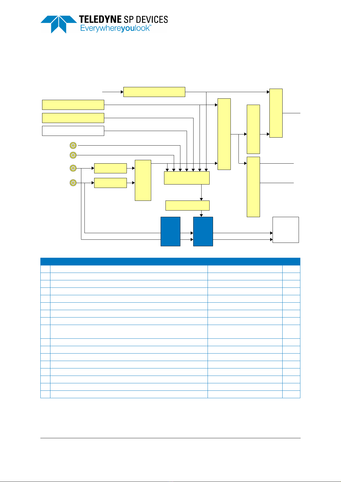
1.1 ADQ8-8C Architecture
The ADQ8-8C architecture is given in Figure 1. References to the corresponding sections with further
information are also included.
1.2 Fundamental design properties
There are some fundamental design properties that are necessary to understand before continuing.
1.2.1 Data format
The ADC components of ADQ8-8C has 10 bits resolution, while the data format inside the ADQ8-8C
and out to the host PC is 16 bits. The 16 bits from the ADCs are MSB aligned in this 16 bit data word.
Thus the 6 LSBs are zero.
#DESCRIPTION REFERENCE
a Signal conditioning analog front-end. 2
b High speed and high resolution A/D converters. 3
c Calibration of gain and offset. 2
d Teledyne SP Devices’ proprietary technology for signal quality enhancement; DBS for
baseline stability in pulse data systems.
3
e Acquisition engine that handles triggers and controls the data flow. 4, 7
f Data FIFO to buffer data before transmission to the host PC. 7
g The data transfer to the host PC is through a PCIe Gen 2 interface. 7
h Flexible clock generator. 5
i Backplane clock reference for large scale integration. 6
i Backplane clock triggers large scale integration. 4
Figure 1: ADQ8-8C architecture.
() () () () () ()
()
()
!*
%
+
,
-
."
-
+$ +*+/
()
%
%
+0
+0
+0
+0
+0
+0
+0
+0
0
1
%
-
(2)

17-2000 C
2020-09-17 6(50)
ADQ8-8C Manual
17-2000 C 2020-09-17
6(50)
The number representation is 2’s complement. The full scale maximum code is then 32 704 and the full
scale minimum code is –32 768. Overflow or underflow at any position in the signal path will saturate
the data and turn on an overflow flag. See Section 7.10 for more information on over- and under-flow.
1.2.2 Calibration
During the factory calibration procedure the analog properties are measured and parameters for a digi-
tal compensation are computed. An analog deviation in the front-end is thus compensated for by the
inverse function in the digital signal processing part.
Example 1: With the variable gain –VG option (always included with the ADQ8-8C), the user requests
a range. The closest available setting is selected and the actual range is returned to the user for being
used in the user’s algorithms, see Section 2.1.
Example 2: The full scale signal range of the ADQ is measured in production and the SetGainAndOff-
set function is used for adjusting to the correct signal range.
1.2.3 Data acquisition nomenclature
Table 1 defines some key data acquisition terms.
1.2.4 Sampling clock frequency
The ADQ8-8C is designed for the specified 1 GHz clock frequency only. A different sampling rate can
be achieved by using the sample skip function, Section 5.11.
1.2.5 System clocks
The different parts of the digitizer operate on different clock rates
The sampling of the analog signal is done on the sampling clock of the ADC (see Section 1.2.4).
The external trigger input has a trigger clock which is higher than the sample clock for high trigger time
precision (4 GHz).
The PCIe host PC connections has its own clock system.
All other interfaces operate on the data processing clock of the FPGA at 250 MHz. This clock is referred
to as the Data Clock.
Table 1: Data recording nomenclature.
PARAMETER DESCRIPTION REF
ADQ Collective name for digitizers from Teledyne SP Devices.
Analog Analog signal is the input to the digitizer. This is the signal to be digitized.
Waveform Analog signal with a distribution in time. This is digitized into a record.
Sample An analog signal level is digitized into a sample, that is a numerical value.
SYNC Physical connector on the front panel. 4.8, 6.1
Record A set of consecutive samples is called a record. An analog waveform is
digitized into a record of samples.
4
TRIG Physical connector on the front panel. 4.8, 6.1
Trigger Trigger is an event that starts acquisition of a record. 4.3
Timestamp Timestamp is a real-time value that identifies when a trigger happened.
The timestamp gives timing information for each sample.
4.4
GSPS Giga-samples per second (109). Clock frequency [Hz] and sample rate
[SPS] are both used to denote speed.
MSPS Mega-sample per second (106).
DC-offset This is an analog DC level which is added to the analog input signal inside
the digitizer to vertically move the analog signal to fit within the range of
the digitizer. This effectively doubles the ENOB for a unipolar signal.
2

17-2000 C
2020-09-17 7(50)
ADQ8-8C Manual
17-2000 C 2020-09-17
7(50)
See Section 5.1 for more details on the clock system.
1.2.6 Analog signal range
The analog signal range (ACTUAL_ANALOG_RANGE) is symmetrical around zero. The value of the
analog signal range it is depending on the gain setting. With for example a range of, 500 mVpp, the ana-
log input signal can vary from –250 mV to +250 mV and the range can be moved from [–0 mV
+500 mV] to [–500 mV +0 mV] by the DC-offset feature, Section 2.4.
The maximum digital code 2^15 represents an analog signal with a level ACTUAL_ANALOG_RANGE / 2
at the input. A specific analog signal ANALOG_LEVEL will then be represented by the following digital
code:
DIGITAL_CODE_LEVEL = ANALOG_LEVEL / ( ACTUAL_ANALOG_RANGE / 2 ) * 2^15 (1)
A specific code DIGITAL_CODE_LEVEL then represent the analog level as:
ANALOG_LEVEL = ( DIGITAL_CODE_LEVEL / 2^15 ) * ( ACTUAL_ANALOG_RANGE / 2)(2)
17-2000 C
2020-09-17 8(50)
ADQ8-8C Manual
17-2000 C 2020-09-17
8(50)
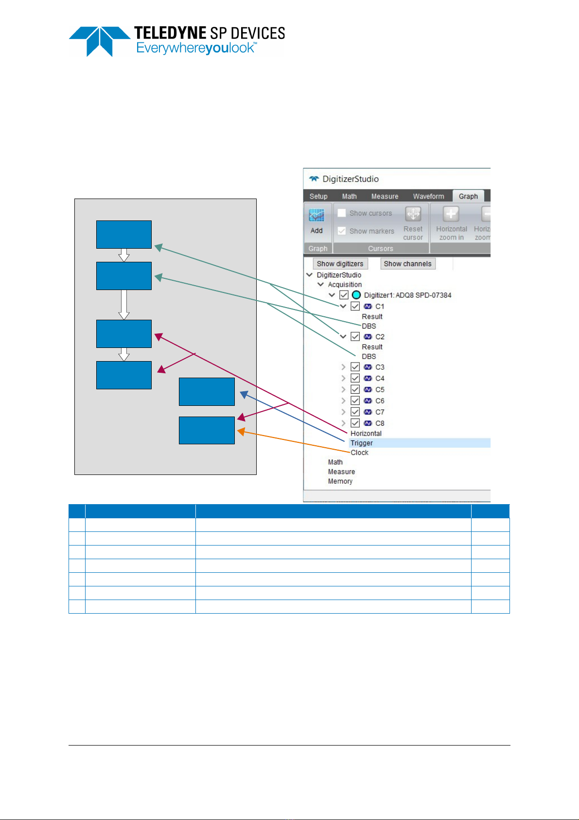
1.3 Digitizer Studio overview
The application software Digitizer Studio is an easy way to operate the ADQ8-8C. Digitizer Studio is a
graphical interface. The different blocks of the ADQ digitizer are represented by several views in Digi-
tizer Studio. These blocks are linked as in Figure 2. Digitizer Studio is documented in [5].
#BLOCK DESCRIPTION REF
a Analog front-end Setting up analog input parameters, digital signal transformation 2
b DBS Digital Baseline Stabilizer signal conditioning IP 3
c Acquisition control Setting up the recording of data 7
d Transfer to PC Data transfer methods to move the data to the PC 8
e Trigger Trigger, synchronization control 4
f Clock Timing control 5
g Digitizer Studio Digitizer Studio view [5]
Figure 2: Digitizer Studio blocks.
( )
()
()
()
()
()
()
*+
%
,"
"
!

17-2000 C
2020-09-17 9(50)
ADQ8-8C Manual
17-2000 C 2020-09-17
9(50)
2 SETTING UP THE ANALOG FRONT-END
2.1 ADQ8-8C AFE block diagram
The analog front-end setup for ADQ8-8C found in Figure 3.
2.2 Set input impedance
The analog input impedance can be set on the PXIe version to 50 or 1 M. The control is individual
per channel. The available analog signal ranges are the same for both impedance settings.
The MTCA.4 version of ADQ8-8C–VG is always 50 terminated to ground.
2.3 Set analog input range
On ADQ8-8C–VG, the input range is variable. The requested input signal range is sent to the API,
which reads available settings and return the best selection. The actual value of each range is available
for calculations according to the following:
DESIRED_ANALOG_RANGE is the requested range set into SetInputRange.
#DESCRIPTION USER COMMAND REF
a PXIe form factor: The analog input impedance can be set to 50 or 1 M
MTCA.4 form factor: input is impedance is fixed 50 to GND
SetInputImpedance 2.2
b On ADQ8-8C-VG, the gain can be set in a discrete number of steps. By
requesting a certain range, the closest available setting is activated. The
actual range that is set is returned to the user. Note that the compensation
has to be done in the software.
Changing the input range requires a settling time of 1 s.
SetInputRange 2.3
c Set a DC offset for better using the signal range when the signal is
unipolar.
Changing the DC offset requires a settling time of 1 s.
SetAdjustableBias 2.4
d The gain and offset is calibrated using a 32 MHz -1dBFS sine wave
signal. The digital compensation corrects the offset and the gain at this
frequency.
The user can access this block to set a different gain and offset. Note that
this is a digital gain and offset adjustment and not the same as selecting
analog input range in the –VG option.
SetGainAndOffset 2.5
Figure 3: AFE control.
! #$
%
)
3
)
4
3%
%
56
56
56
56
3
%
1
#$7/$
)
8

17-2000 C
2020-09-17 10(50)
ADQ8-8C Manual
17-2000 C 2020-09-17
10(50)
ACTUAL_ANALOG_RANGE is the actual calibrated range of the device returned from SetInputRange.
The maximum digital code 2^15 represents an analog signal with a level ACTUAL_ANALOG_RANGE / 2
at the input. A specific analog signal ANALOG_LEVEL will then be represented by the following digital
code:
DIGITAL_CODE_LEVEL = ANALOG_LEVEL / ( ACTUAL_ANALOG_RANGE / 2 ) * 2^15 (3)
A specific code DIGITAL_CODE_LEVEL then represent the analog level as:
ANALOG_LEVEL = ( DIGITAL_CODE_LEVEL / 2^15 ) * ( ACTUAL_ANALOG_RANGE / 2)(4)
2.4 Set analog DC-offset
A user-controlled DC-offset is available. The analog DC-offset is applied to the signal to better adopt to
the signal range of the digitizer. The analog range is by default set symmetrical around zero. If the sig-
nal is unipolar or heavily unsymmetrical, the DC-offset function can adjust the signal to an optimal verti-
cal position for the A/D converter. In this way, the full 10 bits can be used for representing the unipolar
pulse. The DC-offset is set with the command SetAdjustableBias.
The DC-offset is set in digital codes DC_OFFSET_CODE in the range [-2^15: 2^15-1], which correspond
to an analog signal level in the range:
[ –ACTUAL_ANALOG_RANGE / 2: ACTUAL_ANALOG_RANGE / 2 ]. (5)
To determine the parameter of SetAdjustableBias to get a DC-offset at the voltage level DC_OFF-
SET_ANALOG, use:
DC_OFFSET_CODE = round ( DC_OFFSET_ANALOG / ( ACTUAL_ANALOG_RANGE / 2 ) * 2^15 ) (6)
Since the digitizer has higher resolution than the intrinsic accuracy of the DC-offset generator, the
actual digital codes read out from the ADQ may differ from the expected level. For accurate baseline
measurements, the Digital Baseline Stabilizer (DBS) offers a digital correction of the baseline to an
accuracy of 22 bits, Section 3.1.
2.5 Adjusting the digital gain and offset
The digital gain and offset block is primarily intended for factory calibration but it may also be accessed
by the user, and offers an efficient way of scaling the signal to suit processing in the PC.
The default setting is the calibration parameters CAL_GAIN and CAL_OFFSET. The raw data from the A/
D converter, ADC_RAW_CODE, is corrected with the calibrated values according to:
DIGITAL_OUTPUT_CODE = ADC_RAW_CODE * CAL_GAIN – CAL_OFFSET (7)
The user can override these settings by using the software command SetGainAndOffset. The parameter
USER_GAIN and USER_OFFSET can be applied in two ways; relative to the calibrated value or relative
to the raw code.
The normal mode of operation is to apply the gain and offset settings relative to the calibrated data as
DIGITAL_OUTPUT_CODE =
ADC_RAW_CODE * CAL_GAIN * USER_GAIN – CAL_OFFSET – USER_OFFSET. (8)
By setting bit 7 in the channels parameter, the calibration data is overridden as:
DIGITAL_OUTPUT_CODE = ADC_RAW_CODE * USER_GAIN – USER_OFFSET (9)
To get the raw code, ADC_RAW_CODE, use SetGainAndOffset(128+CHANNEL,1024,0).

17-2000 C
2020-09-17 11(50)
ADQ8-8C Manual
17-2000 C 2020-09-17
11(50)
3 SIGNAL QUALITY ENHANCEMENT
3.1 Digital Baseline Stabilizer
The Digital Baseline Stabilizer, DBS, is designed for pulse data measurement where high accuracy rel-
ative a known baseline is required. The key features of DBS are:
• Tracks and compensates for baseline variations from, for example, temperature and aging.
• Suppresses pattern noise1 to 22 bits precision.
• Automatically locks the baseline to a user defined-value.
Note that DBS is off at power up. DBS has to be activated by the user’s application software. The time
when DBS is activated is important. To get a good initial estimate, DBS should be activated when there
is very little signal energy present at the input. If there is too much signal power in the initial estimate,
the convergence of DBS is slowed down.
Note that DBS is defined for systems with a baseline and distinct short pulses. DBS is not intended for
sinusoidal type of signals.
1. Pattern noise is systematic errors that may arise from the actual design of the ADC IC or the board design.
17-2000 C
2020-09-17 12(50)
ADQ8-8C Manual
17-2000 C 2020-09-17
12(50)
4TRIGGER
4.1 Trigger block diagram
#DESCRIPTION USER COMMAND REF
a Each analog input is connected to a level trigger block. SetupLevelTrigger 4.10
b Select on which channel to trigger (when using level trigger). SetupLevelTrigger 4.10
c Internal trigger generator. SetInternalTriggerPeriod 4.11
d A software trigger is available for user control. SWTrig 4.7
e External trigger input from backplane (different in PXIe and MTCA) 4.9
f External trigger input on front panel connector TRIG. 4.8.1
g External trigger input on front panel connector SYNC. 4.8.2
h Select which type of trigger to activate. SetTriggerMode
i The trigger blocking function controls the flow of triggers to the
acquisition engine.
SetupTriggerBlocking 4.5
j Select which channels to record data from. MultirecordSetChannelMask
k Acquisition engine creates a record from streaming data 7
l Records are sent to data FIFO for transfer to the host PC 7
m Activate trigger output and select source. SetupTriggerOutput 4.12
n Select trigger output connector SetupTriggerOutput 4.12
o Frame sync is a function that can group triggers. SetupFrameSync 4.12.2
p Select source for sync output SetupTriggerOutput
q Daisy chain trigger for synchronization 4.13
Figure 4: Trigger source selection and setup
'()
*#+ -
+ -
+-
+-
./"
+-
+0- +-
% &
*#
#
#
1(12
$
+-
(
'()
"//
+-
+-
+-
34
"
+-
+-
+-
// 1 "//
% &
34
+-
"& +.-
+-
34
//
17-2000 C
2020-09-17 13(50)
ADQ8-8C Manual
17-2000 C 2020-09-17
13(50)
4.2 Introduction
The digitizer can be triggered in various ways with a number of different internal and external trigger
sources. Selected events in the trigger module can also be output to trigger external equipment. The
selection of trigger source is illustrated in Figure 4.
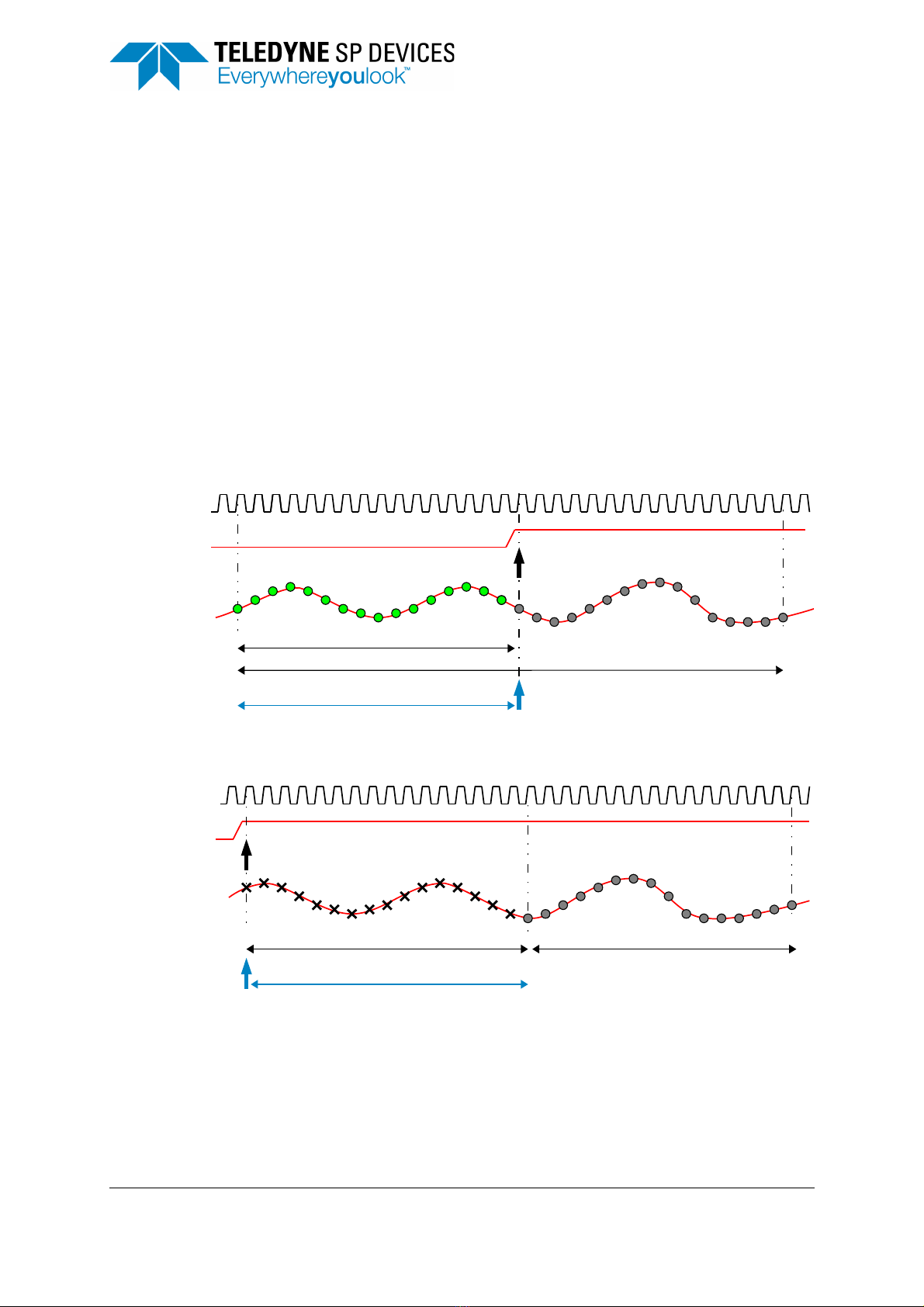
4.3 Position of the trigger in the data
The trigger position relative to the data record is controlled by the parameters pretrigger and trigger
delay.
The pretrigger buffer enables capturing data prior to the trigger event, Figure 5. Use the command Set-
PreTrigSamples to define the pretrigger.
The trigger delay postpone the start of the acquisition of the data record specified number of samples
after the trigger event, Figure 6. Use the command SetTriggerHoldOffSamples to define the trigger
delay.
The timing of the trigger is read from the record header (Section 7.9). The parameters TIME_STAMP
and RECORD_START are explained in Section 4.4.1.
Figure 5: Pretrigger timing.
Figure 6: Trigger delay timing.
#
"()
*('
'& (!'&
!!)
"

17-2000 C
2020-09-17 14(50)
ADQ8-8C Manual
17-2000 C 2020-09-17
14(50)
4.4 Timestamp
4.4.1 Timestamp definitions
The timestamp counter enables real-time measurement of a trigger event. It is used for tagging an
event, sorting events in time or comparing timing between events.
The timestamp information consist of three parts, which uniquely defines the timing:
•TIME_STAMP measures the time of the trigger event relative to other trigger events.
•RECORD_START is the time between the trigger event and the start of the record. For a pretrigger,
this is a negative value. When trigger delay is used, this is a positive value.
•SAMPLE_PERIOD is the length of a sample period. The sample period may vary with sample skip
setting and clock frequency of the digitizer.
The TIME_STAMP, RECORD_START, and SAMPLE_PERIOD are measured in the unit
TIME_BASE =25ps. See Example 3 on how to use these parameters. These parameters are available
in the record header, see Section 7.9.1.
The timestamp counter is based on the internal clock of the digitizer. The internal clock is based on the
selected clock reference. The timestamp is thus also related to the clock reference. When the clock ref-
erence is phase-locked to an external source, the timestamp counter is running synchronized with the
external source. On the other hand, if the digitizer is free running, the timestamp counter also free run-
ning. (See Section 5 for all details about the clock system of digitizer.)
The timestamp counter measures the time from a reference time point to the trigger event. The refer-
ence time point is when the counter is started or reset. See Section 4.4.2 for information on how to
reset the timestamp counter.
Example 3: Assume an ADQ8-8C sampling with a clock frequency at 1 GSPS. The pretrigger is set to
16 samples and the external trigger is used. The following parameters are returned:
TIME_STAMP = 5010
RECORD_START = –650
SAMPLE_PERIOD = 40
TIME_BASE = 25 ps
The time for the trigger was then
TRIGGER_TIME = TIME_STAMP * TIME_BASE = 125250 ps = 125.25 ns
The time for the first sample in the record is
RECORD_TIME = (TIME_STAMP + RECORD_START) * TIME_BASE = 109.000 ps = 109 ns
The time between two samples are
SAMPLE_TIME = SAMPLE_PERIOD * TIME_BASE = 1 ns
The time from the record start to the trigger is
RECORD_START * TIME_UNIT = –16.25 ns.
The number of samples between the record start and the trigger event is
( TRIGGER_TIME – RECORD_TIME ) / SAMPLE_TIME =
| RECORD_START | / SAMPLE_PERIOD = 16.25 samples
This is the expected 16 samples set in the pretrigger and 1/4 sample in subsample precision in the
external trigger.
4.4.2 Timestamp reset
When powering up a system with many boards, the timestamp counter in each board will start. But the
counters start at different times in different physical digitizers. There are four methods for resetting the
timestamp and get a common time reference in all the digitizers in the system:

17-2000 C
2020-09-17 15(50)
ADQ8-8C Manual
17-2000 C 2020-09-17
15(50)
1. The timestamp counter is reset at power-up. This methods does not, however, have absolute preci-
sion, since the timing of the power up is not defined. In a multi-board system, the timestamp will dif-
fer between the boards.
2. With a software reference reset the user has full control of the reset procedure. A reference time
point is created in the users application, which is used for aligning time-stamps in different units.
After power-up the user runs a custom timestamp reset sequence including:
• Apply a reference signal to all boards.
• Trigger a record on the reference signal.
• Read the time-stamps from the records and call this reference; TIME_STAMP_REFERENCE.
• Start the experiment and subtract the timing reference from each record as
TIME_STAMP = TIME_STAMP_OF_RECORD – TIME_STAMP_REFERENCE.
3. The third method is to apply an external trigger to reset the timestamp reset, Figure 7. This method
has the possibility to synchronize several boards to full precision of the external trigger. See Sec-
tion 4.5. The sequence of operation is:
•DisarmTimestampSync
•SetupTimestampSync
•ArmTimestampSync
The number of reset pulses are counted and the information is stored in the record header, Section
7.9. However, if there are no triggers accepted, there will be no record headers available. To verify
that there is activity going on, the number of reset pulses can also be read from a register via
GetTriggerBlockingGateCount.
4. The fourth method is to reset the timestamp with the sync signal, Figure 7. The difference between
using the external trigger and the sync is that the external trigger has the a sample resolution while
the sync timing resolution is controlled by the Data Clock in the FPGA. Note that the backplane trig-
gers in –PXIe and –MTCA formats work in the same way as the sync signal.

17-2000 C
2020-09-17 16(50)
ADQ8-8C Manual
17-2000 C 2020-09-17
16(50)
4.5 Blocking triggers for synchronization
4.5.1 Function overview
In order to synchronize the acquisition to external equipment or to other ADQ digitizers, there is a
mechanism for controlling the flow of triggers. The trigger blocking function allows the user to select
when to activate incoming triggers, Figure 8. The basic function of this block is to use the SYNC signal
to frame the trigger signals; for each period of the blocking function, a set of triggers are allowed and
and framed by the blocking event. This creates groups of triggers that belong together. The modes of
operation for trigger blocking are shown in Figure 8 (j, k, l).
To avoid that the boards start to produce a large amount of records out of sync, all trigger events can be
blocked until the triggers are released by a separate shared signal, Figure 8 (d). By combining the trig-
ger blocking and the timestamp reset, the timestamp is aligned to the start of the acquisition. The trig-
ger blocker source can be most available trigger sources, Figure 8 (a, b, c).
Note the order of the commands for activating triggers and trigger blockers, Figure 8 (e, g, h, i).
#DESCRIPTION USER COMMAND REF
a External trigger input signal on front panel connector. 4.8
b External sync input signal on front panel connector. 4.8
c Other available sources (see SetTriggerMode for a list) 4.8
d Select source for reseting timestamp. SetupTimestampSync
DisarmTimeStampSync
ArmTimeStampSync
4.4.2
e Timestamp counter value is reset at power-up of the digitizer. 4.4.2
f Reset the timestamp counter on each pulse of the selected source.
Timestamp is then measuring time relative the previous reset signal.
4.4.2
g4.4.2
h Reset the timestamp counter only on the first pulse of the selected
signal. The external signal is then a systems synchronization signal.
4.4.2
i The number of times the time stamp has been reset can be read from
a register.
GetTriggerBlockingGate
Count
4.4.2
Figure 7: Timestamp reset from external trigger.
&'
)*
)* )*
+,-./
%
+,%01
)*
)2*
)*
) *
3 )*
)*
)*

17-2000 C
2020-09-17 17(50)
ADQ8-8C Manual
17-2000 C 2020-09-17
17(50)
Figure 9 illustrates how the triggers are accepted or rejected in the window mode.
#DESCRIPTION USER COMMAND REF
a External trigger input signal on front panel connector. 4.8
b External sync input signal on front panel connector. 4.8
c Other available sources (see SetTriggerMode for a list).
d Select source for blocking triggers. SetupTriggerBlocking 4.5
e Before activating the trigger blocking any selected trigger may pass. SetupTriggerBlocking
f This signal is ignored as the trigger blocker is not armed
g Select trigger source SetTriggerMode
h Start receiving triggers. Note that triggers are still blocked. ArmTrigger
i The unblocking of triggers is armed and can be activated by (d). ArmTriggerBlocking
j Triggers are blocked until the first accepted blocker signal. SetupTriggerBlocking 4.5
k The trigger blocker can also be set up with a window function where
triggers are accepted or rejected during a user-defined window.
SetupTriggerBlocking 4.5.1
l The trigger blocker can also be set up as a gate where triggers are
accepted during a gated time set by signal (d).
SetupTriggerBlocking 4.5.1
Figure 8: Blocking and gating of triggers.
( *+,
( $$*,
-$
( *,
.
/0 12.
"3
/0 45
* ,
*,
63
*,
7"3 *,
*, *,*, *,
*,
*,

17-2000 C
2020-09-17 18(50)
ADQ8-8C Manual
17-2000 C 2020-09-17
18(50)
4.5.2 Block triggers once
The mode for blocking triggers once is illustrated in Figure 8 (j). This mode is used for starting the oper-
ation simultaneously in several units. The first time the trigger blocking signal is applied, the triggers are
allowed through. Here is the motivation for this mode:
There is no way to broadcast a software command to several units. When setting up acquisition in sev-
eral units, they will therefore be activated at different times. By using the trigger blocker, an electrical
signal to all units can activate them simultaneously. The trigger blocking signal can be external or it can
be generated internally using the bussed connections proposed in Figure 14.
4.5.3 Windowing triggers
The window mode for blocking triggers is illustrated in Figure 8 (k). The edge of the trigger blocking sig-
nal is activating a window of user-defined length which allows triggers through. There is also a mode
where triggers are blocked during the window.
The window mode can be used for two-dimensional triggering where, for example, the trigger signal is a
point trigger and a sync signal is a line trigger.
4.5.4 Gating and windowing triggers
The gate mode for blocking triggers is illustrated in Figure 8 (l). The length of the window where trig-
gers are accepted is equal to the length of the trigger blocking signal.
4.5.5 Programming sequence for using trigger blocking
The order of commands is important when programming the trigger blocking. This is because the ADQ
digitizer interact with other external equipment. This external equipment is synchronized to the digitizer
through the setup procedure.
The setup of the functions has to be aligned with the expected operation. For example, by asserting the
trigger blocking through the SetupTriggerBlocking command before setting up the acquisition, no trig-
gers are let through before the digitizer is ready.
#DESCRIPTION USER COMMAND REF
a The trigger blocker in window or gate mode allows triggers during a
certain period.
SetupTriggerBlocking 4.5.1
b Example of rejected triggers outside the window.
c Trigger within the window is accepted and a data record is recorded.
Note that the pretrigger starts before the window.
d Trigger within the window is accepted and a data record is recorded.
Note that the record extends after the window.
e Several triggers within the same window.
Figure 9: Trigger blocker examples.
'$
)*&!& +,
%!+,
%!+,
%!+,
%!+,

17-2000 C
2020-09-17 19(50)
ADQ8-8C Manual
17-2000 C 2020-09-17
19(50)
The function on the digitizer has to be activated (armed) in reverse order compared to the data flow.
This means that one stage is set up to be prepared to receive data before the preceding stage is set up
to generate data. This is especially important in streaming applications where the DRAM FIFO may
overflow if the triggering is activated before the read-out to the host PC has started.
4.6 Trigger jitter
4.6.1 Trigger jitter definitions
The triggering operation is subject to two different types of jitter, Figure 10.
1. At the trigger input is a Gaussian distributed jitter which affects the timing of the incoming trigger
signal edge. This jitter is called excess jitter and is caused by noise in the input stage. The RMS
value of this excess jitter is 25 ps.
2. The actual sampling process causes a timing uncertainty. Since the trigger is sampled with the trig-
ger clock, the time points for reading the trigger are discrete. The difference between the incoming
physical trigger signal and the digital representation of the trigger is a stochastic variable with a
rectangular distribution. The RMS value of such a process is TRIGGER_CLOCK_PERIOD/sqrt(12).
The highest resolution is achieved with an external trigger connected to the TRIG connector.
ADQ8-8C has a trigger clock at 4 GSPS, TRIGGER_CLOCK_PERIOD of 250 ps and a trigger jitter of
72 ps RMS (theoretical value), Section 4.6.4.
See Table 2 for time resolution all the external trigger sources.
4.6.2 Asynchronous triggering
If the trigger signal is not phase-locked to the reference clock it is called asynchronous. This trigger
does not have a well-determined relation to the sampling clock and will appear at various positions
within the sampling period. The time resolution of an asynchronous trigger connected to the TRIG input
is set by the Trigger Clock (4 GHz). The time resolution for other triggers is determined by the Data
Clock (250 MHz).
The asynchronous trigger will be exposed to both trigger sources from Section 4.6.1. These indepen-
dent stochastic processes are added to 72 ps. See Table 2 for time resolution of all the external trigger
sources.
There are some advantages with the asynchronous trigger:
• Any pattern noise will be reduced in repeated measurements.
• The trigger resolution of 250 ps can be used for accurate timing calculations. The TIME_STAMP
contains the information about the trigger time. See Section 4.6.4.
Figure 10: Sources of jitter on the trigger signal.
,
,
-./0/
/-1/
23%45!
6/

17-2000 C
2020-09-17 20(50)
ADQ8-8C Manual
17-2000 C 2020-09-17
20(50)
4.6.3 Synchronous trigger
A synchronous trigger is phase locked to the clock of the digitizer. The trigger source needs access to
the clock reference of the digitizer. There are three ways to achieve this synchronization:
1. Output the internal clock reference of the ADQ and send it to the trigger source, Section 5.10.
2. Use the clock reference of the trigger source as clock reference for the ADQ, Section 5.6.
3. Use the internal trigger of the ADQ and output it to trigger the external equipment, Section 4.11.
When the trigger is phase-locked to the clock reference the timing is comparable to a digital signal
which defines setup and hold time.
4.6.4 Extended trigger resolution
The basic sampling process maps the trigger to the sampling rate of the digitizer. There is also addi-
tional trigger time information available; Extended trigger resolution, Figure 11.
The Trigger Clock is operating at 4 GHz. This means that the time resolution of the trigger input TRIG is
reduced to 250 ps.
Note: The extended trigger resolution is available on triggers connected to TRIG only.
The extended trigger information is included in the timestamp information, Section 4.4.
The position of the first sample is rounded up from the trigger position. The parameter RECORD_START
tells where the trigger was. Referring to Figure 11, the RECORD_START parameter can have values in
the range –250 ps up to +500 ps. A positive value means that the first sample is after the trigger. The
given range is without pretrigger or trigger delay. With pretrigger or trigger delay, the RECORD_START
will have a larger (absolute) value.
4.7 Software trigger
The software trigger is a user command that triggers the ADQ. This is for direct user control of the
acquisition and is useful for looking at continuous signals where the timing of the trigger is not critical.
The software trigger is sent through several layers of software and the time when it arrives to the digi-
tizer cannot be predicted. However, the time when it actually arrived can be read from the time stamp in
the record header, Section 4.4.
The software trigger may also be used for time-out function. This is a way to discover faults in the
setup. When the device do not trigger for some reason within a certain time frame, a software com-
mand sequence may be sent and the data can be analyzed to find out what is wrong, Example 4.
Example 4: A time-out function using software trigger can be implemented like this:
1. Time-out occurs
Figure 11: Extended trigger resolution timing for ADQ8-8C.
,
Table of contents
Other Teledyne SP Devices Measuring Instrument manuals

Teledyne SP Devices
Teledyne SP Devices ADQ7-FWATD User manual

Teledyne SP Devices
Teledyne SP Devices ADQ7DC User manual

Teledyne SP Devices
Teledyne SP Devices ADQ7 User manual

Teledyne SP Devices
Teledyne SP Devices ADQ7 User manual

Teledyne SP Devices
Teledyne SP Devices ADQ14-FWPD User manual

Teledyne SP Devices
Teledyne SP Devices ADQ User manual


