Telequipment DM64 User manual

PAHAMQELIAJP
+ +KO?EHHKO?KLA
OPKN=CA %cUBA@I31
I=JQ=H

I
WHOHTXLSPHQWi
}
Eqfp klq mlppf\ib ql p_obbk [ii efde sliq[dbp* pl _[ob pelria \b q[hbk
klq ql qlr_e efde sliq[db q[dp, =ipl tebob mlppf\ib qeb fkpqorjbkq
pelria \b rkmirddba =J@ ptfq_eba lcc arofkd pbosf_fkd, = >HAA@AN
L=PD BKN PDA ADP EOJKP LNKRE@A@*pl [cqbo ptfq_efkd lcc
[ka \bclob qlr_efkd [kv fkqbok[i m[oqp*qeb ADP pelria \b afp_e[odba
\v qbjmlo[ofiv peloqfkd qeb [mmolmof[qb mlfkqp ql _e[ppfp* &clo
fkpq[k_b qeb ?NP _[qelab mfk[ka L@= _lkkb_qlo tebob [mmif_[\ib',
RVFLOORVFRSH
VWRUDJH WaSH GP97
FOR SERVICING AND SPARES ENQUIRIES
SEE THE INFORMATION AT START OF CHAPTER 5.
TEKTRONIX U.K.LTD.,
313 Cg_rd Rn_c,
Sntsgf_sd,
Lnmcnm, N14 6JJ
Emfk_mc.
}U(\'ICe
osi=
t/q
R
eJ
yf(1'
3fOO?
TEKTRONIX, INC.,
o._.
Bnw 500,
Bd_udqsnm,
Oqdfnm (97005)
U.S.A.
Irrtd 11 (2876)
Nnudladq 1976
{Cnoxqhfgs (1974) ax
TEKTRONIX U.K. LTD.

LX'01/
Hl_=k,,,
STORE
}I
AJD=J?A i%JPACN=PA
H
-J
·
SINGLE
REP SHOTRESET
TRIO LEVEL}}.4)]. ]
STABILITY
?K=NOA
y±±,±,,±,±±7',±,±±,cy
PNEC
HIAC
K"P
,.
POSITION J
S
PR
-
cibHK
PR
OLQH
"
.Ji PNECDB
,.
%J?DKL =Hi
oy
1
+}
yy+=o
Q
q,77
SUM..J}
=
@?
c
POSITION
q
,,+
-
=?
KcBMKJ £J%
KQP
,.
'N
EJRi77=P
Kri JKNI=H
CH2

INTRODUCTION
The OM64 is an all solid-state, dual trace, storage oscilloscope. It uses a bistable CRT to provide
a large, bright display. Stored waveforms may be viewed for up to one hour.
In the non store mode, it performs as a conventional oscilloscope.
The design of this instrument is subject to continuous development and improvement, conse-
quently this instrument may incorporate minor changes in detail from the information contained
herein, which would, in the main, affect the Components List and the reader should pay particular
attention to the notes at the beginning of chapter 5.
To minimize the risk of damaging the storage screen, the following precautions should be
observed.
Because an undeflected bright spot on the CRT screen can burn the storage target, the
BRILLlANCE control should be kept to the minimum required to produce a clear, well-defined
display. Care must be observed in the degree of writing-beam intensity used, particularly when using
slow sweep rates.
When attempting to store fast-rising or fast-falling portions of waveforms viewed at relatively
slow sweep rates, the high trace intensity required (due to the intensity difference between the
horizontal and the vertical segments) could cause storage target damage.
Avoid repeated use of the same base line position on the screen.
Do not leave a display on the CRT screen (either writing or stored) when the display is not
needed.
Do not leave STORE switches pushed in when the storage mode is not needed.
To obviate the risk of damage during transit and facilitate packaging, the owner is requested to
remove the po~er supply plug and NOT send the following items unless they are suspect, should this
Instrument be returned to TELEQUIPMENT for servicing.
Manual
Probes
Power Supply Lead
Plug Assemblies

I
CONTENTS
I
Page CHAPTER Page
I
CHAPTER
SPECIFICATION 4MAINTENANCE
&
CALIBRATION (cont.)
I
Cathode Ray Tube (CRT) 1/2 Horizontal amplifier 4/5
Cpoling 1/3 Preliminary procedure 4/2
I
Horizontal system 1/1 Probe' 4/2
Outputs, Front panel 1/2 Storage Circuit 4/6
Power Requirements 1/3 Sweep
&
Trigger 4/2
Size 1/3 Single Shot 4/5
I
Temperature limits 1/3 Vertical Amplifier
Trigger 1/2 D.C.
&
L.F. setting 4/3
Vertical System 1/1 Pulseresponse 4/5
Weight 1/3 Supply variation 4/2
I
X-V mode 4/5
General 4/1
2OPERATING INSTRUCTIONS Checks
I
Gain 4/1
Controls and Connectors Sweep Speed 4/1
Connectors, input
&
output 2/2 Mechanical 4/1
CRT
...
2/1 Accessto interior 4/1
J
Horizontal display 2/1 CRT
Sweep 2/1 Removal ... 4/1
Trig Mode 2/1 Fitting 4/1
Vertical display 2/2 Location of Pre~et controls 4/1
J
Operation 2/3
Pre-operational checks 2/3
5 COMPONENT LIST
J
3CIRCUIT DESCRIPTIONS Assemblies 5/16
Component 5/2
Attenuators 3/1 Mechanical 5/14
J
Block Diagram 3/1
CRT 3/3
EHT Supplies 3/5 6 CIRCUIT DIAGRAMS Figure
Horizontal amplifier 3/3
J
Power supplies 3/6 Attenuator 2
Sweep Block Diagram 1
Generator 3/3 Component reference
Trigger 3/2 PC Nos 110
&
112 11
J
Unblanking amplifier 3/3 PC No 111 12
Vertical amplifier 3/1 Power supply 10
Storage
9
J
Timebase ... 6
4 MAINTENANCE
&
CALIBRATION Trigger 5
Unblanking amplifier 6
Calibration 4/1 ·X· amplifier 6
J
Attenuator 4/4 ·V· amp. Input
&
Channel switching 3
Calibrator 4/6 Output
&
Trigger pre-amp. 4
CRT
...
4/3 Time/Div ...
7
J
------

CHAPTER I
SPECIFICATION
3 dB bandwidth
D.C. Coupled
A.C. Coupled
Risetime
Bandwidth (- 3 dB)
Phase error
Deflection factors
Calibrated (12 ranges 1-2-5 sequence)
Gain Xl0
Uncalibrated - with variable
Sweep generator
Sweep rates
Calibrated (23 ranges 1-2-5 sequences)
Uncalibrated (with variable)
Repetitive
1
Single Shot
J
External horizontal amplifier
3 dB bandwidth
Risetime
Deflection factors
Input impedance
Maximum input - D.C., peak A.C. or sum of
Channel 1
Channel 2 (normal or inverted)
Channels 1
&
2
Alternate
Chopped (at 150 kHz approx.)
Summed
X-V
I
xl0
:_ _ xl
D.e. - 10 MHz D.C. - 8 MHz
----
2 Hz - 10 MHz 2 Hz - 8 MHz
35 ns nominal 44 ns nominal
CH 1 is vertical input, CH2 selected via timebase switch
as horizontal input
D.C. - 1 MHz
Less than 10 at 10 kHz
10 mV - 50 V/div ± 5%
1 mV/div - 5 V/div
Complete cover between sequence and to 125 V/d iv
2 s - 100 ns/div ± 5% (without expansion)
400 ms-l00ns/div ±8% (with X5 expansion)
Complete cover between sequence and to 5 s/div
Selected by switch
D.C. - 1 MHz
350 n~
200 mV/div or 1 V/divapprox.
100
i< 1
and 30 pF approx.
400 V

Coupling
Source A.C. or D.C.
CH 1, CH2, alternate or external
Internal
Amplitude - Automatic
Trigger level 0.25 div 40Hz to 1 MHz
I
Alternate
0.25div D.C. to 1 MHz
I
1.0 div
rising to 0.5 div at 5 MHz
1 div from 1 MHz to> 10 MHz
External
Amplitude
Impedance 250mV peakto peak
100 krl parallel with 30 pF
External intensity modulation
Coupling
Amplitude, peak A.C. to Cathode
50 V maximum
20 V for perceptible modulation at average brilliance
10 nF and 10 krl
1 hour
Manual or automatic at end of sweep
0.25 s. approx.
Time constant
Store Mode
Erasure
Erase time
Writing rate
Enhance off
on
Variable enhancement
25 div/ms
250 div/ms
25 - 250 div/ms
Calibrator, peak to peak
Accuracy
Sweep sawtooth
Coupling
Amplitude peak to peak
Minimum load
Gate out
Coupling
Amplitude, peak to peak
500 mV square wave at supply frequency
2%
D.C.
10 V approx.
47 krl
D.C.
500 mV approx.

100 - 125 V in 5 V steps
200 - 250 V in 10 V steps
48 - 400 Hz
100 VA approx.
Frequency
Consumption
Height
Width
Depth
24 cm
21 cm
37
cm
Operating
Non-operati ng - 5 to +40oC approx.
-25
to +70oC approx.

CHAPTER 2
OPERATING INSTRUCTIONS
2.1 FUNCTION OF CONTROLS
AND CONNECTORS
Controls are situated on the front panel except
when specified
2.1.1 CRT
BRILLIANCE
FOCUS
ASTIG/
POWER ON·OFF
BEAM LOCATE
ERASE
MANUAL
varies the intensity of the display.
controls the definition of the display.
is used in conjunction with FOCUS
for best overall definition.
when pressed a spot will appear in the
non-store area 2 mm approx to the
left of the start of the trace. This
facility is provided for vertically posi·
tioning the trace without storing it.
when pushed in the trace can be
stored for up to one hour.
Note: Change of mode causes the
Store to be cleared and the stored
traces destroyed.
when pushed in, the writing speed is
increased.
controls the writing speed up to
X10
approx.
Note: This facility reduces the
contrast and hence storage time.
this facility is provided for storing a
recurrent signal at high writing speeds.
when depressed, the stored trace is
removed.
when switched to AUTO, the stored
trace is automatically erased at the
end of each sweep and the timebase
armed for the next input signal.
TRACE ROTATION situated on the rear panel. Rotates
the trace(s) about the horizontal axis
of the CRT and used to align the
trace(s) with the horizontal graticule
divisions.
2.1.2 HORIZONTAL DISPLAY
POSITION varies the location of the trace(s) in
the horizontal axis, when not in the
X·Y mode.
acts as a more sensitive position
control as well as the X5 horizontal
gain switch. When pulled out in the
X5 position, all sweep speed calibra-
tions must be divided by 5. In the
X-V mode, FINE inoperative, X5 gain
operative.
2.1.3 SWEEP
TIME/DIV
2.1.4
TRIG
MODE
TV F 'md TV L
controls the speed of the main sweep.
The sweep rates indicated are only
valid if VAR IABLE is fully clockwise
and FINE position is pushed in for
X1 gain. If FINE position is pulled
out and VAR IABLE is at CAL. the
calibrations should be divided by a
factor of 5 to ascertai n the sweep
speed.
enables speeds between that indicated
by TIME/DIV and the next lower
speed to be selected. The control also
selects X-V operation when the knob
is pushed in.
selects that point on the signal wave-
form at which the sweep starts. In the
AUTO position. ref 2.1.4 below, the
trigger oscillates recurrently at a low
repetition rate in the absence of a
triggering signal; when a suitable
signal is applied. the circuit is auto-
matically triggered at the mean level
of the input waveform.
controls the sensitivity of the sweep
generator; turned fully anti-clockwise
prevents the sweep from running,
while fully clockwise causes the
sweep to free ru n.
assist in viewing or photographing a
non-recurrent signal. If a recurrent
signal is applied to the oscilloscope.
in the SINGLE-SHOT mode, the
sweep will run once each time RESET
is pressed. when
not
in the X-V mode.
When a recurring signal is applied. the
timebase should be locked by using
STABILITY and LEVEL.
facilitates triggering from TV field
(frame) or line pulses; the LEVE L
control may require adjustment for
best results. Polarity relates to the
sense of video modulation.
should be depressed for synchroniza·
tion from high·frequency signals.
LEVE L can be adjusted for a locked
sweep.

provide triggering from the positive
or negative-going slope of a wave-
form.
obtained by releasing DC and AC
buttons.
enable the sweep to be triggered
either internally from the vertical
amplifier or externally.
relate to the coupling of the trigger
circuit. For very low input frequency
DC should be selected.
2.1.5 VERTICAL DISPLAY
OFF-ON release of these buttons,switches off
the channel concerned. If both
channels are switched off, a straight
line trace results which cannot be
shifted by the POSITION controls,
except when in the X-V mode.
selects triggering from either or both
channels. When alternately triggering
from both channels both INT TRIG
buttons should be released; the
displays should be partially super-
imposed.
provide three display modes for the
vertical channels.
In the CHOP mode, the channels are
alternately switched on and off at a
frequency of about 150 kHZ; this
mode is suitable at the lower sweep
speeds. In the AL T mode, each
channel is alternately displayed for
the duration of a sweep; this
mode is preferable at higher sweep
speeds.
In the SUM mode, the display is the
addition of the individual signals.
CHl POSITION is used to shift the
trace, CH2 POSITION is a Fine shift
in the SUM mode.
If INVERT is depressed,the resultant
display is the difference between the
two input signals.
displaces each trace in the vertical
direction except when both channels
are off.
In the X-V mode irrespective of
button settings CH1 provides a verti-
cal shift and CH2 a horizontal shift.
the setting of this button determines
whether the CH2 signal isdisplayed in
the same polarity asthe input signal
or inverted. The inverted setting is
used to display the difference
between two signals in the SUM mode.
provides twelve steps of attenuation
of each channel's input signal.
Calibrated sensitivities are only valid
when VARIABLE is fully clockwise.
enables all deflection sensitivities
between that selectedby the VOLTS/
DIV switch and the next below to be
covered. The control must be fully
clockwise for acalibrated display; for
Xl0 gain the knob should be pushed
in.
selects the input signal coupling. In
the DC position, the signal from the
INPUT connector is coupled directly
to the attenuator.
In the AC position a capacitor is
inserted in series.
In the GND position the input to the
attenuator is grounded and socket
disconnected; this position enables
the 0 V D.C. level of a trace to be
ascertained.
2.1.6 INPUT AND OUTPUT CONNECTORS
1. INPUTS
BNC
2. OUTPUTS
CAL
connectors are linked to the vertical
channel attenuators via the DC-GND-
AC switch described above.
there is a BNC connector in the
sweep section of the front-panel.
This enableseither external triggering
signals to be applied, or in the EXT
condition of the VARIABLE speedit
provides the EXT X input. The con-
nector is D.C. coupled to both trigger
and horizontal amplifier circuits. An
external blocking capacitor may be re-
quired to removethe D.C.component.
Input resistanceis 100 kU
A X5 amplification of the horizontal
display is obtained by pulling out
FINE position. If a dual-trace display
is required on EXT X, the vertical
display mode must be set to CHOP,
the AL T and SUM modeswill provide
only one trace.
at thE; rear of the instrument and
connected via an isolating capacitor
to the CRT cathode. A negative-going
signal is thus necessary to intensify
the trace while a positive-going signal
will blank it.
socket provides a waveform for
checking the calibration of the vertical
channels.
The repetition rate is at supply
frequency.
provides a fast-edged positive-going
rectangular pulse lasting for the
duration of the sweep.
The gate out signal or 0.5 V peak to
peak 1 kHz squarewave is used for
calibrating probes asfollows.
1. Connect the probe to INPUT 1.
2. Set VOLTS/DIV to
.1 (X10),
10 mV (Xl001.
3. Turn VARIABLE fUlly clockwise.

~
,
,
,
I
I
I
SAWTOOTH
ill
4. Set TIME/DIV to 1 ms.
5. Connect probe tip to the GATE
OUT.
6. Adjust the probe trimmer for a
square corner on the leading edge
of the display as follows:
In the HZ1 B probe, a screwdriver
adjustment is provided through a hole
in the probe body.
The GE81 000 is calibrated asfollows:
1. Slacken the narrower of the two
knurled rings at the BNC connec-
tor end of the probe cable.
2. Rotate the adjacent broader ring
until a square corner is obtained.
3. Tighten the narrow ring without
disturbing the broad ring.
If a 1kHz squarewave is used, the
amplitude should be about 500 mV
and a few cycles of the waveform
should be displayed. The above
calibration procedure should be
followed with X10 probe tip applied
to the squarewave generator output.
The compensation should be checked
if the probe is transferred to INPUT 2.
provides a positive-going ramp wave-
form when the sweep is running. A
recurring sawtooth is produced when
the STABI L1TY is fully clockwise for
the sweep generator to free-run. The
resistance of an applied load should
exceed 47 k,Q to avoid loading the
sweep generator.
th is is connected to the chassis of the
instrument.
2.2.1 Before connecting the instrument to the supply, check
that the rear voltage-selector plug is indicating the local
supply voltage or the nearest value to it. Check also that the
fuse fitted is 1 A for 100-125 V operation or 500 mA for
200-250 V.
NOTE:-
The 3-core supply lead is alternatively colour coded
as follows:
Brown
Black
Earth
(Chassis)
Green/Yellow
Green
Blue
White
1. CRT
BRILLIANCE
FOCUS
ASTIG
STORAGE
TRACE ROTATION
Mid Position
Central
Fully anti-clockwise
Off
As set
2. HORIZONTAL DISPLAY
POSI TI ON Central
FINE Central and pushed in
3. SWEEP
STABILITY
TIME/DIV
VARIABLE
LEVEL
TRIG MODE
SINGLE SHOT
Fully clockwise
5
ms
Fully clockwise
Any position
A 11buttons out
REP.
4. VERTICAL DISPLAY CH1 & CH2
OFF-ON ON
INT TRIG 1
CHOP AL T-SUM CHOP
POSITION Central
INVERT-NORMAL NORMAL
VOL TS/DIV 0.2 V
VARIABLE Fully clockwise
DC-GND-AC GND
1. Plug into the supply and switch on by the ASTIG. LUM.
2. Allow a few minutes for warm up then adjust CRT and
POSITION controls for a two-trace display.
3. Adjust TRACE ROTATION if necessary to make the
traces horizontal.
4. Apply the supply frequency squarewave from the CAL
500 mV peak to peak socket to both INPUT connectors
via co axial leads and switch both DC-GND AC to DC.
5. Rotate STABILITY anti-clockwise to lock display.
6. If the supply frequency is 50 Hz, 2.5 cycles of the
calibrator waveform will be displayed. each display being
2.5 div in amplitude.

CHAPTER 3
CIRCUIT DESCRIPTIONS
3.1.1 This chapter wi
11
assist the reader to comprehend the
circuitry of the OM64. By referring to the Block Oiagram
reference Figure 1 the reader will seethe interfaces of the
various circuits and signal paths, which will be dealt with in
detaiI later.
3.1.2 The signal is fed via the Attenuator to the Vertical Am-
plifier. Its description covers the function of the 'Y' input
pre-amplifiersand Output amplifier, Channelswitching multi-
vibrator and trigger pre-amplifier. The output isfed to the 'Y'
plates of the CRT with a portion of it beingfed to the trigger
network.
3.1.3 The Trigger circuit provides pulsesof suitable amplitude
and polarity to trigger the timebase from internally or ex-
ternally derived waveforms.
3.1.4 The Timebase description deals with the AL T pulse and
Sweep generators, Gating and Hold-off bistables. This stage
determines the start and finish of eachsweepand generatesa
sawtooth waveform for the horizontal amplifier.
3.1.5 The Horizontal amplifier description coversthe
'X'
output,
which amplifies the sawtooth waveform or an external
'X'
signal and appliesit in push-pull to the
'X'
platesof the CRT.
3.1.6 The Unblanking amplifier description coversthe Chop and
Sweep retrace blanking amplifiers. The output being fed to
the CRT g2 electrode.
3.1.7 The Calibrator and E.H.T. are included with the descrip-
tion on the Power supplies, the function of the former is to
provide a calibrated peak to peak squarewaveat power·line
frequency for the purpose of checking the vertical amplifier
and timebase calibration.
3.1.8 The CRT description covers the store and non store
switching, manual and auto erase generators, enhance
generator and collimation correction for the storagesection
of the CRT Also included is a brief description of the
mannerin which the CRT actually storesinformation.
The signals to be observedare connected to the instrument
via BNC sockets and switch S901, referenceFigure 2. Two
identical attenuators each comprising four frequency-
compensated resistive dividers with ratios of 100:1, 10:1,
5:1 and 2:1. Theseare switched singly or in tandem; C902,
C905, C908 and C912 serveto standardize the input time
constants; C904, C907, C911 and C914 compensate the
respective dividers.
3.3 VERTICAL AMPLIFIER
('Y'-AMPLI FIER)
The circuits of channel 1 (CH1) and channel 2 (CH2) are
identical with zenerdiodes 0604, 0611 providing stabilized
positive and negative voltages and diodes 0607, 0608 the
shift voltages CH1 is described below reference Figure 3.
Where references are made to CH2, CH2 will be quoted.
3.3.1 The output from the attenuator is fed to the gate of
TR601 via a protection circuit C601, C602, R601, R602a,
R602b, and R603 which prevents excessive voltage
damagingthe input FET.
3.3.2 TR601 and TR602 form a paraphaseamplifier with their
sources long-tailed through TR628. R624 provides variable
gain control. Compensation is provided by R625 for trace
movement causedby varying R624. R622 compensatesfor
supply voltagevariation in conjunction with R626, R630,
R632 and 0604. Neutralization is effected by C604.
3.3.3 The output from the FET input stageis taken via emitter
followers TR603 and TR604 to a gain stage TR605 and
TR606. In the emitter circuit R617 setsthe X1 channelgain
and R618 the X10. The collector outputs are connected to
the switching stage,TR609 and TR611, via emitter followers,
TR607 and TR608, which provide in push-pull the channel
trigger signal. The Miller capacities of the above gain stage
areneutralized by C603 and C609.
In CH2 the emitter followers TR624 and TR625 provide the
horizontal signalin the X-V mode.
3.3.4 TR609 and TR611 form a long-tailed pair with C606 and
R614 providing H.F. compensation. Their output feeds a
shunt feedback amplifier TR612 and TR613. The feedback
resistors are split into pairs, R644, R650 and R658 R661;
with H.F. compensation being provided by C621, R656,
C619, R655, connected between the junctions of the above
pairs of resistors.
3.3.5 The output from TR612, TR613 is fed to the emitter
input of the output stage,TR752 and TR753, which drives
the 'Y' platesof the CRT Fig.8.
A portion of the output is taken via a balanceddivider, R771,
R773 and R772, R774 to switch, S751,which switcheseither
the above portion of the-signalor the channelsignalfrom the
emitter followers, TR607 and TR608, to a long-tailed pair
TR755, TR757, which drive the Trigger circuit.
3.3.6 The CH2 output from TR624. TR625 also drives a
separate long-tailed pair. TR754, TR756 which acts as a
horizontal pre-amplifier in the X-Y mode. The X-V gainsare
equalized with R787. The outputs from TR754, TR756
collectors drive the diode switching matrix in the horizontal
output amplifier.
3.3.7 Channel switching is carried out by TR614 and TR615,
which act asa bistable in the ALT mode and a free-running
multivibrator in the CHOP mode the current being provided
via a long-tail TR616.

3.3.8 In the AL T mode a negative-goingpulse coinciding with
the start of the sweep flyback is fed, via 0606 or 0609, to
the above bistable causing it to switch. When TR614 is
conducting, it passescurrent from the switching stage,TR609
and TR611, allowing the CH1signalto passto the shunt feed-
back amplifier, TR612 and TR613. At the sametime TR615
is off, its collector rises to 16 V approximately taking the
emitters of CH2 switching stage,TR626 and TR627 with it
and so cutting off the current. Oiodes 0610 and 0612
prevent the base-emitterjunctions from breaking down in the
reversecondition.
3.3.9 In the CHOP mode, R664 and R648 are returned to H.T.
via R639 and R649, forming an astable multi vibrator. The
frequency is mainly determined by R664, R648, C613, C622,
R647, R663, R639 and R649.
3.3.10 In the SUM mode, the current supplied via TR616 is
switched off, so both TR614 and TR615 are non-conducting.
Both switching stages,TR609, TR611 and TR626, TR627
are required to be on, so extra current is bled from the 115 V
line via R637 and R638. Current flows through the switching
stages,via R646 and R662 through R673 to earth. Hence
these signals are added at the basesof TR612 and TR613.
CH2 signal can be inverted by switch, S604, to provide
addition or subtraction of the two signals.Also in the SUM
mode, CHl POSITION becomesa coarseshift control. CH2
POSITION being the very fine shift control.
3.3.11 The table below shows the state of the switched
components for all switch combinations; followed by a
resumeon the part of circuit activated.
Condition A denotes R637, R638 connected to
+
110 V.
Condition B denotesTR616 conducting.
Condition C denotes R673 connected to junction R646/R662.
ALTernate CHOP SUM
x-y
I
CHl CH2 A B C ABCA B C A B C
ON OFF NO YES NO NO YES NO NO YES NO NO NO NO
OFF ON NO YES NO NO YES NO NO YES NO NO NO NO
ON ON NO YES NO NO YES NO YES NO YES NOiNO,NO
OFF OFF NO YES NO NO YES NO NO YES NO N°iNOINO
1. CHl On, CH2 Off.
TR614, TR609 and TR611 are conducting, this feeds the
output of TR609 and TR611 to the basesof TR612 and
TR613; TR626 and TR627 being reversed biased by the
potential at TR615 collector.
TR615, TR626 and TR627 are conducting,so only the output
of TR626 and TR627 may passto the basesof TR612 and
TR613; TR609 and TR611 being reversed biased by the
potential at TR614 collector.
TR614 and TR615 are connected to form a bistable circuit.
At the end of each sweep,a negative-goingpulse appearsat
the junction 0606/0609 which reversesthe state of the
bistable. Hence TR614 and TR615 conduct alternately and
allow the outputs of CHl and CH2 alternately to reachthe
basesof TR612 and TR613.
-1
R648 and R664 are returned to H.T. via R639 and R649 to
form an astable multivibrator, which free runs at 150 kHz
approx. Thus the outputs of CHl and CH2 are successively
switched into TR612 and TR613 at 150 kHz. At each
transition a pulse is fed from the emitters of TR614 and
TR615 via C642 to the unblanking amplifier Fig.6, which
blanks the CRT beam and thus provides automatic transient
blanking in the chopped mode.
The tail of the multivibrator and R633 are disconnected;
TR614 and TR615 are non-conducting; R673 is connected
to ground providing a current path for both channels
simultaneously; TR609, TR611, TR626 and TR627 are
conducting; extra current being fed to their collectors, via
R637 and R638 from the
+
110 V line, to maintain correct
conditions. CHl and CH2 may be used as a summing or
differential (with INVERT pressed)amplifier. In this mode,
the CHl POSITION control provides a coarseshift, and CH2
POSITION control provides a very fine shift control
(reference3.3.10).
TR614 and TR615 are non conducting, preventing outputs
from either CH1 or CH2 from reaching TR612 and TR613.
When the X-Y switch is selected,the circuit is connected for
X-Y operation asfollows, regardlessof any vertical amplifier
mode switching. R641 is returned to ground, ensuring CH1
signal is connected to TR612 and TR613; TR626 and TR627
are biased off, TR616 is non-conducting and the junction
R646/R662 is returned to HT.
The basesof trigger input amplifiers TR2 and TR3, reference
Figure 5, are fed with internal or external trigger signalsvia
switch, S4,whi'chselectsthe sourcefrom either the collectors
of TR753 and TR754 in the vertical amplifier or TRl the
external trigger amplifier. S2selectsthe polarity of the signal
on which the triggering occurs.
3.4.1 Whenswitched in by S3aorS3b, R15,the LEVEL control
varies the basepotentials of TR2 and TR3 in antiphase.This
alters the quiescentvoltage on the baseof TR4 and O.C. level
of signalrequired to trip TR4 and TR5.
3.4.2 When S3a and S3b are open in the AUTO position, feed-
back is applied from TR4 collector via R27 and R9 to TR2
baseand from TR5 collector via R26 and R23 to TR3 base.
This feedback causesTR2, TR3, TR4 andTR5 to oscillate,in
the absenceof a trigger input, at a low frequency primarily
determined by Cll, R26 and R27. Input signalsare A.C.
coupled only and override the above oscillation, causingthe
circuit to lock to the input frequency. The trigger sensitivity
is set by R34, this adjusts the hysteresisof TR4 and TR5.
R17 is setto provide symmetrical operation of TR2 and TR3.
3.4.3 When Sla and b are in the NORMAL position, TR4
and TR5 form a Schmitt trigger. The constant amplitude
rectangular-wave output at the collector of TR5 is

differentiated by C15 and R38. The resulting bidirectional
pulses are applied to the series clipper 01, which provides
the collector of TR68 in the sweep circuit with negative-
going trigger pulses.
In the TV positions of Sla and b, R25 is disconnected from
the emitter of TR4; TR4 converts into a sync separator with
C12 being switched across R31. TR5 changes into an inverter
with decoupling capacitor C16 being switched across the
emitter resistors R36, R25 and R34. In the TV F position of
Sl a, the differentiating time-constant of C15 and R38 is
increased by the addition of R39.
3.4.4 With Slc set to HF, R32 is added in series with R34
across C14; this converts TR4 and TR5 into a free-running
oscillator whose frequency is adjusted, by R15 the LEVEL
control, to synchronise with the H.F. trigger input.
The sweep genArator, reference Figure 6, consists of a Miller
integrator TR71 and emitter follower TR72; and also
bistables, a gating bistable TR66, TR68 and hold-off
bistable TR73, TR74, connected between the Miller output
and input.
3.5.1 Initially, for an incoming trigger pulse to fire the sweep
the following conditions apply:-
Diodes 067, 068 and TR69 are conducting and clamp the
drain of TR71 at
+
2.5 V approx. The hold-off bistable is
held with TR73 off, TR74 on and the gating bistable with
TR66 on, TR68 off.
3.5.2 A negative-going trigger pulse causes TR66 to switch off,
TR68 on, and 066 to conduct. Hence current flowing through
R84 diverts from 067, 068 to 066. This open circuits 067,
068 and releases the gate of TR71. TR71 drain starts to rise,
due to Miller action, taking TR72 base and emitter with it
and cutting off TR69. This rising sawtooth voltage passes
through 071 until eventually TR73 base becomes sufficiently
positive to switch the bistable over. Hence TR74 switches off,
TR73 on and the negative voltage step at TR73 collector
causes TR68 to switch off and TR66 on. TR68 collector
goes positive, switching 066 off, 067 and 068 on; starting
the flyback.
3.5.3 Current flows through R84, 067 and 068 into the timing
capacitor Ctto commence flyback. When TR72 emitter has
fallen sufficiently taking TR69 emitter with it then TR69
conducts and clamps Ctat the initial start potential. This
potential is determined by the resistor ratios R85, R86, R94
and R95.
3.5.4 During the flyback period, 071 is off due to the charge
on the hold off capacitor Ch' This charge leaks away through
R104, R105, R106, R107 and Rl12 until eventually TR73
switches off, TR74 on; the initial conditions (3.5.1 above)
are restored.
3.5.5 When the sweep is switched to single-shot mode, TR73
base is prevented from switching at the end of the flyback
and clamped by diode 072. The bistable is switched over by
pressing RESET, this applies a negative-going pulse to TR73
base and causes the collector current to switch off and TR74
to conduct. The circuit is then ready for the next incoming
trigger pulse to fire the sweep.
3.6 HORIZONTAL AMPLIFIER
(X-AMPLIFIER)
The horizontal amplifier reference Figure 6, consists of a
pre-amplifier TR76, followed by a cascode connected long·
tailed pair output stage, TRn, TR78, TR79 and TR81.
3.6.1 The pre'amplifier TR76 is a shunt feedback stage in
which the sweep and shift voltages are mixed via Rl03,
R121 on its base. In the EXT X position;TRl is connected in
place of a sweep signal, which converts the high impedance
external input into a low impedance suitable for mixing with
the shift voltage at TR76 base. The TR76 collector output is
fed to the base of TR78 via 076. TR78 and TR79 form the
bottom half of a cascode amplifier, their collectors driving
the emitters of TRn and TR81; tail current being supplied
via TR82.
3.6.2 Gain control is provided in the Xl condition by R132,
in the X5 position by R131. The output from TRn and
TR81 collectors driving the CRT
X
plates.
3.6.3 In the sweep and EXT X positions 076 and 081 are
conducting; 077 and 082 are not conducting, the signal
being fed to the base of TR78 with 075 and 079 not
conducting. 074 and 078 are conducting shorting the
collectors of the X-V pre'amplifier TR751 and TR752.
3.6.4 In the X-V mode 074 and 078 are not conducting, 075
and 079 are conducting allowing the push pull output from
CH2 to be fed to the bases of TR78 and TR79. Also 076 and
081 are not conducting; 077 and 082 are conducting
shorting out the signal on TR76 collector.
The amplifiers for unblanking comprise TR65, TR67 and for
chopped blanking TR62 and TR64, reference Figure 6.
3.7.1 In the absence of a sweep TR66 conducts, causing current
to flow through TR65 making the TR65 collector, the TR67
emitter and the CRT Mod Plate electrode negative with
respect to the CRT A 1 electrode so blanking the trace.
3.7.2 When the sweep starts TR66 switches off; TR65 current
ceases; hence its collector goes to h.t. causing TR67 emitter
and CRT Mod Plate to follow. The potentials of A1and Mod
Plate electrodes are equalized so unblanking the trace.
3.7.3 Chopped blanking pulses are fed from the vertical
amplifier via C642 to the cascode circuit TR62 and TR64,
which amplifies the pulse. The collector of TR64 falls;
allowing 064 to conduct and pass blanking pulses, via TR67
to the CRT Mod Plate electrode to blank the trace.
The CRT is of the direct viewing bistable storage type and
contains special storage electrodes additional to a
conventional CRT To make the circuitry comprehensible
two figures are included in this manual. Figure 8 shows the
conventional mode circuit. Figure 9 the storage.

3.8.1 The storage circuit provides the voltage levels necessary to
operate the flood guns, collimation electrodes, target back-
plate, and erase generators. Additional circuitry includes the
enhance generator, which permits faster single sweeps to be
stored and the integrate switch which permits a stored image
of a number of repetitive sweeps, each of which are too fast
to store alone as a single sweep.
Fig. 1 a block diagram includes the storage circuit.
3.8.2 Storage Basic Operating Principles
The storage target backplate (STB) collects the secondary
electrons emitted by the insulator surface, when the insulator
is bombarded with high energy electrons from the writing gun.
This stored positive charge on the insulator is then used to
control the flow of flood gun electrons to a phosphor screen,
in order to produce a visual image.
3.8.3 The flood guns provide low energy electrons directed in a
large cone towards the screen, the collimation electrodes
shape the electron beam to provide uniform coverage of the
STB.
3.8.4 The operating level of the tube, that is the storage or non-
storage mode, is determined by the potential difference
between the STB and the flood gun cathodes.
3.8.5 In the storage mode, the following states are required to
exist in sequence.
1. Ready to write. The insulator surface of the STB tends to
discharge down towards the flood gun cathodes, such that
the flood gun landing energy is not sufficient to illuminate
the phosphor in the target.
The target is now ready to write.
2. Writing. The storage target is scanned by high energy
electrons from the writing cathode. These electrons cause
secondary emission to occur over the scanned area and the
bombarded surface charges sufficiently positive to switch
over to a higher voltage stable state and remains in this
state after the writing gun excitation is removed.
3. Viewing. In this written state, the potential difference
between the flood gun cathodes and the STB has
increased due to the positive charge on the insulator. The
flood gun electrons now penetrate the written area and
illuminate the phosphor. This visual display will persist as
long as the flood beam is allowed to continue to land on
the insulator surface.
At high sweep rates, the writing beam energy is not
sufficient to cause the insulator to switch to the upper
voltage stable state, so when flood gun electrons land on
the target they discharge the insu lator down to the flood
gun cathode potential.
Hence, storage is a function of writing speed.
4. Erasure. When the stored display is no longer required, a
positive pulse is applied to raise the whole STB voltage
above the writing threshold, so that the whole area is
written with flood gun electrons The pulse then goes
negative and as the voltage gradually returns towards zero,
the target is charged towards the ready to write threshold
and the whole procedure can be repeated.

3.8.6 Circuit Description:
The circuit, reference Figure 9, comprises three triggered
monostable pulse generators; enhance TR100l, TR1002,
manual erase TR1003, TR1004 and auto erase TR1007,
TR1009. The outputs from these circuits are connected, via
the erase amplifier TR1005, TR1006, to the CRT STB
electrode. Additionally O.C. supplies are provided for the
collimation electrodes CEl to CE5.
3.8.7 In the NORMAL (non-store) condition of the CRT, the
base of TR1005 is connected to a fixed potential. TR1005,
TR1006 are connected as a single stage shunt feedback
amplifier; the O.C. output level sets the STB potential at
approximately 75 V.
3.8.8 When switched to STORE mode, the base of TR1005 is
connected to a resistive mixing circuit comprising, the O.C.
level adjustment Rl026, via Rl028, the erase generator out-
put from TR 1004 via R1029 and the enhance generator out-
put from TR1002 via Rl031. The STB electrode resides at a
potential of approximately 150 V.
Note:
These potentials will vary from instrument to
instrument.
3.8.9 The ENHANCE and AUTO ERASE monostables are
triggered by a pulse from the sweep generator that occurs at
the start of the flyback period. This pulse is shaped by
TR1000 and applied via Cl00l and Cl014, to the respective
monostables.
The MANUAL ERASE is applied via S1004a. A negative
pulse is applied to the base of TR1003 causing it to switch
off, TR1004 to switch on and bottom. The circuit will switch
back after a period determined approximately by Cl007 ana
Rl017; the collector of TR1004 will then rise until it is
clamped by 01007. When TR1004 switches on, it also
discharges Cl008. Hence at the end of the pulse period
Cl008 will charge towards -100 V line until clamped by
01008 at -14 V.
3.8.10 The waveform at TR1005 base is the sum of the O.C.
level, a negative-going rectangular pulse of approximately
14 V amplitude from the TR1004 collector followed by an
exponential decay back to -14 V approximately from the
negative side of Cl008.
3.8.11 This signal is inverted and amplified by the shunt feed-
back stage TR1005, TR1006 and applied to the STB
electrode of the CRT. At the same time, the emitter of
TR1006 drives the bootstrap emitter follower TR1008 via
the zener diode 01014. The signal voltage passes through
Cl013 cutting off 01009 so disconnecting the +300 V line.
The collector of TR1006 rises due to bootstrap action taking
the collimation electrodes CE4, CE5 positive. This is done to
maintain correct collimation of the flood beam during the
erase period.
3.8.12 The AUTO ERASE generator is triggered by a negative
pulse occurring at the start of the sweep flyback. The
sequence of eJents for auto-erasure is to first put the time-
base into the single sweep mode. This is done automatically
when switching to auto-erase, then the sweep flyback
switches the auto-erase generator to produce a negative-going
rectangular pulse. The leading edge of the pulse fires the erase
generator to erase the display and at the end of the pulse
period, when erasure is complete the back edge of the pulse
resets the sweep; ready for the next input signal to trigger it.
The negative pulse from Cl014 switches TR1007 off,
TR1009 on; the circuit recovery rate being determined
approximately by Cl015, Rl045. The output from the
TR 1009 collector is differentiated and the positive edge
removed by 01024. The negative edge from 01024 is then
used to fire the erase generator TR1003, TR1004. The
positive output from TR1009 collector is used to reset the
sweep so that it fires on the next input signal.
3.8.13 The ENHANCE generator is also fired by a pulse
occurring at the start of the flyback; a variable width
rectangular pulse is produced which is fed to the base of
TR 1005, so raising the potential of the STB. This increases
the writing speed of the CRT and also the background level,
so reducing the contrast of the stored image. If the Manual
or Auto Erase generators are also operating, then the enhance
pulse sits on top of the erase pulse amplitude and assists in
clearing the stored information.
3.8.14 To increase the writing speed still further with a
recurrent waveform, the flood gun cathode can be open
circuited by the INTEGRATE switch S1003. This switches
off the collimated flood beam and allows successive sweeps
to build up the stored charge on the insulator until the
insulator is able to switch to its higher voltage stable
condition. Then if the INTEGRATE switch is released; the
flood beam switches on, permitting the stored image to be
viewed.
3.9.1 The negative supply voltage, reference Figure 8, for the
CRT cathode is supplied by a class 'C' oscillator circuit
consisting of TR302, transformer T301 and a current sensing
amplifier TR301 and TR303. The oscillator runs at
approximately 40 kHz with the secondary of the transformer
being rectified by 0302 and C303 serving as a reservoir
capacitor. This produces a voltage of -3.2 kV relative to
chassis.
3.9.2 The potential divider chain between the - 3.2 kV and the
+
110 V lines provides the necessary voltages for the CRT
writing gun electrodes and senses the output of the regulator
circuit. Any change in the regulator output induces a current
change in the potential divider chain. This current change is
amplified by the current amplifiers TR301 and TR303 to
control the automatic self bias for the class 'C' amplifier
TR302. This is developed across C301 to vary the conduction
angle of the class 'C' amplifier and maintain a constant voltage
output.
3.9.3 The zener diodes 0306 and 0304 maintain constant
voltages across the Focus circuit, so as to make the current in
the potential divider chain independent of the Focus control,
which is achieved by controlling the photo-energy incident
on the photo-transistor PT R304 from the light source LP 301.
3.9.4 TR307, R315 and R319 form a clipper circuit which clips
the negative-going portion of the E.H.T. oscillator at the
collector of TR307. This clipped signal is then peak to peak
rectified by 0306
&
0308 and superimposed onto the
3.2 kV line to control the bias on the grid of the CRT. R319
varies the clipping level and hence alters the brightness of the
trace.

3.10.1 The power supply circuit is shown in Fig. 10. All the
rectifiers used are silicon semiconductors thus ensuring a
minimum of delay for the rectified voltagesto obtain their
maximum value. A power transformer T401 provides all the
required voltages from its secondaries.The primary may be
adjusted, by a meansof a link input voltage selector panel,
for operation on alternating voltages from 100-125 V and
190-240 V at 50-60 Hz.
3.10.2 One secondary winding, 14-0-14 V, is full waverectified
twice and supplies
±
12.5 V and
±
14 V. Another full wave
rectifier provides O.C. for the CRT flood gun heater. One
half of the winding provides power for the graticule
illumination bulbs.
3.10.3 A secondwinding, 100-0-100V, alsowith two full wave
rectifiers supply
±
100 V.
3.10.4 Two additional floating windings drive bridgerectifiers to
supply the
+
180V and
+
300 V lines
3.10.5 All lines are R-Csmoothed, to provide low ripple supply
voltagesfor the relevantcircuit boards
3.10.6 The 500 mV peak to peaksquarewavecalibrator output
is developed acrossR407 by using the 14 V A.C. output
from the transformer to switch 0416 alternately on and off.
0416 is in series with R408 and R411 to a 6.2 V zener
diode. R411 sets the current through the chain and
consequently the voltage developedacrossR407.

4.1.1 The entire solid-state design of the instrument should
render frequent re-adjustment of the internal preset controls
unnecessary; however, to ensure full measurement accuracy,
it is desirable to make an occasional check, reference 4.3.2,
4.3.3. on the vertical amplifier sensitivity and timebase sweep
speed.The internally generated 500 mV peak to peak calibra-
tion waveform may conveniently be used for these checks.
4.1.2 Should a more complete calibration be required, such as in
the event of transistor replacement, reference should be made
to the appropriate procedure in the Calibration paragraph of
this Chapter.
Before it is assumed that a fault condition exists, control
settings should be verified with referenceto the Pre-Operation-
al checks,paragraph 2.2.
Attenuator trimmers are accessible from the left hand side,
front, after the covershavebeen removed. PC.110 and PC.111
which carry the circuits for the timebase, power supplies and
storage are situated on the right hand side; PC.115, the
vertical amplifier is on the left hand side and PC.123, the
E.H.T. is below the rear of the CRT. The boards are marked
with a legendto facilitate component identification.
The cabinet sidesare removed asfollows:
1. Disconnect the power supply.
2. Loosen the two handle-clamp securing~cre.·'s.
3. Easethe top of each .:::ieoutwarrls.
4. Unhook the bottom of e?'"h siti.: fro
1""1
the locating
slots. The chassis base cover plate is secured by six
fixing screws, one at each corner and one half-way
along eachside.
1. Remove both cabinet sides,asdescribed above.
2. Removethe rear cover (four screws).
3. Unplug the 14 pin CRT baseconnector.
4. Unplug the five pin connectors (top, rear PC.111).
5. Removethe three screwsholding the mumetal screen.
6. Unplug the trace rotation coil connector (rear PC.115L
7. Removethe CRT and screenfrom the instrument by
moving them towards the rear to clear the front panel;
moving the forward end of the CRT to the left. The
CRT and screen may be removed with the cableform
attached.
8. Remove adhesivetape and rear location moulding from
the CRT.
9. Removethe CRT from the screen.
4.2.4
CRT FITTING
Reversethe order detailed above 4.2.3. Ensure that the CRT
forward end is located in the rubber moulding behind the
front panel. If the trace rotation control does not provide an
adequate range of adjustment reversethe trace rotation plug.
4.3.1 The following procedure enablesa full calibration of the
instrument to be accomplished. If any operations are carried
out in isolation, regard should be paid to the risk of inter-
action with other adjustments also to control settings and
waveforms applied in earlier steps.
The following tools and equipment shall be required:
1. Calibrator, Telequipment Type C1A or Item 2.
2. Time Marker Generator and an accurate voltage source.
3. Signal Generator.
4. Terminator, 50~. If alternative to 1 above is used,a
suitable matching terminator should be used.
5. Variac with a
±
10%facility.
6. Avometer.
7. Oscilloscope with 100 mV/Div sensitivity.
8. Voltmeter with range;;"3.5 kV.
9. X1 Probe.
10. X10 Probe.
11. Non capacitive trimming tool.
12. Screwdrivers with various width blades.
4.3.2
SWEEP SPEED CHECK
1. Switch CH1 and CH2 on.
2. Set VOL TS/DIV to 100 mV.
3. Turn VARIABLE fully clockwise and releasefor
XL
4. Set DC·GND-AC to DC.
5. PushFINEforX1.
6. Set TIME/DIV to 10 ms.
7. Turn VARIABLE (speed)fully clockwise.
8. Connect INPUT 1
&
2 to CAL.
9. Adjust STABILITY for locked display.
10. Check SweepSpeed
=
1 cycle/2 divs. for 50 Hzsupply
3 cycles/5 divs. for 60 Hz supply
for 400 Hz supply set TIME/DIV to 1 ms
check SweepSpeed
=
2 cycles/5 divs.
4.3.3
GAIN CHECK
1. Repeat 1 through 5 above.
2. Connect CAL to INPUT 1.
3. Adjust CH1 POSITION, Trigger andSweepcontrols for
convenient display.
4. Check amplitude
=
5 divs. if incorrect adjust R617.
5. Connect CAL to INPUT 2.
6. Adjust CH2 POSITION, Trigger and Sweep controls
for convenient display.
7. Check amplitude
=
5 divs., if incorrect adjust R691.
NOTE: VARIABLES must remain fully clockwise.

4.3.4 PROBES
Reference2.1.6, sub-para2, GATE OUT.
4.3.5 PRELIMINARY PROCEDURE
1. With the instrument disconnected from the power supply,
removethe cabinet sidesasdetailed in 4.2.2.
2. Insert the voltage-selector plug in the rear panel with the
arrow indicating the nominal voltage of the local A.C.
supply or the nearestvalueto it.
3. Connect the Oscilloscope's power cable to a Variac. The
coresof the cableare alternatively colour-coded asfollows.
---:-:-:-:-n-- ~ NE~::AL
Black
-I
White
---------------------------
EARTH
(Chassis)
Green/Yellow
Green
4. Setall presetpots to mid position.
5. Set front-panel controls asfollows:
POSITION (CHl
&
2) Central
OFF-ON (CHl
&
2) OFF
ALL VARIABLES fully clockwise
STABILITY fully clockwise
POSITION (horizontal) Mid position
FINE Central and pushedin
All pushbuttons Out
6. Connect voltmeter; negative to CRT pin 2, positive to
earth.
7. Connect the Variac to the power supply, switch on power
supply and allow oscilloscope to warm up.
8. Adjust the Variac to give the same voltage as that
indicated by the voltage-selector plug.
9. Adjust BRILLlANCE for reasonablesetting.
10. Adjust FOCUS and ASTIG.
11. Adjust R308 to givevoltmeter readingof -3200V.
12. Turn BRILLIANCE fully clockwise.
13. Adjust R328 for maximum brilliance.
NOTE When R328 is correctly adjusted,the BRILLlANCE
control should give continuous variation over its range.
Over adjustment of R328 simply causesexcessivespot
swelling with no real increasein the trace brilliance. Also
the EHT may change,asindicated by avometer.
14. Adjust BRILLIANCE for reasonablesetting.
15. DepressBEAM LOCATE and observespot appearsappro-
ximately 2mm to the left of the trace start.
1.0 To setauto and trigger sensitivity R17 and R34.
1.1 Set VARIABLE (speed)to EXT X.
1.2 Releaseall Buttons.
1.3 PressEXT TRIG.
1.4 Set CHl and CH2 DC-GND-ACto GND.
1.5 Connect TEST Oscilloscope to TR3 collector tag
62.PCll0. (ReferenceFig 11)
1.6 Set Oscilloscopeto 0.1 volts/div and 20 ms/dil/.
1.7 Turn R34 fully anti-clockwise.
1.8 Adjust R17 to the centre of the rangeover which a
continuous oscillation, at 1 MHz approximately, is
observedon the Test Oscilloscope.
1.9 Turn R34 slightly clockwise.
1.10 ResetR17to the centre of the oscillation range.
1.11 Repeat 1.7 through 1.9 until the oscillation develops
into atriangular waveform at 20 Hzapprox.
1.12 Adjust R17and R34 to give a symmetrical waveform
of 70 mV peakto peak.
2.0 To set gatepotential: R93.
2.1 Connect Test Oscilloscopeto Tag21, PCll0.
2.2 Turn STABILITY fully anti-clockwise.
2.3 Turn VARIABLE (speed)fully clockwise.
2.4 Adjust R93 for 2 V negativepotential with respectto
GND.
3.0 To setsweeplength: Rl06.
3.1 Connect Test Oscilloscopeto Tag23, PCll0.
3.2 Turn STABILITY fully clockwise.
3.3 Adjust R106 for a total sweepamplitude of 10 V.
3.4 Disconnect Test Oscilloscope.
3.5 ReleaseEXT TRIG.
3.6 Set CHOP-SUM-ALT to AL T.
4.3.7 VERTICAL AMPLIFIER (supply variation compensation)
1.0 To setCH1 supply variation: CH1 on, CH2 off.
1.1 Set VOLTS/DIV to 10 mY.
1.2 Set DC-GND-ACto DC.
1.3 Connect Calibrator to INPUT 1.
1.4 Set calibrator to 5
m\l
peakto peak, 1 kHz squarewave.
1.5 PressVARIABLEforXl0gain.
1.6 Set POSITION to centre of range.
1.7 Adjust R642 until trace appears.
1.8 Set R618 for 5 div deflection approximately.
1.9 Adjust STABI L1TY for free-run trace.
1.10 Set DC-GND-ACto GND.
1.11 Adjust R642 to centralizetrace.
1.12 Reducesupply voltageby 10%.
1.13 Note direction. if trace movesin the vertical axis;
1.14 Adjust R622 slightly to move trace in the direction
noted in 1.13 above.
1.15 Increasesupply to normal.
1.16 Adjust R642 to :;entralize trace.
.17 Rel'eat 1.12 th'ough 1.16 until trace movement is
reduced to a minl 1um, when the Variac setting is varied
between
±
10%,
2.0 To set CH2 supply variation: CHl off, CH2 on.
2.1 SetVOLTS/DIVtol0mV.
2.2 Set DC-GND-AC to DC.
2.3 Connect Calibrator to INPUT 2.

2.4 Set Calibrator to 5 mV peakto peak 1 kHz squarewave.
2.5 PressVARIABLEforX10gain.
2.6 Set POSITION to centre of range.
2.7 Adjust R669 until trace appears.
2.8 Set R693 for a5 div deflection approximately.
2.9 Adjust STABILITY for free-run trace.
2.10 Removesignalby earthing input.
2.11 Adjust R669 to centralize trace.
2.12 Reducesupply voltage by 10%.
2.13 Note direction, if trace moves in the vertical axis;
2.14 Adjust R697 slightly to move trace in the direction
noted in 2.13 above.
2.15 Increasesupply to normal.
2.16 Adjust R669 to centralize trace.
2.17 Repeat 2.12 through 2.16 until trace movement is
reducedto a minimum, when the Variac setting is varied
between
±
10%.
2.18 Disconnect Calibrator.
3.0 To check supply fluctuation.
3.1 Switch CH1on and check CH2 is on.
3.2 Alter Variac setting rapidly between
±
5%.
3.3 Checkthat both tracesdo not bounce more than 1mm.
If bounce isexcessiverepeatOp. 1.0
&
2.0 above.
4.3.8 CRT (Geometry)
1.0 To set geometry R1065.
1.1 Connect Signal Generator to INPUT 1.
1.2 Set Signal Generator to at least 100 kHz sinewave.
1.3 Switch CH2 off.
1,4 SetTIME/DIV for closespacedraster,10sinewaves/div
approximately.
1.5 PushFINE for Xl gain.
1.6 SetCHl VOLTS/DIVto 10mV.
1.7 Adjust Signal Generator's amplitude to provide a raster
with top and bottom edgesjust visible in the display area.
1.8 Adjust Rl065 for minimum curvature at the edgesof
the raster.
1.9 Disconnect the Signal Generator.
4.3.9 VERTICAL AMPLIFIER (D.C. and L.F. setting)
1.0 To setCH1 VARIABLE and POSITION balance:R625
and R642.
1.1 Check CHl on, CH2 off.
1.2 Set VARIABLE fully clockwise.
1.3 Set VOLTS/DIV to 10 mV.
1,4 Set DC-GND-AC to GND.
1.5 Adjust POSITION to align trace with graticule centre
line.
1.6 PushVARIABLE forXl0gain.
1.7 Adjust R642 to centralize trace.
1.8 ReleaseVARIABLE for Xl gain.
1.9 Repeat 1.5 through 1.8 until no trace movement
occurswhen operating VARIABLE.
1.10 PushVARIABLE forXl0gain.
1.11 Turn VARIABLE fully anti-clockwise.
1.12 Adjust R625 to centralize trace.
1.13 Turn VARIABLE fully clockwise.
1.14 Repeat 1.11 through 1.13 until there isno movement
when VARIABLE isturned through its range.
2.0 To setCH2 POSITION balance: R669.
2.1 Switch CH2 on.
2.2 Pushboth VARIABLES for Xl0 gain.
2.3 Set both DC-GND-ACto GND.
2.4 Turn both VARIABLES fully clockwise.
2.5 Set CHOP-SUM-ALT to AL T.
2.6 Centralize both traces.
2.7 Set CHOP-SUM-ALT to SUM.
2.8 Adjust R669 to centralize trace.
2.9 Repeat 2.5 through 2.8 until no trace movement
occurs.
3.0 To setCH2 VARIABLE balance: R701.
3.1 CH1off. CheckCH2 ison.
3.2 Set VARIABLE fully clockwise.
3.3 Set VOLTS/DIV to 10 mV.
3.4 Set DC-GND-ACto GND.
3.5 Adjust POSITION to align trace with graticule centre
line.
3.6 PushVARIABLE for X10 gain.
3.7 Turn VARIABLE fully anti-clockwise.
3.8 Adjust R701 ta centralize trace.
3.9 Repeat 3.6 through 3.8 until there is no movement
when VAR IABLE isturned through its range.
4.0 To setCH1 X1 gain: R617.
4.1 Switch CH1 on, CH2 off.
4.2 Set VOLTS/DIV to 10 mV.
4.3 ReleaseVARIABLE for Xl gain.
4.4 PressINT TRIG 1.
4.5 Set TIME/DIV to 1 ms.
4.6 Set DC-GND-ACto DC.
4.7 Conr,ect Calibrator to INPUT 1.
4.8 Set Calibrator to 50 mV peak to peak 1 kHz square-
wave.
5.0 To setCH1 X10 gain: R618.
5.1 Set Calibrator to 5 mV peak to peak.
5.2 PushVARIABLE for Xl0 gain.
5.3 Adjust R618 to give5 div amplitude.
Other Telequipment Test Equipment manuals
Popular Test Equipment manuals by other brands

Sonel
Sonel UV-260 Corona Camera operating manual

Dickey-John
Dickey-John mini GAC Operator's manual

EUTECH INSTRUMENTS
EUTECH INSTRUMENTS PCSTestr35 quick guide

MTP
MTP MTP-1032 instruction manual
CTR Group
CTR Group PRATIKA User and maintenance guide
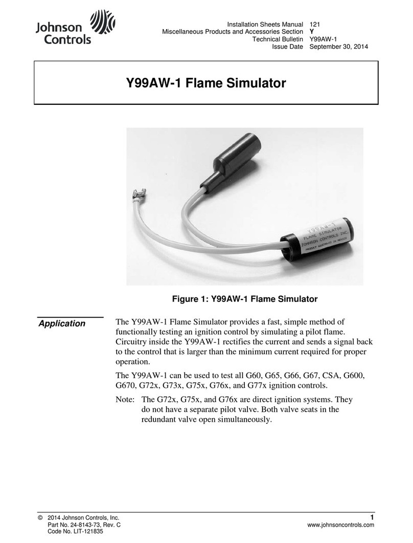
Johnson Controls
Johnson Controls Y99AW-1 Installation Sheets Manual


