manuals.online logo
Brands
  1. Home
  2. •
  3. Brands
  4. •
  5. Texas Instruments
  6. •
  7. Motherboard
  8. •
  9. Texas Instruments ADS1271EVM User manual

Texas Instruments ADS1271EVM User manual

User's GuideSBAU107 – November 2004
ADS1271EVM & ADS1271EVM-PDK
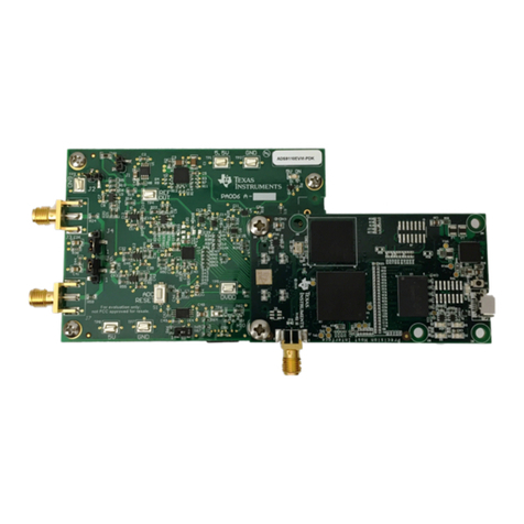
This user's guide describes the characteristics, operation, and use of theADS1271EVM, both by itself and as part of the ADS1271EVM-PDK. This EVM is a24-bit analog-to-digital converter evaluation module. A complete circuit description,schematic diagram, and bill of materials are also included.
The following related documents are available through the Texas Instruments web siteat www.ti.com .
EVM-Compatible Device Data Sheets
LiteratureDevice Number
ADS1271 SBAS306OPA350 SBOS099BOPA1632 SBOS286REF1004 SBVS002REF3125 SBVS046ASN74AVC1T45 SCES530CSN74AVC2T45 SCES531DSN74LVC1G125 SCES223LSN74LVC2G66 SCES325GSN74LVC2G157 SCES207ITPS71550 SLVS338H
Contents1 EVM Overview ............................................................................................................... 22 Analog Interface .............................................................................................................. 23 Digital Interface .............................................................................................................. 34 Power Supplies .............................................................................................................. 45 EVM Operation ............................................................................................................... 66 Kit Operation ................................................................................................................. 87 EVM Bill of Materials and Schematic .................................................................................... 12
List of Figures
1 ADS1271EVM Switch and Jumper Locations ............................................................................ 62 ADS1271EVM-PDK Block Diagram ...................................................................................... 93 Default Software Screen .................................................................................................. 10
List of Tables
1 Analog Interface Pinout (J1) ................................................................................................ 32 Auxiliary Analog Input 1 Pinout (J4) ....................................................................................... 33 Auxiliary Analog Input 2 Pinout (J5) ....................................................................................... 3
ADS1271EVM & ADS1271EVM-PDKSBAU107 – November 2004 1
www.ti.com
1 EVM Overview
1.1 Features
1.2 Introduction
2 Analog Interface
EVM Overview
4 Digital Interface Pinout (J2) ................................................................................................. 45 Power Supply Pinout ........................................................................................................ 46 Reference Selection Options - S3 and S5 ................................................................................ 57 Buffer Amplfier Options - S1 and S2 ...................................................................................... 68 ADC Analog Input Options - S4 and S6 .................................................................................. 69 ADS1271EVM Bill of Materials ........................................................................................... 12
•Full-featured evaluation board for the ADS1271 24-bit Analog-to-Digital Converter•Two ADS1271 converters on board illustrate use of daisy-chain mode•On-board reference and oscillator circuits•Modular design for use with a variety of DSP and microcontroller interface boards.•ADS1271EVM-PDK is a complete evaluation kit, which includes a USB-based motherboard andevaluation software for use with a personal computer running Microsoft Windows™ operating systems.
The ADS1271EVM is built in Texas Instruments' modular EVM form factor, which allows direct evaluationof the ADS1271 performance and operating characteristics, and eases software development and systemprototyping. This EVM is compatible with the 5-6K Interface Board (SLAU104) from Texas Instrumentsand additional third-party boards such as the HPA449 demonstration board from SoftBaugh, Inc.(www.softbaugh.com ) and the Speedy33™ from Hyperception, Inc. (www.hyperception.com ).
The ADS1271EVM-PDK is a complete evaluation/demonstration kit, which includes a USB-enabledDSP-based motherboard (the MMB0) and evaluation software for use with a PC.
The ADS1271EVM features several analog input options. Signals can be routed directly to the convertersor can pass through the on-board buffer amplifiers (U5, U6). Signals can be applied to the board throughthe standard modular EVM analog connector (J1) or brought in through the auxiliary input connectors (J4,J5). A set of switches selects which analog connector source is used and whether the buffer amplifiers arein the signal path. These switches enable several configurations for evaluation. Switch operation andanalog path configuration are described in Section 5.1 .
For maximum flexibility, the ADS1271EVM is designed for easy interfacing to multiple analog sources.Samtec part numbers SSW-110-22-F-D-VS-K and TSM-110-01-T-DV-P provide a convenient 10-pin,dual-row, header/socket combination at J1. This header/socket provides access to the analog input pins ofthe ADS1271. Consult Samtec at www.samtec.com or call 1-800-SAMTEC-9 for a variety of matingconnector options. Table 1 through Table 3 summarize the standard and auxiliary analog pinoutconfigurations.
Speedy33 is a trademark of Hyperception, Inc..Windows is a trademark of Microsoft Corp..WinZip is a trademark of WinZip Computing, Inc..
2ADS1271EVM & ADS1271EVM-PDK SBAU107 – November 2004
www.ti.com
3 Digital Interface
Digital Interface
Table 1. Analog Interface Pinout (J1)
Pin Number Signal Description
J1.1 AIN0N ADS1271 (U7) AINNJ1.2 AIN0P ADS1271 (U7) AINPJ1.3 AIN1N ADS1271 (U8) AINNJ1.4 AIN1P ADS1271 (U8) AINPJ1.5 UnusedJ1.6 UnusedJ1.7 UnusedJ1.8 UnusedJ1.15 UnusedJ1.18 REF(-) External reference source low sideJ1.20 REF(+) External reference source input (2.5V NOM)J1.9-J1.19 (odd) GND Analog ground connections (except J1.15)J1.10-J1.16 (even) Unused
Table 2. Auxiliary Analog Input 1 Pinout (J4)
Pin Number Signal Description
J4.1 AUX1P Auxiliary Signal Input 1 - Positive terminalJ4.2 AUX1N Auxiliary Signal Input 1 - Negative terminalJ4.3 AUXREF1P Auxiliary Reference Input 1 - Positive terminalJ4.4 AUXREF1N Auxiliary Reference Input 1 - Negative terminalJ4.5 GND Ground
Table 3. Auxiliary Analog Input 2 Pinout (J5)
Pin Number Signal Description
J5.1 AUX2P Auxiliary Signal Input 2 - Positive terminalJ5.2 AUX2N Auxiliary Signal Input 2 - Negative terminalJ5.3 AUXREF2P Auxiliary Reference Input 2 - Positive terminalJ5.4 AUXREF2N Auxiliary Reference Input 2 - Negative terminalJ5.5 GND Ground
The ADS1271EVM is designed to easily interface with multiple control platforms. Samtec part numbersSSW-110-22-F-D-VS-K and TSM-110-01-T-DV-P provide a convenient 10-pin, dual-row, header/socketcombination at J2. This header/socket provides access to the digital control and serial data pins of theADS1271. Consult Samtec at www.samtec.com or call 1-800-SAMTEC-9 for a variety of mating connectoroptions.
Because the ADS1271 devices are capable of daisy-chaining, this EVM has been designed to permitstacking; up to 4 EVMs can be stacked, allowing for 8 devices to be placed in a signal chain. Toaccomodate stacking of EVMs, J2 has some different connections on the top and the bottom side of theboard. Differences between top and bottom connectors are highlighted in Table 4 .
SBAU107 – November 2004 3ADS1271EVM & ADS1271EVM-PDK
www.ti.com
4 Power Supplies
Power Supplies
Table 4. Digital Interface Pinout (J2)
Pin Number Signal Description
J2.1 SYNC Synchronization ControlJ2.2 MODE0 0 = High-Speed Mode1 = Low-Power Mode(In either case, only if Mode1=1)J2.3 CLKX CLKXMODE = 1: master clock outputCLKXMODE = 0: no connectionJ2.4 DGND Digital groundJ2.5 SCLK Serial ClockJ2.6 MODE1 0 = High-Resolution Mode1 = Mode determined by MODE0J2.7 Unused.J2.8 FSDIR Indicates FSR direction:0 = Output (DRDY in SPI mode)1 = Input (FSYNC mode)J2.9 Top: FSOUT FSOUT: in FSYNC mode, copy of FSR; in SPI mode, not connectedBottom: FSR FSR: in FSYNC mode, frame-sync input; in SPI mode, DRDY output from U8J2.10 DGND Digital groundJ2.11 UnusedJ2.12 CLKRMODE 0 = Use CLKR for SPI Clock1 = Use ADC Clock for SPI clockJ2.13 Top: DIN Top: Serial data inputBottom: DOUT Bottom: Serial data outputJ2.14 CLKXMODE 0 = CLKX is High Z1 = CLKX outputs ADC master clockJ2.15 UnusedJ2.16 SCL I
2
C bus serial clockJ2.17 EXTCLK External ADC clock inputJ2.18 DGND Digital groundJ2.19 OBCLKSEL Onboard Clock Select:High to select onboard clock instead of external clock.J2.20 SDA I
2
C bus data line
J3 provides connection to the common power bus for the ADS1271EVM. Power is supplied on the pinslisted in Table 5 .
Table 5. Power Supply Pinout
Signal Pin Number Signal
+AVDD: +15V to power buffer amplifier section 1 2 –AVDD: –15V to power buffer amplifier section+5VA 3 4 UnusedDGND 5 6 AGND+1.8VD 7 8 Unused+3.3VD 9 10 +5VD
ADS1271EVM & ADS1271EVM-PDK4 SBAU107 – November 2004
www.ti.com
4.1 ADC Power
4.2 Stand-Alone Operation
4.3 Reference Voltage
Power SuppliesWhen power is supplied to J3, J6 allows for either 3.3V or 1.8V to be applied to the digital sections of theADS1271. J6 also provides for a method of measuring AVDD and DVDD supply currents if the shunts onJ6.1-2, J6.3-4, J6.5-6, and J6.7-8 are removed and a current meter is connected between the appropriatepins. See the schematic and printed circuit board silkscreen for details.
Power for the ADS1271 analog supply voltage (AVDD) comes from +5V
A
, which is supplied through J3.3.The shunt from J6 pins 1 to 2 applies this supply to the U7 ADS1271 device, while the shunt from J6 pins5 to 6 applies this supply to the U8 ADS1271.
The ADS1271 digital supply voltage (DVDD) is selected using J6. When a shunt is applied from J6 pins 9to 10, +1.8VD is selected, and this power comes from J3.7. If a shunt is placed from J6 pins 11 to 12 (thedefault factory setting), +3.3V
D
is selected, which is provided from J3.9. J6 pins 13 and 15 provide ameans of connecting analog and digital grounds to the EVM; these grounds come from J3.6 and J3.5,respectively. These grounds are always connected together at the EVM.
CAUTIONVerify that all power supplies are within the safe operating limits shown onthe ADS1271 data sheet before applying power to the EVM. Note that ashunt should only be connected between J6 pins 9 and 10 OR pins 11 and12, but never both; doing so would short the +3.3V supply to the +1.8Vdigital supply.
When used as a stand-alone EVM, the analog power can be applied to J6.2 and J6.6, referenced toJ6.13. DVDD can be applied to J6.4 and J6.8, referenced to J6.15. Note that this EVM uses only a singleground plane.
The ADS1271 requires an external voltage reference. Two switches, S3 and S5, select the source of thereference for the two ADS1271s on the EVM. An external reference may be supplied through J1 pin 20 onthe ADS1271EVM, or through J4 and J5, the auxiliary analog input connectors. A 2.5V reference isprovided on the EVM for convenience. These different reference sources can be selected using S3 andS5, as shown in Table 6 .
CAUTIONVerify that the external reference voltage is within the safe operating limitsshown on the ADS1271 data sheet before applying power to the EVM.
Table 6. Reference Selection Options - S3 and S5
S3/S5 Position Reference Inputs
Left Onboard 2.5V referenceMiddle External Reference from J1.20 (REFP) referenced to J1.18(REFN)Right S3: AUXREF1 from J4.3 referenced to J4.4S5: AUXREF2 from J5.3 referenced to J5.4
ADS1271EVM & ADS1271EVM-PDKSBAU107 – November 2004 5
www.ti.com
5 EVM Operation
LEFT MIDDLE
RIGHT
5.1 Analog Input
EVM Operation
The following section provides information on the analog input, digital control, and general operatingconditions of the ADS1271EVM. Refer to Figure 1 for switch and jumper locations, and the meanings ofleft,middle and right for switch settings in the following discussion.
Figure 1. ADS1271EVM Switch and Jumper Locations
The analog input sources can be applied directly to J1 (top or bottom side) or through the auxiliaryconnectors J4 and J5. The analog input signals can be routed directly to the two ADS1271s on the EVM,or they can be routed through an optional buffer amplifier stage built around U5 or U6. Consult theADS1271 data sheet to determine the maximum analog input range. Table 7 summarizes the position ofswitches S1 and S2. S4 and S6 can be used to select the routing of the ADS1271 analog inputs as shownin Table 8 .
Table 7. Buffer Amplfier Options - S1 and S2
S1/S2 Position Analog Inputs
Top Input from J1Middle Input from J4/J5 auxiliary inputsBottom No connection
Table 8. ADC Analog Input Options - S4 and S6
S4/S6 Position Analog Inputs
Left Input from Buffer AmplifierMiddle Input from J1Right Input from J4/J5 auxiliary inputs
ADS1271EVM & ADS1271EVM-PDK SBAU107 – November 20046
www.ti.com
5.2 Digital Control
5.3 Communication Modes
EVM Operation
5.1.1 Buffer Amplifiers
The buffer amplifiers on this EVM are OPA1632s (U5, U6). These amplifiers are optimized for ACperformance and are configured as fully-differential unity gain buffers. They require ±15V supplies, whichare provided from J3 pins 1 and 2.
The OPA1632 requires a common mode voltage, which is provided on this EVM by U2 and U3. Someusers may not wish to use the buffer amplifier section and provide the ±15V supplies. If the ±15V suppliesare not connected, then having a voltage on the V
OCM
pins of the amplifiers would exceed their maximumratings. Thus, U2 and U3 provide a separate 2.5V reference for the buffer amplifier section rather thanusing the same reference as the ADS1271, which would always be powered. For this reason, U2 and U3power is provided through a separate regulator, U11.
The digital control signals can be applied directly to J2. The modular ADS1271EVM can also beconnected directly to a DSP or microcontroller interface board, such as the HPA449. For a current list ofcompatible interface and/or accessory boards for the EVM or the ADS1271, see the relevant productfolder on the TI web site.
The ADS1271EVM has a digital routing network which can help simulate several possible systemconnections. The routing network also provides level-shifting, which allows the ADS1271 to be operated atany supported logic level regardless of the logic level used on J2. Note that you are not required to includethis circuitry in your own designs; typically no glue logic is required to connect one or more ADS1271s to aprocessor.
5.3.1 Routing control
Routing is controlled by pins CLKRMODE, CLKXMODE, and OBCLKSEL on J2. CLKRMODE controls thedirection and connection of CLKR. When CLKRMODE is low, CLKR is an input connected only to SCLK.When CLKRMODE is high, CLKR becomes an output connected to SCLK, and SCLK is tied to CLK. Thisconnection can be useful in both FSYNC and SPI modes. A pulldown on CLKRMODE makes FSYNCmode the default setting.
When CLKXMODE is high, CLKX is an output connected to CLK. This setting is primarily useful for certainconfigurations using TI's McBSP, where CLKX can be used as a reference clock input for the serial port.When CLKXMODE is low, CLKX on J2 is unconnected. A pulldown on CLKXMODE makes thisconfiguration the default.
OBCLKSEL selects between one of two master clock sources. When OBCLKSEL is high, the on-boardclock is active and used for the master clock. When OBCLKSEL is low, the master clock is taken fromEXTCLK on J2, and the on-board oscillator is disabled. A pulldown on OBCLKSEL makes this setting thedefault.
5.3.2 Using the ADS1271 communication modes
You can use either of the two ADS1271 interface modes with the ADS1271EVM. The interface modes arechosen manually using switch S7, and cannot be selected electrically.
The FSR and FSOUT pins on J2 operate differently depending on the communication mode. In SPI mode,FSR, which is on the socket on the bottom side of the board, carries the DRDY output signal from the firstADC (U8), the second ADC (U7) DRDY line is not connected, and the FSOUT pin on the header on thetop side of the board is not connected. In FSYNC mode, the FSYNC pins of both ADCs are tied together,and the signal on FSR is copied to the top connector on pin FSOUT.
ADS1271EVM & ADS1271EVM-PDKSBAU107 – November 2004 7
www.ti.com
5.4 Clock Source
6 Kit Operation
Kit Operation
This arrangement allows the ADS1271EVM to be stacked with other ADS1271EVMs in either mode, aslong as all boards in the stack are in the same mode.
A motherboard can sense which state the switch is in and configure itself appropriately by monitoring theFSDIR pin on J2. This pin is high when FSOUT is active and FSR is an input, and low when FSOUT isdisconnected and FSR is an output (that is, it carries the DRDY signal).
5.4.1 Onboard Oscillator
The ADS1271 requires a clock. A 25MHz clock oscillator is provided on the EVM, and is selected as theclock source for the device when OBCLKSEL (J2.19) is high.
5.4.2 External Oscillator
When OBCLKSEL (J2.19) is low, the clock source for the ADS1271 is provided from J2.17, and theon-board clock oscillator is shut down.
The following section provides informationon using the ADS1271EVM-PDK, including setup, programinstallation, and program usage.
ADS1271EVM & ADS1271EVM-PDK8 SBAU107 – November 2004
www.ti.com
6.1 ADS1271EVM-PDK Block Diagram
C5507
DSP USB
EVM Connectors
ADS1271EVM
Control and Data
Interface
MMB0
6.2 Quick Start
Kit Operation
A block diagram of the ADS1271EVM-PDK is shown in Figure 2 . The evaluation kit consists of two printedcircuit boards connected together. The motherboard is designated as the MMB0, while the daughtercard isthe ADS1271EVM described previously in this manual.
Figure 2. ADS1271EVM-PDK Block Diagram
Ensure that the ADS1271EVM is installed on the MMB0. Place the CD-ROM into your PC CD-ROM drive.Locate the Setup program on the disk and execute it. The Setup program installs the ADS1271 evaluationsoftware on your PC. Follow the instructions and prompts given.
After the main program is installed, a dialog box appears with instructions for installing NI-VISA 3.1Runtime, a self-extracting archive. Click OK to proceed. A WinZip™ dialog appears. Click Unzip, and thearchive extracts itself and automatically runs the NI-VISA 3.1 Runtime installer.
Follow the instructions in the NI-VISA 3.1 Runtime Installer. When prompted for which features to install,do the following:
1. Click on the disk icon next to NI-VISA 3.12. Select, Do not install this feature.3. Click on the disk icon next to USB.4. Select the option which installs this feature.5. Click Next.
Accept the license agreement, and continue the installation.
ADS1271EVM & ADS1271EVM-PDKSBAU107 – November 2004 9
www.ti.com
6.3 Program Description
Kit Operation
When the installation completes, click Finish on the ADS1271EVM installer window. You may be promptedto restart your computer.
When installation is complete, attach a USB cable from your PC to the MMB0. Supply power to J14 on theMMB0, following the silkscreen markings or schematic; this will supply the ADS1271EVM power throughthe J3 connector on the ADS1271EVM.
The software should automatically find the ADS1271EVM, and a screen similar to the one in Figure 3should appear.
Figure 3. Default Software Screen
Once the ADS1271EVM-PDK software (described in Section 6.2 ) is installed, evaluation and developmentwith the ADS1271 can begin.
6.3.1 Basic Usage
When the program runs, it checks to see whether an MMB0 is connected. If it is, the program downloadsthe firmware to it, and runs; otherwise, it shows a dialog box telling you that it cannot find an MMB0. If yousee this, make sure the MMB0 is connected and powered on, correct this if necessary, and click Retry. Ifyou cannot fix the problem, click Cancel to quit.
ADS1271EVM & ADS1271EVM-PDK10 SBAU107 – November 2004
www.ti.com
Kit Operation
After the program loads the MMB0 successfully, you will see a screen similar to that shown in Figure 3 .The top display shows an FFT of the ADC output up to the Nyquist frequency (half the sampling rate), andcertain AC analysis numbers. Below this are a number of controls and meters, and at the bottom is a setof tabs, which show either a histogram, a picture of the incoming waveform, or the data recording controls.
To exit the program, select File -> Exit from the menu bar.
When the program starts, it is idle. You can put it in either Acquire mode or Record mode.
6.3.1.1 Acquire Mode
To put the program into Acquire mode, click the Acquire button. In Acquire mode, the ADS1271EVMsoftware collects data as quickly as possible from the board in 2,048-sample blocks and analyzes it. BothAC and DC analyses are performed.
In Acquire mode, you can only view the data from one channel at a time. To choose channels, use theChannel box.
AC analysis consists of the FFT display and THD analysis. For THD analysis to work, the input must be asine wave below half the Nyquist frequency, since the THD analyzer needs at least one harmonic to workfrom. The THD analyzer uses an automatic tone-detection algorithm, which searches for the highestharmonic and uses that for THD analysis. The frequency it detects is shown in the indicator marked ToneFreq. This frequency may not be exactly what your oscillator is set for, but it should generally be veryclose.
For DC analysis, the program provides DC RMS noise (standard deviation), peak amplitude, and a DClevel meter. A histogram is also provided; this is visible in the left tab. Basic DC measurements work bestwhen the ADC is driven by an amplifier or stable voltage source; shorting the inputs also works.
6.3.1.2 Record Mode
To record data, go to the Record To File tab and do the following:1. If Acquire is on, turn it off. You cannot start recording when Acquire is on.2. Set the Conversion Mode and Sample Rate fields to the settings you want to record with. The channelselector has no effect for data recording.3. Enter a path in the Destination File field. You can use the folder icon to browse for the file with astandard file dialog. If the file you enter cannot be opened or created, the record button will bedisabled. If the path points to an existing file, the file will be overwritten when you activate recording.4. Enter a number of samples to convert. You can enter this in time or number of samples; the other boxwill update automatically. The number of samples is limited by available memory on the MMB0.5. Click the record button. You will see the Samples Retrieved bar graph increase. When it reaches thenumber of samples you selected, recording will stop and the record button will go dark.
After this, the file you selected will contain comma-separated decimal numbers collected from the ADCs.The samples are written two to a line, with the sample from Channel 1 first, followed by a comma, followedby the sample from Channel 2. This kind of file can easily be imported into a spreadsheet, among otherapplications.
6.3.1.3 Configuration
You can set the sample rate and conversion mode. Sample rate and conversion mode are always thesame for each ADS1271 being evaluated; you cannot set one channel to a different parameter.
The ADS1271's three conversion modes are selected from the flip-menu labelled Conversion Mode.
The ADS1271 clock is normally generated by a PLL synthesizer on the MMB0. The synthesizer cannotsynthesize all frequencies precisely; the software will come as close as it can, but in some cases thesample rate will be slightly off.
ADS1271EVM & ADS1271EVM-PDKSBAU107 – November 2004 11
www.ti.com
7 EVM Bill of Materials and Schematic
EVM Bill of Materials and SchematicWhen you change the sample rate, you may find the value clamped or altered. The limits are different forhigh-speed mode: in that mode, the maximum sampling rate is approximately 105ksps, but in the othermodes, it is approximately 52.5ksps. If you have the sampling rate set too high when you switch toanother mode, the program will automatically reduce the rate to the maximum rate allowed for that mode.
Note that the block size does not change. When you reduce the sampling rate, waveforms will appear togo up in frequency.
The following table contains a complete bill of materials for the modular ADS1271EVM.
Table 9. ADS1271EVM Bill of Materials
Designators Description Manufacturer Mfg. Part Number
R15, R16, R17, R18, R23, 47 Ω1/8W 5% Chip Resistor Panasonic ERJ-3GEYJ470VR24, R25, R26R7, R8, R9, R10, R11, R12, 1K Ω1/16W 1% Chip Resistor Panasonic ERJ-3EKF1001VR13, R14R2 10K Ω1/10W 5% Chip Resistor Panasonic ERJ-3GEYJ103VR1 24.9K Ω1/16W 1% Chip Resistor Panasonic ERJ-3EKF2492VR3, R4, R21, R22 47K Ω1/10W 5% Chip Resistor Panasonic ERJ-3GEYJ473VR5, R6 100K Ω1/10W 5% Chip Resistor Panasonic ERJ-3GEYJ104VR19, R20 470K Ω1/10W 5% Chip Resistor Panasonic ERJ-3GEYJ474VC20, C21, C22, C23 100pF 50V Ceramic TDK C1608C0G1H101JTChip Capacitor, ±5%, C0GC6, C7, C8, C9, C24, C25 1nF 50V Ceramic TDK C1608C0G1H102JTChip Capacitor, ±5%, C0GC28 0.01µF 50V Ceramic TDK C1608X7R1H103KTChip Capacitor, ±5%, X7RC26, C27, C30, C31 0.1µF 50V Ceramic TDK C1608X7R1H104KTChip Capacitor, ±10%, X7RC1, C3, C4, C5, C29 1µF 16V Ceramic TDK C1608X7R1C105KTChip Capacitor, ±10%, X7RC13, C14, C15, C16, C18, 10µF 6.3V Ceramic TDK C2012X5R0J106MTC19 Chip Capacitor, ±20%, X5RC10, C11, C12, C17 10µF 25V Ceramic TDK C3225X7R1E106MTChip Capacitor, ±20%, X5RC2 100µF 10V Low ESR Kemet T520D107M010ASE055Tantalum Capacitor, ±20%U1 Precision Voltage Reference Texas Instruments REF1004I-2.5U2, U3 Precision Voltage Reference Texas Instruments REF3125AIDBZU4 Precision Operational Amplifier Texas Instruments OPA350UAU5, U6 Fully Differential Amplifier Texas Instruments OPA1632DGNU7, U8 Precision Delta-Sigma ADC Texas Instruments ADS1271IPWU9, U10 Dual Analog Switch Texas Instruments SN74LVC2G66DCTU11 LDO Voltage Regulator, Texas Instruments TPS1550DCKHigh Input VoltageU12 Single, 2-Line to 1 Data Selec- Texas Instruments SN74LVC2G157DCTtor/MultiplexerU13 3.3V Oscillator CTS CB3LV-5I-27-M0000U15, U16 Dual Split Rail Level Shifter Trans- Texas Instruments SN74AVC2T45DCTceiverU17, U18 Split Rail Level Shifter Transceiver Texas Instruments SN74AVC1T45DBV
ADS1271EVM & ADS1271EVM-PDK12 SBAU107 – November 2004
www.ti.com
7.1 ADS1271EVM Schematic
EVM Bill of Materials and Schematic
Table 9. ADS1271EVM Bill of Materials (continued)
Designators Description Manufacturer Mfg. Part Number
U19 Dual Split Rail Level Shifter Trans- Texas Instruments SN74AVCH2T45DCTceiverU20 Tri-State Buffer Texas Instruments SN74LVC1G125DBVADS1271EVM PCB Texas Instruments 6466987J1A, J2T 20-pin SMT Plug Samtec TSM-110-01-L-DV-PJ1B, J2B 20-pin SMT Socket Samtec SSW-110-22-F-D-VS-KJ3A 10-pin SMT Plug Samtec TSM-105-01-L-DV-PJ3B 10-pin SMT Socket Samtec SSW-105-22-F-D-VS-KJ4, J5 Terminal Strip, 5 pin (5x1), Right Samtec TSW-105-08-L-S-RAAngleJ6 Terminal Strip, 16-pin (8x2) Samtec TSW-108-07-L-DJ7 Terminal Strip, 4-pin (2x2) Samtec TSW-102-07-L-DS1, S2, S3, S4, S5, S6 Dual Pole 3 Position Switch E-Switch EG2305AS7 SPDT Switch Tyco-Alcoswitch SLS121PCTP1 Miniature Test Point Terminal Keystone Electronics 5000Header Shorting Block Samtec SNT-100-BK-T
The schematic diagram is provided as a reference.
ADS1271EVM & ADS1271EVM-PDKSBAU107 – November 2004 13
1 2 3 4 5 6
A
B
C
D
6
54321
D
C
B
A
ti
6730 SOUTH TUCSON BLVD., TUCSON, AZ 85706 USA
TITLE
SHEET OF FILE
SIZE DATE REV21 OCT 2004
DRAWN BY
EN INEER
REVISION HISTORY
REV EN INEERIN CHAN E NUMBER APPROVED
B
DATA ACQUISITION PRODUCTS
HI H-PERFORMANCE ANALO DIVISION
SEMICONDUCTOR ROUP
M. P. ASHTON
M. P. ASHTON
C
1 1
ADS1271EVM
DOCUMENT CONTROL NO. 6466898
AN0+ 2
AN1+ 4
AN2+ 6
AN3+ 8
AN4+ 10
AN5+ 12
AN6+ 14
AN7+ 16
REF- 18
REF+ 20
A ND
17
A ND
19
AN0-
1
AN1-
3
AN2-
5
AN3-
7
A ND
9
A ND
11
A ND
13
VCOM
15
J1
ANALO HDR
CNTL
1
CLKX
3
CLKR
5
FSX
7
FSR
9
DX
11
DR
13
INT
15
TOUT
17
PIO5
19
PIO0 2
D ND 4
PIO1 6
PIO2 8
D ND 10
PIO3 12
PIO4 14
SCL 16
D ND 18
SDA 20
J2T
SERIALHDR
C2
100U
AINP
1
AINN
2
A ND
3
AVDD
4
MODE 5
FORMAT 6
SYNC/PDWN 7
DIN 8
DOUT 9
DRDY/FSYNC 10
SCLK 11
CLK 12
DVDD 13
D ND 14
VREFN
15
VREFP
16
U7
ADS1271PW
AINP
1
AINN
2
A ND
3
AVDD
4
MODE 5
FORMAT 6
SYNC/PDWN 7
DIN 8
DOUT 9
DRDY/FSYNC 10
SCLK 11
CLK 12
DVDD 13
D ND 14
VREFN
15
VREFP
16
U8
ADS1271PW
CNTL
1
CLKX
3
CLKR
5
FSX
7
FSR
9
DX
11
DR
13
INT
15
TOUT
17
PIO5
19
PIO0 2
D ND 4
PIO1 6
PIO2 8
D ND 10
PIO3 12
PIO4 14
SCL 16
D ND 18
SDA 20
J2B
SERIALHDR
OBCLKSEL
+3.3VD
DVDD
MODE1
EXTCLK
TP1
CLK
S4
SW-DP3T
S6
SW-DP3T
C24 1N
C21
100P
C20
100P
C26
100N
C27
100N
+
8
2
-
1
3
6
4
5
+
-
VOCM
U5
OPA1632
IN
1OUT 2
ND
3
U3
REF3125AIDBZ
R15
47
R16 47
R10 1K
C10
10U
C6
1N C0
C7
1N C0
C11
10U
+AVDD
-AVDD
R11
1K
R7
1K
R8
1K
R5
100K
+
8
2
-
1
3
6
4
5
+
-
VOCM
U6
OPA1632
R17 47
R18 47
R12
1K
C12
10U
C8
1N C0
C9
1N C0
C17
10U
+AVDD
-AVDD
R14
1K
R9
1K
R13
1K
R6
100K
1
2
3
4
5
J5
HEADER-5
1
2
3
4
5
J4
HEADER-5
C18
10U
C13
10U
IN
4
ND
2OUT 5
U11
TPS71550DCK
C5
1U
C4
1U
+AVDD
S1
SW-DP3T
S2
SW-DP3T
AUXREF1P
AUXREF1N
AUX1P
AUX1N
AUX2P
AUX2N
AUXREF2P
AUXREF2N
S3
SW-DP3T
S5
SW-DP3T
C25 1N
C23
100P
C22
100P
REFP
REFN
AUXREF1P
AUXREF1N
REFP
AUXREF2P
REFN
AUXREF2N
AMPOUT2P
AMPOUT2N
AIN1P
AIN1N
AIN0P
AIN0N
AUX1P
AUX1N
AUX2P
AUX2N
C14
10U
ADCAVDD2
C19
10U
C16
10U
ADCDVDD2
ADCDVDD1
C15
10U
ADCAVDD1
AIN0N
AIN0P
AIN1P
AIN1N
AIN1N AIN1P
AIN0PAIN0N
REFN
REFP
+AVDD
-AVDD
+5V
DVDD
1 2
3 4
5 6
7 8
9 10
11 12
13 14
15 16
J6
JPR-2X8
DVDD +5V
ADCDVDD1
ADCDVDD2
ADCAVDD1
ADCAVDD2
D1V8IN
A NDIN
D NDIN
IN
1OUT 2
ND
3
U2
REF3125AIDBZ
4
8
6
U1
REF1004I-2.5
R2
10K
R1
24.9K 1%
+5V
C1
1U 16V X7R
+5V
OBREF
C3
1U
OBCLK
+3.3VD
EOH
1
ND 2
OUT
3VCC 4
U13
CTS_CB3LV-3C-25.0000-T
+3.3VD
C28
10N
DVDD
C29
1U
1A
11B 2
2C
3
ND 4
2A
52B 6
1C
7VCC 8
U10
SN74LVC2 66DCT
A1
B2
Y
3
ND 4
Y
5A/B 6
7
VCC
8
U12
SN74LVC2 157DCT
1A
11B 2
2C
3
ND 4
2A
52B 6
1C
7VCC 8
U9
SN74LVC2 66DCT
S7
ALC_SLS121PC
CLKRMODE
FORMAT
R20
470K
R21
47K
R22
47K
J1A (TOP) = SAM_TSM-110-01-L-DV-P
J1B (BOTTOM) = SAM_SSW-110-22-F-D-VS-K
J3A (TOP) = SAM_TSM-105-01-L-DV-P
J3B (BOTTOM) = SAM_SSW-105-22-F-D-VS-K
2
3
6
74
U4
OPA350UA VCCA 1
A1 2
A2 3
ND 4
VCCB
8
B1
7
B2
6
DIR
5
U15
SN74AVC2T45DCT
VCCA 1
A1 2
A2 3
ND 4
VCCB
8
B1
7
B2
6
DIR
5
U16
SN74AVC2T45DCT
+3.3VDDVDD
2 4
1
53
U20
SN74LVC1 125DBV
MODE
FSDIR
FMTSEL
FORMAT
MODE0
DVDD
CLKX
FSR
FSOUT
FSOUT
DOUT
FSR
CLKX
VCCA 1
ND 2
A3
B
4
DIR
5
VCCB
6
U17
SN74AVC1T45DBV
VCCA
1
ND
2A
3B4
DIR 5
VCCB 6
U18
SN74AVC1T45DBV
DOUT
DIN
CLKR
VCCA
1
A1
2
A2
3
ND
4
VCCB 8
B1 7
B2 6
DIR 5
U19
SN74AVCH2T45DCT
SYNC
DVDD +3.3VD
FSDIR
FSDIR
DOUT_1
FSR_1
FSOUT_1
1 2
3 4
J7
JPR-2X2
MODE0 MODE
R3
47K
DVDD
CLKXMODE
SCLK
DVDD
CLKRMODE
CLKX_1
CLKXMODE
CLK
FSYNC2
FSYNC1 FSYNC2
SCLK
DIN2
DIN1
DOUT1
SYNC_1
FSDIR
CLK
DIN2
FSYNC1
DOUT1
FSYNC1
DVDD = FSYNC
ND = SPI
R19
470K
R4
47K
CLK
FMTSEL
CLKRMODE
DVDD
DVDD
DVDD
+3.3VD
+3.3VD
+3.3VD
FSOUT_1
SYNC
DIN
FSDIR
MODE0
MODE1
R24
47 R25
47
R23
47
R26
47
+VA
1-VA 2
+5VA
3-5VA 4
D ND
5A ND 6
+1.8VD
7VD1 8
+3.3VD
9+5VD 10
J3
POWERHDR
C30 100N
C31 100N
FCC Warnings
This equipment is intended for use in a laboratory test environment only. It generates, uses, and can radiate radio frequencyenergy and has not been tested for compliance with the limits of computing devices pursuant to subpart J of part 15 of FCC rules,which are designed to provide reasonable protection against radio frequency interference. Operation of this equipment in otherenvironments may cause interference with radio communications, in which case the user at his own expense will be required totake whatever measures may be required to correct this interference.
EVM IMPORTANT NOTICE
Texas Instruments (TI) provides the enclosed product(s) under the following conditions:This evaluation kit being sold by TI is intended for use for ENGINEERING DEVELOPMENT OR EVALUATION PURPOSES ONLYand is not considered by TI to be fit for commercial use. As such, the goods being provided may not be complete in terms ofrequired design-, marketing-, and/or manufacturing-related protective considerations, including product safety measures typicallyfound in the end product incorporating the goods. As a prototype, this product does not fall within the scope of the European Uniondirective on electromagnetic compatibility and therefore may not meet the technical requirements of the directive.Should this evaluation kit not meet the specifications indicated in the EVM User's Guide, the kit may be returned within 30 daysfrom the date of delivery for a full refund. THE FOREGOING WARRANTY IS THE EXCLUSIVE WARRANTY MADE BY SELLERTO BUYER AND IS IN LIEU OF ALL OTHER WARRANTIES, EXPRESSED, IMPLIED, OR STATUTORY, INCLUDING ANYWARRANTY OF MERCHANTABILITY OR FITNESS FOR ANY PARTICULAR PURPOSE.The user assumes all responsibility and liability for proper and safe handling of the goods. Further, the user indemnifies TI from allclaims arising from the handling or use of the goods. Please be aware that the products received may not be regulatory compliantor agency certified (FCC, UL, CE, etc.). Due to the open construction of the product, it is the user's responsibility to take any and allappropriate precautions with regard to electrostatic discharge.EXCEPT TO THE EXTENT OF THE INDEMNITY SET FORTH ABOVE, NEITHER PARTY SHALL BE Liable to the other FORANY INDIRECT, SPECIAL, INCIDENTAL, OR CONSEQUENTIAL DAMAGES.TI currently deals with a variety of customers for products, and therefore our arrangement with the user is not exclusive.TI assumes no liability for applications assistance, customer product design, software performance, or infringement ofpatents or services described herein.
Please read the EVM User's Guide and, specifically, the EVM Warnings and Restrictions notice in the EVM User's Guide prior tohandling the product. This notice contains important safety information about temperatures and voltages. For further safetyconcerns, please contact the TI application engineer.Persons handling the product must have electronics training and observe good laboratory practice standards.No license is granted under any patent right or other intellectual property right of TI covering or relating to any machine, process, orcombination in which such TI products or services might be or are used.
EVM WARNINGS AND RESTRICTIONS
It is important to operate this EVM within the input voltage range of 1.8 V to 5 V and the output voltage range of 0 V to 5 V.Exceeding the specified input range may cause unexpected operation and/or irreversible damage to the EVM. If there arequestions concerning the input range, please contact a TI field representative prior to connecting the input power.Applying loads outside of the specified output range may result in unintended operation and/or possible permanent damage to theEVM. Please consult the EVM User's Guide prior to connecting any load to the EVM output. If there is uncertainty as to the loadspecification, please contact a TI field representative.During normal operation, some circuit components may have case temperatures greater than 30 °C. The EVM is designed tooperate properly with certain components above 85 °C as long as the input and output ranges are maintained. These componentsinclude but are not limited to linear regulators, switching transistors, pass transistors, and current sense resistors. These types ofdevices can be identified using the EVM schematic located in the EVM User's Guide. When placing measurement probes nearthese devices during operation, please be aware that these devices may be very warm to the touch.
Mailing Address: Texas Instruments, Post Office Box 655303, Dallas, Texas 75265Copyright © 2004, Texas Instruments Incorporated
IMPORTANT NOTICE
Texas Instruments Incorporated and its subsidiaries (TI) reserve the right to make corrections, modifications,
enhancements, improvements, and other changes to its products and services at any time and to discontinue
any product or service without notice. Customers should obtain the latest relevant information before placing
orders and should verify that such information is current and complete. All products are sold subject to TI’s terms
and conditions of sale supplied at the time of order acknowledgment.
TI warrants performance of its hardware products to the specifications applicable at the time of sale in
accordance with TI’s standard warranty. Testing and other quality control techniques are used to the extent TI
deems necessary to support this warranty. Except where mandated by government requirements, testing of all
parameters of each product is not necessarily performed.
TI assumes no liability for applications assistance or customer product design. Customers are responsible for
their products and applications using TI components. To minimize the risks associated with customer products
and applications, customers should provide adequate design and operating safeguards.
TI does not warrant or represent that any license, either express or implied, is granted under any TI patent right,
copyright, mask work right, or other TI intellectual property right relating to any combination, machine, or process
in which TI products or services are used. Information published by TI regarding third-party products or services
does not constitute a license from TI to use such products or services or a warranty or endorsement thereof.
Use of such information may require a license from a third party under the patents or other intellectual property
of the third party, or a license from TI under the patents or other intellectual property of TI.
Reproduction of information in TI data books or data sheets is permissible only if reproduction is without
alteration and is accompanied by all associated warranties, conditions, limitations, and notices. Reproduction
of this information with alteration is an unfair and deceptive business practice. TI is not responsible or liable for
such altered documentation.
Resale of TI products or services with statements different from or beyond the parameters stated by TI for that
product or service voids all express and any implied warranties for the associated TI product or service and
is an unfair and deceptive business practice. TI is not responsible or liable for any such statements.
Following are URLs where you can obtain information on other Texas Instruments products and application
solutions:
Products Applications
Amplifiers amplifier.ti.com Audio www.ti.com/audio
Data Converters dataconverter.ti.com Automotive www.ti.com/automotive
DSP dsp.ti.com Broadband www.ti.com/broadband
Interface interface.ti.com Digital Control www.ti.com/digitalcontrol
Logic logic.ti.com Military www.ti.com/military
Power Mgmt power.ti.com Optical Networking www.ti.com/opticalnetwork
Microcontrollers microcontroller.ti.com Security www.ti.com/security
Telephony www.ti.com/telephony
Video & Imaging www.ti.com/video
Wireless www.ti.com/wireless
Mailing Address: Texas Instruments
Post Office Box 655303 Dallas, Texas 75265
Copyright 2004, Texas Instruments Incorporated

This manual suits for next models

1

Other Texas Instruments Motherboard manuals

Texas Instruments DRV8303EVM User manual

Texas Instruments

Texas Instruments DRV8303EVM User manual

Texas Instruments TAS5753MDEVM User manual

Texas Instruments

Texas Instruments TAS5753MDEVM User manual

Texas Instruments TPS40100 User manual

Texas Instruments

Texas Instruments TPS40100 User manual

Texas Instruments BQ2515 EVM Series User manual

Texas Instruments

Texas Instruments BQ2515 EVM Series User manual

Texas Instruments AN-1574 LM5073 User manual

Texas Instruments

Texas Instruments AN-1574 LM5073 User manual

Texas Instruments BOOSTXL-DRV8323Rx User manual

Texas Instruments

Texas Instruments BOOSTXL-DRV8323Rx User manual

Texas Instruments TPS25944XEVM-635 User manual

Texas Instruments

Texas Instruments TPS25944XEVM-635 User manual

Texas Instruments ADS86 EVM-PDK Series User manual

Texas Instruments

Texas Instruments ADS86 EVM-PDK Series User manual

Texas Instruments LMK00101BEVAL/NOPB User manual

Texas Instruments

Texas Instruments LMK00101BEVAL/NOPB User manual

Texas Instruments TPS65300EVM User manual

Texas Instruments

Texas Instruments TPS65300EVM User manual

Texas Instruments TPS54973EVM-017 User manual

Texas Instruments

Texas Instruments TPS54973EVM-017 User manual

Texas Instruments LM5161PWPBKEVM User manual

Texas Instruments

Texas Instruments LM5161PWPBKEVM User manual

Texas Instruments TPS65980EVM User manual

Texas Instruments

Texas Instruments TPS65980EVM User manual

Texas Instruments TSW3003 User manual

Texas Instruments

Texas Instruments TSW3003 User manual

Texas Instruments TPSF12C1EVM-FILTER User manual

Texas Instruments

Texas Instruments TPSF12C1EVM-FILTER User manual

Texas Instruments TPS7B81EVM-025 User manual

Texas Instruments

Texas Instruments TPS7B81EVM-025 User manual

Texas Instruments TPSM8286 AA0 Series User manual

Texas Instruments

Texas Instruments TPSM8286 AA0 Series User manual

Texas Instruments AMC1100EVM User manual

Texas Instruments

Texas Instruments AMC1100EVM User manual

Texas Instruments DAC80502 User manual

Texas Instruments

Texas Instruments DAC80502 User manual

Texas Instruments CC2540 User manual

Texas Instruments

Texas Instruments CC2540 User manual

Texas Instruments ADC DJ Series User manual

Texas Instruments

Texas Instruments ADC DJ Series User manual

Texas Instruments TPS7B70EVM-008 User manual

Texas Instruments

Texas Instruments TPS7B70EVM-008 User manual

Texas Instruments TLV3601EVM User manual

Texas Instruments

Texas Instruments TLV3601EVM User manual

Texas Instruments LMG3410-HB-EVM User manual

Texas Instruments

Texas Instruments LMG3410-HB-EVM User manual

Popular Motherboard manuals by other brands

Gigabyte GA-7VR user manual

Gigabyte

Gigabyte GA-7VR user manual

Asus F1A75-V PRO quick start guide

Asus

Asus F1A75-V PRO quick start guide

JETWAY NF98 series Technical manual

JETWAY

JETWAY NF98 series Technical manual

Supermicro X6DH8-XG2 user manual

Supermicro

Supermicro X6DH8-XG2 user manual

Intel DQ965CO Product guide

Intel

Intel DQ965CO Product guide

Silicon Laboratories CP2112-EK user guide

Silicon Laboratories

Silicon Laboratories CP2112-EK user guide

EMAC PCA-6782 user manual

EMAC

EMAC PCA-6782 user manual

ASROCK B460M Steel Legend instructions

ASROCK

ASROCK B460M Steel Legend instructions

Asus PRIME X670E-P manual

Asus

Asus PRIME X670E-P manual

MSI H6M-P30 (B3) user manual

MSI

MSI H6M-P30 (B3) user manual

Gigabyte GA-SBCAP3350 Quick installation guide

Gigabyte

Gigabyte GA-SBCAP3350 Quick installation guide

bplan Pegasos II instruction manual

bplan

bplan Pegasos II instruction manual

ASROCK R-4130 Use and care guide

ASROCK

ASROCK R-4130 Use and care guide

austriamicrosystems AS5030 Operation manual

austriamicrosystems

austriamicrosystems AS5030 Operation manual

VIA Technologies VAB-600-A quick guide

VIA Technologies

VIA Technologies VAB-600-A quick guide

AMS AS621 Series user guide

AMS

AMS AS621 Series user guide

Linear Technology DC1317A-B quick start guide

Linear Technology

Linear Technology DC1317A-B quick start guide

National Semiconductor LM48555 quick start guide

National Semiconductor

National Semiconductor LM48555 quick start guide

manuals.online logo
manuals.online logoBrands
  • About & Mission
  • Contact us
  • Privacy Policy
  • Terms and Conditions

Copyright 2025 Manuals.Online. All Rights Reserved.