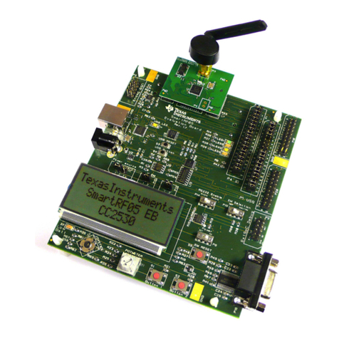
Texas Instruments TMS3637 Installation and user guide

i
TMS3637
Remote Control Transmitter/Receiver
Data Manual
SCTS037B
JUNE 1997

ii
IMPORTANT NOTICE
Texas Instruments (TI) reserves the right to make changes to its products or to
discontinue any semiconductor product or service without notice, and advises its
customers to obtain the latest version of relevant information to verify, before placing
orders, that the information being relied on is current.
TI warrants performance of its semiconductor products and related software to the
specifications applicable at the time of sale in accordance with TI’s standard warranty.
TestingandotherqualitycontroltechniquesareutilizedtotheextentTIdeemsnecessary
to support this warranty. Specific testing of all parameters of each device is not
necessarily performed, except those mandated by government requirements.
Certain applications using semiconductor products may involve potential risks of death,
personal injury, or severe property or environmental damage (“Critical Applications”).
TI SEMICONDUCTOR PRODUCTS ARE NOT DESIGNED, INTENDED,
AUTHORIZED, OR WARRANTED TO BE SUITABLE FOR USE IN LIFE-SUPPORT
APPLICATIONS, DEVICES OR SYSTEMS OR OTHER CRITICAL APPLICATIONS.
Inclusion of TI products in such applications is understood to be fully at the risk of the
customer. Use of TI products in such applications requires the written approval of an
appropriateTIofficer.Questionsconcerningpotentialriskapplicationsshouldbedirected
to TI through a local SC sales office.
In order to minimize risks associated with the customer’s applications, adequate design
and operating safeguards should be provided by the customer to minimize inherent or
procedural hazards.
TI assumes no liability for applications assistance, customer product design, software
performance, or infringement of patents or services described herein. Nor does TI
warrant or represent that any license, either express or implied, is granted under any
patent right, copyright, mask work right, or other intellectual property right of TI covering
or relating to any combination, machine, or process in which such semiconductor
products or services might be or are used.
Copyright 1997, Texas Instruments Incorporated

iii
Contents
Title Page
1 Introduction 1–1. . . . . . . . . . . . . . . . . . . . . . . . . . . . . . . . . . . . . . . . . . . . . . . . . . . . . . . . . . . . . . .
1.1 Features 1–1. . . . . . . . . . . . . . . . . . . . . . . . . . . . . . . . . . . . . . . . . . . . . . . . . . . . . . . . . . . . . .
1.2 Functional Block Diagram 1–2. . . . . . . . . . . . . . . . . . . . . . . . . . . . . . . . . . . . . . . . . . . . . . .
1.3 Terminal Assignments 1–2. . . . . . . . . . . . . . . . . . . . . . . . . . . . . . . . . . . . . . . . . . . . . . . . . .
1.4 Terminal Functions 1–3. . . . . . . . . . . . . . . . . . . . . . . . . . . . . . . . . . . . . . . . . . . . . . . . . . . . .
2 Specifications 2–1. . . . . . . . . . . . . . . . . . . . . . . . . . . . . . . . . . . . . . . . . . . . . . . . . . . . . . . . . . . . .
2.1 Absolute Maximum Ratings Over Operating Free-Air Temperature Range 2–1. . . .
2.2 Recommended Operating Conditions 2–1. . . . . . . . . . . . . . . . . . . . . . . . . . . . . . . . . . . . .
2.3 Electrical Characteristics Over Recommended Ranges of Supply Voltage
and Operating Free-Air Temperature 2–2. . . . . . . . . . . . . . . . . . . . . . . . . . . . . . . . . . . . .
2.3.1 Signal Interface 2–2. . . . . . . . . . . . . . . . . . . . . . . . . . . . . . . . . . . . . . . . . . . . . . . . . .
2.3.2 Amplifier 2–2. . . . . . . . . . . . . . . . . . . . . . . . . . . . . . . . . . . . . . . . . . . . . . . . . . . . . . . .
2.3.3 Internal Oscillator 2–2. . . . . . . . . . . . . . . . . . . . . . . . . . . . . . . . . . . . . . . . . . . . . . . .
2.3.4 Power-On Reset 2–2. . . . . . . . . . . . . . . . . . . . . . . . . . . . . . . . . . . . . . . . . . . . . . . . .
2.3.5 Write/Erase Endurance 2–2. . . . . . . . . . . . . . . . . . . . . . . . . . . . . . . . . . . . . . . . . . .
2.4 Timing Requirements Over Recommended Ranges of Supply Voltages
and Free-Air Temperature 2–3. . . . . . . . . . . . . . . . . . . . . . . . . . . . . . . . . . . . . . . . . . . . . . .
2.4.1 Abort/Retry 2–3. . . . . . . . . . . . . . . . . . . . . . . . . . . . . . . . . . . . . . . . . . . . . . . . . . . . .
2.4.2 EEPROM Read Mode 2–3. . . . . . . . . . . . . . . . . . . . . . . . . . . . . . . . . . . . . . . . . . .
2.4.3 EEPROM Write Mode 2–3. . . . . . . . . . . . . . . . . . . . . . . . . . . . . . . . . . . . . . . . . . . .
2.4.4 Data Input Setup and Hold Times 2–3. . . . . . . . . . . . . . . . . . . . . . . . . . . . . . . . . .
2.5 Switching Characteristics Over Recommended Ranges of Supply Voltages
and Free-Air Temperature 2–3. . . . . . . . . . . . . . . . . . . . . . . . . . . . . . . . . . . . . . . . . . . . . . .
2.5.1 Normal Transmission –Internal Clock 2–3. . . . . . . . . . . . . . . . . . . . . . . . . . . . . .
2.5.2 Modulated Transmission –Internal Clock 2–3. . . . . . . . . . . . . . . . . . . . . . . . . . .
3 Parameter Measurement Information 3–1. . . . . . . . . . . . . . . . . . . . . . . . . . . . . . . . . . . . . . . .
4 Typical Characteristics 4–1. . . . . . . . . . . . . . . . . . . . . . . . . . . . . . . . . . . . . . . . . . . . . . . . . . . . .
5 Principles of Operation 5–1. . . . . . . . . . . . . . . . . . . . . . . . . . . . . . . . . . . . . . . . . . . . . . . . . . . .
5.1 Power-On Reset 5–1. . . . . . . . . . . . . . . . . . . . . . . . . . . . . . . . . . . . . . . . . . . . . . . . . . . . . . .
5.2 EEPROM Memory (31 Bits) 5–1. . . . . . . . . . . . . . . . . . . . . . . . . . . . . . . . . . . . . . . . . . . . .
5.2.1 Program Read Mode 5–1. . . . . . . . . . . . . . . . . . . . . . . . . . . . . . . . . . . . . . . . . . . . .
5.2.2 Program Write Mode 5–2. . . . . . . . . . . . . . . . . . . . . . . . . . . . . . . . . . . . . . . . . . . . .
5.3 Internal Oscillator Operation for Transmit and Receive Modes Setting
Frequency 5–3. . . . . . . . . . . . . . . . . . . . . . . . . . . . . . . . . . . . . . . . . . . . . . . . . . . . . . . . . . . .
5.4 Internal Oscillator Operation for Transmit and Receive Modes Sampling
Frequency 5–4. . . . . . . . . . . . . . . . . . . . . . . . . . . . . . . . . . . . . . . . . . . . . . . . . . . . . . . . . . . .
5.5 External Oscillator Operation for Transmit and Receive Modes 5–4. . . . . . . . . . . . . . .
5.6 Internal Amplifier/Comparator, Description and Gain Setting 5–4. . . . . . . . . . . . . . . . .

iv
5.7 Internal Amplifier/Comparator Test Mode 5–5. . . . . . . . . . . . . . . . . . . . . . . . . . . . . . . . . .
5.8 Mode and Configuration Overview 5–5. . . . . . . . . . . . . . . . . . . . . . . . . . . . . . . . . . . . . . .
5.9 Transmitter Configurations 5–8. . . . . . . . . . . . . . . . . . . . . . . . . . . . . . . . . . . . . . . . . . . . . .
5.9.1 Continuous Transmitter (CC = 1) 5–8. . . . . . . . . . . . . . . . . . . . . . . . . . . . . . . . . . .
5.9.2 Triggered Transmitter (CC = 0, CI = 1) 5–8. . . . . . . . . . . . . . . . . . . . . . . . . . . . . .
5.9.3 Periodic Transmitter (CC = 0, CI = 0) 5–8. . . . . . . . . . . . . . . . . . . . . . . . . . . . . . .
5.10 Transmitter Modes 5–8. . . . . . . . . . . . . . . . . . . . . . . . . . . . . . . . . . . . . . . . . . . . . . . . . . . . .
5.10.1 Normal Mode (CB = 1) 5–9. . . . . . . . . . . . . . . . . . . . . . . . . . . . . . . . . . . . . . . . . .
5.10.2 Modulated Mode (CB = 0) 5–9. . . . . . . . . . . . . . . . . . . . . . . . . . . . . . . . . . . . . . .
5.10.3 Code-Train Mode (CD, CE) 5–9. . . . . . . . . . . . . . . . . . . . . . . . . . . . . . . . . . . . . .
5.11 Receiver Configurations 5–10. . . . . . . . . . . . . . . . . . . . . . . . . . . . . . . . . . . . . . . . . . . . . . .
5.11.1 Valid Transmission Receiver (CG = 1, CH = 0) 5–11. . . . . . . . . . . . . . . . . . . .
5.11.2 Train Receiver (CG = 1, CH = 1, CD, CE) 5–11. . . . . . . . . . . . . . . . . . . . . . . .
5.11.3 Q-State Receiver (CG = 0, CH = 0, CD, CE) 5–12. . . . . . . . . . . . . . . . . . . . . .
5.12 Receiver Modes 5–12. . . . . . . . . . . . . . . . . . . . . . . . . . . . . . . . . . . . . . . . . . . . . . . . . . . . . .
5.12.1 Normal Mode (CB = 1) 5–13. . . . . . . . . . . . . . . . . . . . . . . . . . . . . . . . . . . . . . . . .
5.12.2 Modulated Mode (CB = 0) 5–13. . . . . . . . . . . . . . . . . . . . . . . . . . . . . . . . . . . . . .
5.12.3 Analog Mode (CF = 0) 5–13. . . . . . . . . . . . . . . . . . . . . . . . . . . . . . . . . . . . . . . . .
5.12.4 Logic Mode (CF = 1) 5–14. . . . . . . . . . . . . . . . . . . . . . . . . . . . . . . . . . . . . . . . . .
5.12.5 Noninverting Mode (CI = 0) or Inverting Mode (CI = 1) 5–14. . . . . . . . . . . . .
6 Application Information 6–1. . . . . . . . . . . . . . . . . . . . . . . . . . . . . . . . . . . . . . . . . . . . . . . . . . . .
6.1 General Applications 6–1. . . . . . . . . . . . . . . . . . . . . . . . . . . . . . . . . . . . . . . . . . . . . . . . . . .
6.2 Direct-Wired Connection of Transmitter and Receiver 6–1. . . . . . . . . . . . . . . . . . . . . . .
6.2.1 Two-Wire Direct Connection 6–1. . . . . . . . . . . . . . . . . . . . . . . . . . . . . . . . . . . . .
6.2.2 Four-Wire Direct Connection 6–3. . . . . . . . . . . . . . . . . . . . . . . . . . . . . . . . . . . .
6.3 Infrared Coupling of Transmitter/Receiver –Normal Transmission Mode 6–5. . . . . .
6.4 Infrared Coupling of Transmitter/Receiver –Modulated Transmission Mode 6–8. . .
6.5 Radio Frequency (RF) Coupling of Transmitter and Receiver 6–10. . . . . . . . . . . . . . .
6.6 RF Receiver and Decoder 6–13. . . . . . . . . . . . . . . . . . . . . . . . . . . . . . . . . . . . . . . . . . . . .
6.7 Programming Station 6–14. . . . . . . . . . . . . . . . . . . . . . . . . . . . . . . . . . . . . . . . . . . . . . . . . .
6.8 TMS3637 Programming Station Parts Lists 6–18. . . . . . . . . . . . . . . . . . . . . . . . . . . . . . .
6.9 TMS3637 Edge-Connector Pinout 6–19. . . . . . . . . . . . . . . . . . . . . . . . . . . . . . . . . . . . . . .

v
List of Figures
Figure Title Page
3–1 Normal Transmission –External Clock 3–1. . . . . . . . . . . . . . . . . . . . . . . . . . . . . . . . . . . . .
3–2 VTR Generation 3–1. . . . . . . . . . . . . . . . . . . . . . . . . . . . . . . . . . . . . . . . . . . . . . . . . . . . . . . .
3–3 EEPROM Read Mode 3–1. . . . . . . . . . . . . . . . . . . . . . . . . . . . . . . . . . . . . . . . . . . . . . . . . . .
3–4 EEPROM Write Mode 3–2. . . . . . . . . . . . . . . . . . . . . . . . . . . . . . . . . . . . . . . . . . . . . . . . . . .
3–5 Data In Setup and Hold Times 3–2. . . . . . . . . . . . . . . . . . . . . . . . . . . . . . . . . . . . . . . . . . . .
3–6 Normal Transmission –Internal Clock 3–2. . . . . . . . . . . . . . . . . . . . . . . . . . . . . . . . . . . . .
3–7 Modulated Transmission –Internal Clock 3–2. . . . . . . . . . . . . . . . . . . . . . . . . . . . . . . . . . .
4–1 Oscillator Resistance Versus Supply Voltage 4–1. . . . . . . . . . . . . . . . . . . . . . . . . . . . . . .
4–2 Oscillator Frequency Versus Oscillator Capacitance 4–1. . . . . . . . . . . . . . . . . . . . . . . . .
4–3 High-Voltage Programming Pulse 4–2. . . . . . . . . . . . . . . . . . . . . . . . . . . . . . . . . . . . . . . . .
5–1 EEPROM Read Mode 5–2. . . . . . . . . . . . . . . . . . . . . . . . . . . . . . . . . . . . . . . . . . . . . . . . . . .
5–2 EEPROM Write Mode 5–3. . . . . . . . . . . . . . . . . . . . . . . . . . . . . . . . . . . . . . . . . . . . . . . . . . .
5–3 Amplifier/Comparator Schematic 5–5. . . . . . . . . . . . . . . . . . . . . . . . . . . . . . . . . . . . . . . . . .
5–4 OUT Waveform in Normal Transmission 5–9. . . . . . . . . . . . . . . . . . . . . . . . . . . . . . . . . . .
5–5 OUT Waveform in Modulated Mode 5–9. . . . . . . . . . . . . . . . . . . . . . . . . . . . . . . . . . . . . . .
5–6 Transmitter Configurations 5–10. . . . . . . . . . . . . . . . . . . . . . . . . . . . . . . . . . . . . . . . . . . . . .
5–7 Receiver Configurations 5–13. . . . . . . . . . . . . . . . . . . . . . . . . . . . . . . . . . . . . . . . . . . . . . . .
6–1 Two-Wire Direct Connection 6–3. . . . . . . . . . . . . . . . . . . . . . . . . . . . . . . . . . . . . . . . . . . . . .
6–2 Four-Wire Direct Connection 6–4. . . . . . . . . . . . . . . . . . . . . . . . . . . . . . . . . . . . . . . . . . . . .
6–3 Four-Wire Direct Connection Key 6–5. . . . . . . . . . . . . . . . . . . . . . . . . . . . . . . . . . . . . . . . .
6–4 Infrared Transmitter 6–6. . . . . . . . . . . . . . . . . . . . . . . . . . . . . . . . . . . . . . . . . . . . . . . . . . . . .
6–5 Infrared Receiver 6–7. . . . . . . . . . . . . . . . . . . . . . . . . . . . . . . . . . . . . . . . . . . . . . . . . . . . . . .
6–6 Infrared Modulated Receiver 6–9. . . . . . . . . . . . . . . . . . . . . . . . . . . . . . . . . . . . . . . . . . . . . .
6–7 Radio Frequency Transmitter 6–10. . . . . . . . . . . . . . . . . . . . . . . . . . . . . . . . . . . . . . . . . . . .
6–8 TRF1400 RF Receiver and TMS3637 Decoder Circuit 6–12. . . . . . . . . . . . . . . . . . . . . .
6–9 Programming Station 6–16. . . . . . . . . . . . . . . . . . . . . . . . . . . . . . . . . . . . . . . . . . . . . . . . . . .

vi
List of Tables
Table Title Page
5–1 Mode and Test Configuration 5–5. . . . . . . . . . . . . . . . . . . . . . . . . . . . . . . . . . . . . . . . . . . . .
5–2 Transmitter Modes 5–6. . . . . . . . . . . . . . . . . . . . . . . . . . . . . . . . . . . . . . . . . . . . . . . . . . . . . .
5–3 Receiver Modes 5–7. . . . . . . . . . . . . . . . . . . . . . . . . . . . . . . . . . . . . . . . . . . . . . . . . . . . . . . .
5–4 Amplifier Test, Program, and Read Modes 5–7. . . . . . . . . . . . . . . . . . . . . . . . . . . . . . . . . .
5–5 Code-Train Modes 5–10. . . . . . . . . . . . . . . . . . . . . . . . . . . . . . . . . . . . . . . . . . . . . . . . . . . . .
5–6 Transmitter/Receiver Compatibility 5–11. . . . . . . . . . . . . . . . . . . . . . . . . . . . . . . . . . . . . . .
5–7 Bits CD and CE in Train Receiver 5–12. . . . . . . . . . . . . . . . . . . . . . . . . . . . . . . . . . . . . . . .
5–8 Bits CD and CE in Q-State Receiver 5–12. . . . . . . . . . . . . . . . . . . . . . . . . . . . . . . . . . . . . .
6–1 Two-Wire Direct Connection 6–2. . . . . . . . . . . . . . . . . . . . . . . . . . . . . . . . . . . . . . . . . . . . . .
6–2 Four-Wire Direct Connection 6–4. . . . . . . . . . . . . . . . . . . . . . . . . . . . . . . . . . . . . . . . . . . . .
6–3 Infrared Transmitter Component Functions (Normal Transmission Mode) 6–6. . . . . . .
6–4 Infrared Receiver Component Functions (Normal Transmission Mode) 6–7. . . . . . . . .
6–5 Infrared Receiver Component Functions (Modulated Tranmission Mode) 6–9. . . . . . .
6–6 RF Transmitter Component Functions 6–10. . . . . . . . . . . . . . . . . . . . . . . . . . . . . . . . . . . .
6–7 TRF1400 RF Receiver and TCM3637 Decoder Parts List
(for 300 MHz operation) 6–13. . . . . . . . . . . . . . . . . . . . . . . . . . . . . . . . . . . . . . . . . . . . . . . . .
6–8 TMS3637 Programming Station Part List 6–18. . . . . . . . . . . . . . . . . . . . . . . . . . . . . . . . . .
6–9 Edge Connector Pinout 6–19. . . . . . . . . . . . . . . . . . . . . . . . . . . . . . . . . . . . . . . . . . . . . . . . .

1–1
1 Introduction
The TMS3637 is a versatile 3-V to 6-V remote control transmitter/receiver in a small package that requires
no external dual-in-line package (DIP) switches on the system circuit board. The device can be easily set
for one of many transmit/receive configurations using configuration codes along with the desired security
code, both of which are user programmable. When used as a transmitter, the device encodes the stored
security code, transmits it to the remote receiver using any transmission media such as direct wiring,
infrared, or radio frequency. When configured as a receiver, the TMS3637 continuously monitors and
decodes the transmitted security code (at speeds that can exceed 90 kHz) and activates the output of the
device when a match with its internally stored code has been found. All programmed data is stored in
nonvolatileEEPROMmemory.Withmorethanfourmillioncodesalterableonly withaprogrammingstation,
the TMS3637 is well suited for remote control system designs that require high security and accuracy.
Schematics of the programming station and other suggested circuits are included in this data manual.
Inadditiontothedeviceconfigurationandsecuritycodecapabilities,theTMS3637includesseveralinternal
featuresthatnormallyrequireadditionalcircuitryinasystemdesign.Theseincludeanamplifier/comparator
for detection and shaping of input signals as low as several millivolts (typically used when an RF link is
employed) and an internal oscillator (used to clock the transmitted or received security code).
The TMS3637 is characterized for operation from –25°C to 85°C.
1.1 Features
•Data Encoder (Transmitter) or Data Decoder (Receiver) for Use in Remote Control Applications
•High Security
–4,194,304 Unique Codes Available
–Codes Stored in Nonvolatile Memory (EEPROM)
–Codes Alterable Only With a Programming Station That Ensures No Security Code
Duplications
•Versatile
–48 Possible Configurations as a Receiver
–18 Possible Configurations as a Transmitter
–Single, Multiple, or Continuous Cycling Transmission
•Easy Circuit Interface With Various Transmission Media
–Direct Wired
–Infrared
–Radio Frequency
•Minimal Board Space Required: 8-Pin (D or P) Package and No DIP Switches
•Internal On-Chip Oscillator Included, No External Clock Required
•CMOS 2-µm Process Used for Very Low-Power Consumption and 3-V to 6-V Supply Voltage
•Well Suited for All Applications Requiring Remote-Control Operation
–Garage Door Openers
–Security Systems for Auto and Home
–Electronic Keys
–Consumer Electronics
–Cable Decoder Boxes
–Industrial Controls Requiring Precise Activation of Equipment
–Electronic Serial Number (ESN) Device Identification

1–2
1.2 Functional Block Diagram
Amplifier
Test Mode
and
High Voltage
Interface
Power-On
Reset
Oscillator
GND
5
3
OUT
TIME
Shift
Register
EEPROM
Memory
7
6
1
2
IN
CEX
OSCR
OSCC
Logic
Circuit
GND VCC
48
1.3 Terminal Assignments
1
2
3
4
8
7
6
5
OSCR
OSCC
TIME
GND
VCC
IN
CEX
OUT
D OR P PACKAGE
(TOP VIEW)

1–3
1.4 Terminal Functions
TERMINAL
I/O
DESCRIPTION
NAME NO.
I/O
DESCRIPTION
CEX 6 I Capacitor external. CEX is used for gain control of the internal analog amplifier. An external
capacitor connected from CEX to GND determines the gain of the amplifier. If the internal
amplifier is set for unity gain or the device is not used as a receiver, CEX is left unconnected.
GND 4 Ground
IN 7 I/O Depending on the device configuration, IN provides inverted OUT data, is used as a receiver
input, or is used to enter data during programming.
–When the device is configured as a transmitter, IN provides the complement of the OUT
data stream and is considered to be noninverted. IN provides its own internal pullup, so
no external pullup is required when IN is used to transmit the data. It is cleared to 0 in
standby.
–When the device is configured as a receiver, IN is used to receive the code.
–When the device is in the program mode, IN is used to enter serial data into the device
shift registers that load into the EEPROM memory.
OSCC 2 I/O Oscillatorcapacitor.Dependingontheconfiguration,OSCCisusedforexternaltransmit/receive
clock input, control of the internal oscillator, to place the device into program mode, input for a
high-voltage EEPROM programming pulse, or the internal analog amplifier in the test mode.
–When the device is used as a transmitter or receiver using an external clock, the external
clock is connected directly to OSCC. (OSCR must be held low to use an external clock.)
–When the device is used as a transmitter or receiver and the internal oscillator is used,
a capacitor from OSCC to GND and a resistor from OSCR to GND determines the
free-running internal oscillator frequency. In addition, the internal oscillator triangular
waveform can be seen at OSCC in this configuration.
–When the device is in the data-loading phase of the programming mode, OSCC must be
held at VCC + 0.5 V.
–After the device has been loaded with data in the programming mode, the internal
registers transfer the data to the EEPROM permanently by applying a high-voltage
programming pulse to OSCC.
–When OSCC is held at VCC + 0.5 V and three or more low pulses are applied to OSCR,
the device is in the test mode and the output of the internal analog amplifier can be
measured at TIME.
OSCR 1 I Oscillator resistor. Depending on the configuration, OSCR is used as an external program/
read clock input or to control the internal clock frequency.
–When the device is in the program/read mode, OSCR is connected to an external clock.
–When the device is in the transmit or receive mode, a resistor connected from OSCR to
GND(alongwithacapacitorfromOSCCtoGND)determinesthefrequencyoftheinternal
clock.
OUT 5 O OUTisan open-drainoutput.Forthat reason,itisnecessary toconnectapullup resistor toOUT.
Dependingon the configuration,OUTprovides transmit data, acts as the outputforthereceiver,
or provides the serial output of the stored data in memory during the program and read modes.
–When the device is configured as a transmitter, the transmitted data is seen at OUT and
is in a 3-state output mode during standby (OUT is floating). While transmitting, the data
from OUT is considered inverted.
–When the device is configured as a valid transmission receiver (VTR) receiver, OUT
provides a VTR pulse and goes low in the standby mode.
–Whenthe deviceisconfiguredasa Q-statereceiver, OUT toggleshighandlow eachtime
a valid code is received.
–During the program mode, OUT provides the current data from the EEPROM memory
when the new data is clocked into the device.
1–4
1.4 Terminal Functions (Continued)
TERMINAL
I/O
DESCRIPTION
NAME NO.
I/O
DESCRIPTION
TIME 3 I/O Dependingontheconfiguration,TIME isusedformeasuring theinternalanalog-amplifieroutput
inthedevice testmode,puttingthedevice intothetransmitmode, or controllinganinternalclock
oscillator for various transmitter and receiver configurations.
–When OSCC is held at VCC + 0.5 V and three or more low pulses are applied to OSCR,
the device is in the test mode and the output of the internal analog amplifier can be
measured at TIME.
–Whenthedeviceisconfiguredasacontinuoustransmitter,aninternalpullupisconnected
to TIME. If TIME is then forced low, the device transmits codes for the duration that TIME
is held low. (TIME must be connected to an external pullup.)
–When the device is configured as a triggered transmitter and if TIME is then forced low,
the device transmits one code or a code train. (TIME must be connected to an external
pullup.)
–When the device is configured as a periodic transmitter, connect an external resistor and
capacitor between TIME and VCC to transmit code after each RC time constant has
expired.
–When the device is configured as a VTR, TIME must be held high to receive codes. The
device produces a VTR pulse on OUT after confirmation of a correct received code.
ConnectingaparallelresistorandcapacitorbetweenTIMEandVCClengthenstheoutput
pulse (VTR) duration.
–Configuredasatrainreceiver,connectanexternalparallelresistorandcapacitorbetween
TIMEandVCC, which are used tosetthelengthoftime the device is lookingfortwo,four,
or eight correct received codes to output a valid VTR pulse on OUT.
–ConfiguredasaQ-statereceiver,TIMEhasthesamefunctionastheVTRreceiverabove,
except the detection of the correct code causes OUT to toggle between the low and high
states.
VCC 85-V supply voltage

2–1
2 Specifications
2.1 Absolute Maximum Ratings Over Operating Free-Air Temperature Range
(Unless Otherwise Noted)†
Supply voltage range, VCC (see Note 1) –0.6 V to 7 V. . . . . . . . . . . . . . . . . . . . . . . . . . . .
Input voltage range (except OSCC), VI–0.6 V to VCC + 0.5 V. . . . . . . . . . . . . . . . . . . . .
Input voltage range, OSCC, VI–0.6 V to 15 V. . . . . . . . . . . . . . . . . . . . . . . . . . . . . . . . . . . .
Output voltage range, OUT, VO–0.6 V to 15 V. . . . . . . . . . . . . . . . . . . . . . . . . . . . . . . . . . .
Operating free-air temperature range, TA–25°C to 85°C. . . . . . . . . . . . . . . . . . . . . . . . . .
Storage temperature range, Tstg –65°C to 150°C. . . . . . . . . . . . . . . . . . . . . . . . . . . . . . . . .
†Stresses beyond those listed under “absolute maximum ratings”may cause permanent damage to the device. These
are stress ratings only, and functional operation of the device at these or any other conditions beyond those indicated
under “recommended operating conditions”is not implied. Exposure to absolute-maximum-rated conditions for
extended periods may affect device reliability.
NOTE 1: Voltage values are with respect to GND.
2.2 Recommended Operating Conditions
MIN NOM MAX UNIT
Supply voltage, VCC 3 6 V
High-level input voltage, VIH VCC–0.5 VCC V
Low-level input voltage, VIL 0 0.5 V
Operating free-air temperature, TA–25 85 °C
Receiver supply current, analog, ICC(an) 2 mA
Receiver supply current, digital, ICC(dig) 200 µA
Transmitter supply current, standby, ICC(stdby) 13 µA
Transmitter supply current, code transmission,
ICC(code) 260 µA
Programming current at OSCC, IOSCC 100 µA
Oscillating period, tp0+ tp1 (see Figure 3–1) 10 1/(fosc) 200 µs
Pulse duration, logic 1 bit, tw1 (see Figure 3–1) 5 tp1 100 µs
Pulse duration, logic 0 bit, tw2 (see Figure 3–1) 35 3 x tp0 + 4 x tp1 700 µs
Setup time, transmitter/receiver external clock on
OSCC↓and before IN↑, tsu1 (see Figure 3–2) 152 19 ×tw1
(receiver) µs
Pulse duration, IN high, tw3 (see Figure 3–2) 48 6 ×tw1
(receiver) RTIME ×CTIME
(see Note 2) µs
NOTES: 2. RTIME is the value of the pullup resistor on TIME and CTIME is the value of the capacitor in parallel with
RTIME. CTIME should not exceed 3 µF.

2–2
2.3 Electrical Characteristics Over Recommended Ranges of Supply Voltage
and Operating Free-Air Temperature (unless otherwise noted)
2.3.1 Signal Interface
PARAMETER TEST CONDITIONS MIN TYP MAX UNIT
VOL
Low-level output voltage, OUT IOL < 5 mA 0.5
V
V
OL Low-level output voltage, OSCC 0.6 0.7
V
VOH
High-level output voltage, OUT IOH < 5 mA VCC–0.5
V
V
OH High-level output voltage, OSCC 1.2 1.6
V
IIInput current, IN VI= 0 V to 6 V ±10 µA
IOOutput current, OUT VO= 0 V to 12 V ±10 µA
CiInput capacitance 10 pF
CoOutput capacitance 5 pF
2.3.2 Amplifier
PARAMETER TEST CONDITIONS MIN TYP MAX UNIT
VI(PP) Peak-to-peak input voltage 3 mV
VN(PP) External peak-to-peak noise voltage 1 mV
VOOutput voltage, TIME VOL VOH V
VI= 3 mV 15
B Bandwidth VI= 100 mVpeak to peak 500 kHz
VI= 200 mVpeak to peak 1000
AV
Flatband gain
CEX (nF) > 900/fosc (kHz) 200
V/V
A
V
Flatband
gain
CEX not connected 1
V/V
2.3.3 Internal Oscillator (see Note 3)
PARAMETER MIN TYP MAX UNIT
fRX Receiver frequency 10 500 kHz
fTX Transmitter frequency fRX/10 fRX/10 fRX/5.5 kHz
Frequency spread (temperature, VCC)±20%
NOTE 3: Typical values are recommended whenever possible.
2.3.4 Power-On Reset PARAMETER MIN MAX UNIT
VCC level required to trigger power-on reset 2.7 V
Power-on reset duration 40 ms
2.3.5 Write/Erase Endurance
PARAMETER MIN TYP MAX UNIT
Number of program cycles 20 10000

2–3
2.4 Timing Requirements Over Recommended Ranges of Supply Voltages
and Free-Air Temperature
2.4.1 Abort/Retry MIN NOM MAX
Time between consecutive codes 46 x tw(transmitter)
Time out for high-level bit to abort the code 3 x tw(receiver)
Time out for low-level bit to abort the code 25 x tw(receiver)
Time between aborted code and reading of new code 3 x tw(receiver)
2.4.2 EEPROM Read Mode (see Figure 3–3) MIN MAX UNIT
tsu2 Setup time, OSCR high after VCC ↑50 ms
tw4 Pulse width, OSCR high 10 µs
tw5 Pulse width, OSCR low 10 µs
2.4.3 EEPROM Write Mode (see Figure 3–3 and Figure 3–4) MIN MAX UNIT
tsu3 Setup time, OSCR high after VCC high 50 ms
tw6 Pulse duration, OSCR high 5µs
tw7 Pulse duration, OSCR low 5µs
tvValid time, data IN valid before OSCC↑10 µs
2.4.4 Data Input Setup and Hold Times (see Figure 3–5) MIN NOM MAX UNIT
tsu4 Setup time, data in before OSCR↓1µs
th1 Hold time, data in after OSCR↓1µs
2.5 Switching Characteristics Over Recommended Ranges of Supply
Voltages and Free-Air Temperature (unless otherwise noted)
2.5.1 Normal Transmission –Internal Clock (see Figure 3–6)
PARAMETER MIN TYP MAX UNIT
tw8 Pulse duration, half-oscillating period for OSCC sawtooth ↑↓ 51/(2 x fosc) 100 µs
tw9 Pulse duration, logic bit 1 for IN 5 tw100 µs
tw10 Pulse duration, logic bit 0 for IN 35 7 x tw700 µs
2.5.2 Modulated Transmission –Internal Clock
PARAMETER TEST
CONDITIOINS MIN TYP MAX UNIT
fosc(t) Transmitter oscillator frequency 100 110 120 kHz
fosc(r) Receiver oscillator frequency 400 440 480 kHz
tw(H) Pulse duration, high-level modulation at IN See Figure 3-7 9 1/fosc(t) 10 µs
tcCycle time, IN See Figure 3-7 27 3 x tw(H) 30 µs
tc(total) Total cycle time, IN See Figure 3-7 135 5 x tc150 µs
tw11 Pulse duration, logic bit 1 for IN See Figure 3-7 135 5 x tc150 µs
tw12 Pulse duration, logic bit 0 for IN See Figure 3-7 945 7 x tw10 1050 µs

2–4

3–1
3 Parameter Measurement Information
tp1 tw1
IN
VIH
VIL
VIH
VIL
tw2
tp0
OSCC
Figure 3–1. Normal Transmission –External Clock
IN
tw3
OSCC
tsu1
Figure 3–2. VTR Generation
OSCR
(clock in)
VCC
tw5
tw4
5 V
4 Reset Pulses
5 V
tsu2 5.5 V
OSCC
Figure 3–3. EEPROM Read Mode

3–2
15
V
OSCC
OSCR
(clock in)
VCC
IN
(data in)
C01 C02 C03 C04 C22 CA CI
tw7
tw6
5 V
4 Reset Pulses 22 Security Bits
5.5
V
5 V
tv
9 Configuration Bits
C01–C22 CA–CI
OUT
(previous data)
tsu3
High-Voltage
Programming Pulse
Figure 3–4. EEPROM Write Mode
OSCR
(clock)
IN
(data in)
th1
tsu4
Figure 3–5. Data In Setup and Hold Times
tw8 tw8 tw9 tw10
OSCC
IN
VIH
VIL
VIH
VIL
Figure 3–6. Normal Transmission –Internal Clock
tc(total) tw11
tw12
IN
tw(H) tc
Figure 3–7. Modulated Transmission –Internal Clock

4–1
4 Typical Characteristics
Rosc –Oscillator Resistance –kΩ
CC
V
1
2
3
4
5
6
7
10 50 100 200
22 kΩ
–Supply Voltage –V
0
220 kΩ
300
8
0
Figure 4–1. Oscillator Resistance Versus Supply Voltage
10 100 1000 10000 100000 1000000
Rosc = 100 kΩ
Rosc = 47 kΩ
Rosc = 22 kΩ
10
107
Cosc –Oscillator Capacitance –pF
fosc–Oscillator Frequency –Hz
106
105
104
103
102
101
Figure 4–2. Oscillator Frequency Versus Oscillator Capacitance

4–2
> 3 ms
5.5 V
15 V
t –Time –ms
–Input Voltage at OSCC –V
15
10
5>1ms
510151613 1411 121234 6789
ÁÁÁ
ÁÁÁ
VI
00
Figure 4–3. High-Voltage Programming Pulse

5–1
5 Principles of Operation
5.1 Power-On Reset
The power-on reset function starts when VCC rises above 2.7 V and is completed after four clock periods.
Afterpower-onreset,thenineconfigurationbitscontainedintheEEPROMmemoryareloadedintothelogic
circuits, which determine the device mode and configuration of operation. For correct enabling of the
power-on reset operation, it is necessary for VCC to first fall below 2.3 V and remain in this condition for at
least 0.5 ms.
5.2 EEPROM Memory (31 Bits)
TheEEPROMmemory containsatotalof31 bits.Thefirst 22ofthe 31bitscontain thesecuritycode.These
22 bits are named C01, C02,...C22, and are user definable. The last 9 bits of the total 31 bits are
configuration bits named CA,CB,...CI, and are also user definable to select the mode of operation for the
device.
5.2.1 Program Read Mode
TheproceduredescribedinthefollowingstepsisusedtoreadthecurrentcontentsoftheEEPROMmemory.
This can verify that the correct 22 security codes and 9 configuration bits are stored in memory (see
Figure 5–1):
1. Set VCC to 5 V.
2. Apply VCC + 0.5 V to OSCC. Wait at least 50 ms to allow the device to assume the read mode
(tsu2 > 50 ms). This voltage on OSCC forces the device into the read mode, and the terminals
are in the following configuration:
•OSCR: program/read external clock input
•OUT: serial output of 31 data bits currently stored in EEPROM
3. ApplyfourresetpulsestoOSCR(tw4=tw5 =10µs).Thisonlyneedstobedoneonceduringeach
read operation.
4. Apply 31 clock pulses to clock input OSCR (tw4 =tw5 = 10 µs min). This clocks out the 31 data
bits (C01,C02,...C22, and CA,CB,...CI) that are stored in memory. Output data changes state
only on falling edge of clock pulses, except on data bit C01. If used, data bit C01 goes high on
the rising edge of the clock pulse.
NOTE:
Eachsucceedinggroupof31clockpulses,whenapplied,clocksoutthedataagain
without any reset pulses required.

5–2
5.5 V
OSCC
OSCR
(clock in)
VCC
OUT
C01
C02
C03
C04
C22
CA
CI
4 Reset Pulses
5 V
tsu2 C01–C22
22 Security Bits CA–C1
9 Configuration Bits
tw4
tw5
Figure 5–1. EEPROM Read Mode
5.2.2 Program Write Mode
The procedure to write the 31 security code and configuration bits to memory is described below (see
Section 3 for timing diagram):
1. Set VCC to 5 V.
2. Apply VCC + 0.5 V to OSCC. This voltage on OSCC forces the device into the program mode,
and the terminals are in the following configuration:
•OSCR: program/read external clock input
•OSCC:inputforhigh-voltageprogrammingpulseusedtopermanentlystoredatainmemory
(see Figure 5–2).
•OUT: serial output of 31 data bits currently stored in EEPROM
•IN: serial input for 31 bits of data to be stored
3. After applying VCC + 0.5 V to OSCC (step 2), wait at least 50 ms to allow device to go into the
program mode.
4. Apply exactly four clock reset pulses to OSCR (clock input). These reset pulses are applied
beforeclockinputpulsesforthe31databitsthatcontain thesecuritycodeandconfiguration bits.
The minimum duration of the clock reset pulses must be tw6 = tw7 = > 5 µs, which equates to a
clock frequency <100 kHz.
5. Apply exactly 31 clock input pulses to OSCR. This serves to clock in the 31 data bitsthat should
be applied to IN (C01,C02,...C22, and CA,CB,...CI). Each of the 31 data bits must be present
onthefallingedgesoftheclockinputpulsesappliedtoOSCRwiththesetupandholdtimesbeing
1 µs minimum.
6. Thedata atOUT isprevious datathat wasstored inEEPROMbeforethisoperation. Ifthe device
has never been programmed, this data is a random factory test code. The newly programmed
data can be read only after it is loaded.
7. Apply a logic low to OSCR for at least 10 µs.
Table of contents
Other Texas Instruments Receiver manuals

Texas Instruments
Texas Instruments TRF1500 Operator's manual

Texas Instruments
Texas Instruments bq51050BEVM-764 User manual

Texas Instruments
Texas Instruments bq51221EVM-520 User manual

Texas Instruments
Texas Instruments TMS320DM643x User manual

Texas Instruments
Texas Instruments PanelBus TFP503 User manual

Texas Instruments
Texas Instruments CC2530 ZigBee Development Kit User manual

Texas Instruments
Texas Instruments bq51020EVM User manual