The Fisher FM-200-B User manual

29999
INCLUSIVE
CHASSIS
SERIAL
NUMBERS
ie)
FROM
2000!
THE
FISHER
FM-200-B
MODEL
FM-200-B
er
eae
6
CHASSIS
SERIAL
NUMBERS
en
ees
FROM
20001
TO
29999
INCLUSIVE
Qij7
7
B
PRICE:
$1.00
FISHER
RADIO
CORPORATION
«-
NEW
YORK
'
O
fe
'
2
n
t
w
v
L
w
r
a
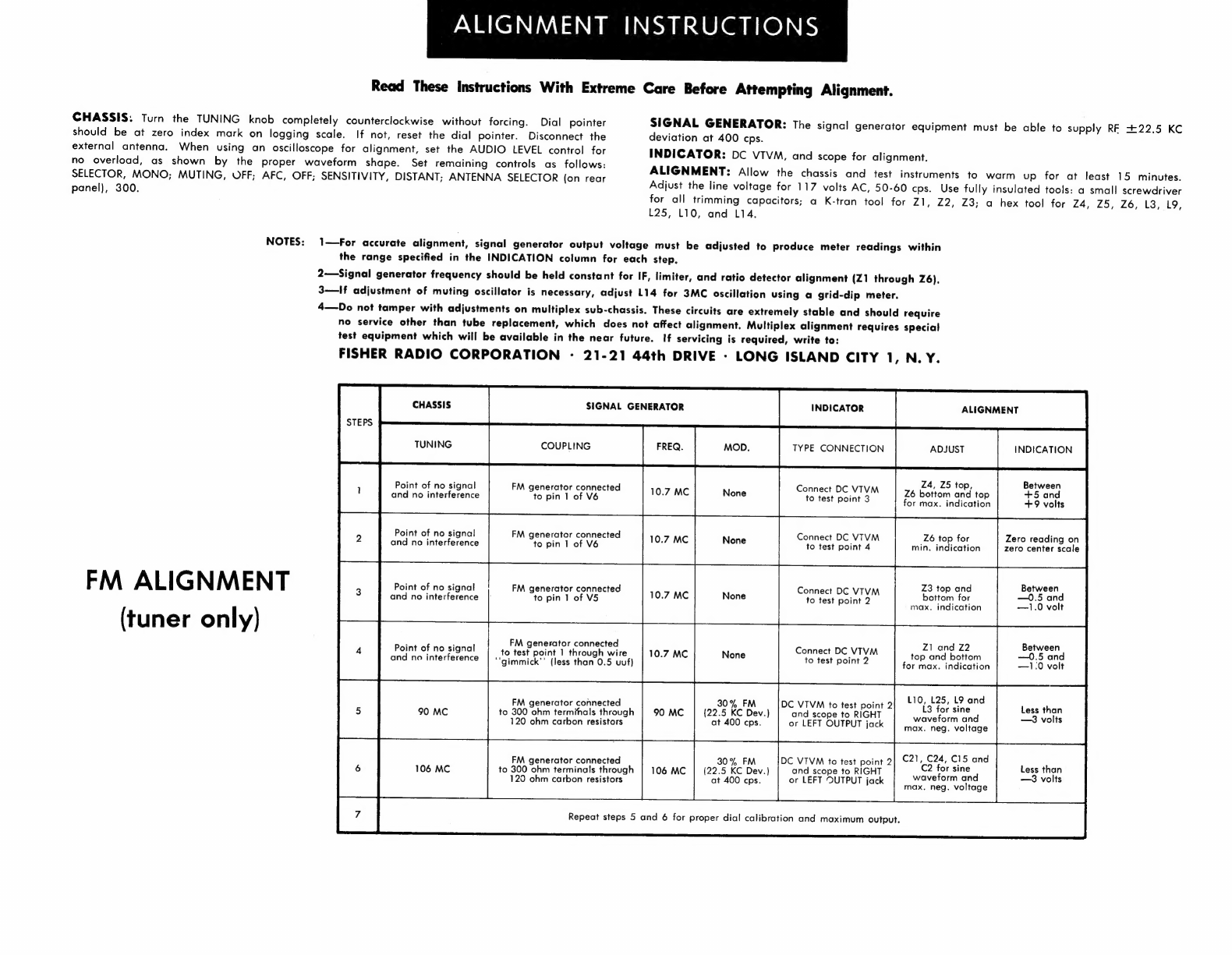
ALIGNMENT
INSTRUCTIONS
Read
These
Instructions
With
Extreme
Care
Before
Attempting
Alignment.
CHASSIS:
Turn
the
TUNING
knob
completely
counterclockwise
without
forcing.
Dial
pointer
SIGNAL
GENERATOR:
The
signal
generator
equipment
must
be
able
to
supply
RF
+22.5
KC
should
be
at
zero
index
mark
on
logging
scale.
If
not,
reset
the
dial
pointer.
Disconnect
the
deviation
at
400
cps.
external
antenna.
When
using
an
oscilloscope
for
alignment,
set
the
AUDIO
LEVEL
control
for
INDICATOR:
DC
VTVM,
and
scope
for
alignment.
no
overload,
as
shown
by
the
proper
waveform
shape.
Set
remaining
controls
as
follows:
ALIGNMENT
;
,
:
T:
All
th
:
SELECTOR,
MONO;
MUTING,
OFF;
AFC,
OFF;
SENSITIVITY,
DISTANT;
ANTENNA
SELECTOR
(on
rear
MG
betas
hes
See
ke
ee
Phare,
pate
eis
panel],
300.
just
the
line
voltage
for
volts
,
50-60
cps.
Use
fully
insulated
tools:
a
small
screwdriver
for
all
trimming
capacitors;
a
K-tran
tool
for
Z1, Z2,
Z3;
a
hex
tool
for
Z4,
Z5,
Z6,
L3,
L9,
L25,
L10,
and
L14.
NOTES:
1—For
accurate
alignment,
signal
generator
output
voltage
must
be
adjusted
to
produce
meter
readings
within
the
range
specified
in
the
INDICATION
column
for
each
step,
2—Signal
generator
frequency
should
be
held
constant
for
IF,
limiter,
and
ratio
detector
alignment
(Z1
through
Z6).
3-—If
adjustment
of
muting
oscillator
is
necessary,
adjust
L14
for
3MC
oscillation
using
a
grid-dip
meter.
4—Do
not
tamper
with
adjustments
on
multiplex
sub-chassis.
These
circuits
are
extremely
stable
and
should
require
no
service
other
than
tube
replacement,
which
does
not
affect
alignment.
Multiplex
alignment
requires
special
test
equipment
which
will
be
available
in
the
near
future.
If
servicing
is
required,
write
to:
FISHER
RADIO
CORPORATION
-
21-21
44th
DRIVE
-
LONG
ISLAND
CITY
1,
N.Y.
INDICATOR
ALIGNMENT
TYPE
CONNECTION
SIGNAL
GENERATOR
STEPS
|
cuss
TUNING
COUPLING
FREQ.
MOD.
Point
of
no
signal
and
no
interference
ADJUST
INDICATION
Z4,
Z5
top,
Z6
bottom
and
top
for
max.
indication
Between
+5
and
+9
volts
FM
generator
connected
to
pin
1
of
V6
Connect
DC
VIVM
to
test
point
3
Point
of
no
signal
FM
generator
connected
and
no
interference
Connect
DC
VTVM
to
pin
1
of
V6
to
test
point
4
Z6
top
for
Zero
reading
on
min.
indication
zero
center
scale
FM
ALIGNMENT
(tuner
only)
i
i
Between
Point
of
no
signal
FM
generator
connected
Connect
DC
VIVM
Z3
top
and
and
no
interference
to
pin
1
of
V5
to
test
point
2
bottom
for
—0.5
and
max.
indication
—1.0
volt
F :
FM
generator
connected
Z1
and
Z2
Between
Point
of
no
panel
to
test
point
1
through
wire
ecnnedt.
pets
top
and
bottom
—0.5
and
and
no
interference
‘'gimmick’’
(less
than
0.5
uuf)
O-TeettPoUn
for
max.
indication
—1:0
volt
L10,
L25,
L9
and
L3
for
sine
waveform
and
max.
neg.
voltage
FM
generator
connected
to
300
ohm
terminals
through
120
ohm
carbon
resistors
30%
FM
{22.5
KC
Dev.)
at
400
cps.
DC
VTVM
to
test
point
2
and
scope
to
RIGHT
or
LEFT
OUTPUT
jack
Less
than
90
MC
—3
volts
106
MC
90
MC
106
MC
C21,
C24,
C15
and
FM
generator
connected
30%
FM
DC
VTVM
to
test
point
2
.
to
300
ohm
terminals
through
(22.5
KC
Dev.)
and
scope
to
RIGHT
C2
ba
sine
4
ir
nen
120
ohm
carbon
resistors
at
400
cps.
or
LEFT
OUTPUT
jack
waveform
an
—3
volts
max.
neg.
voltage
Repeat
steps
5
and
6
for
proper
dial
calibration
and
maximum
output.

SCHEMATIC
DIAGRAM
!
|
cls
|
L?
|
v4
v2
EF94/6AU6
|
6cw4
Zi
L9
Las
9
pone
ey
|
a
|
.
.
Bev
[2
|
i
c24
|
L413
i
ee
*
56K
|
cis
|
c3-B]
C20
23
C3
-
ceo
|
ic
ce
;
a;
10
8
ns
mt
28
a
|
L509-139
RIO
=
Nee
ee
eet
330K
o027UF
T
|
R4 R6
=
100K
120
0.68
UH
{-
wore
IL
Ror
Sfx
h
22k
T
R36
|
|
cs
AAA
1000
|
8M
SI-A
|
=
————
SECTION
|
FRONT
|
|
|
R27
——-
-_—+
|
1oK
cRI
Le
|
6-88C20
1.2uH
|
C6
clo
$3
1000
t/t
t—IIl
1000
|
cla
SECTION
|
FRONT
1600
IF
zie
rake
oe
abl
|
ta
es
a
8
te,
=o
oes
az,
:
a!
R39
SI-A
a
470K
SECTION
|
REAR
R7
a
4
6°
3!
fo)
\
IM
C4
L
1
cao
RS
“T
.02UF
°
°
470K
:
°
to]
i
4
°
©.
R3
82
cll
25UF
T
$3
SECTION
|
REAR
ANTENNA
ane
a
aeetiss
ANTENNA
Paar
:
SELECTOR
+
SWITCH
200v
I75V:
148v
Oe
:
S
\wor
:
R20
R22
R24
wom
AN
>
B
°o
Oo
270
270
3.3K
omne)
105=120
VOLTS
AC
c28-8
c2e-c_L
c2e-p
50-60
CYCLES
40UF
Al
40UF
li
40UF
tk
ANTENNA
4 4
4
72
z - =
C46
ce
RI2
O1UF
820K
abi?
Sug
_3L2t
_3]L2
SWITCH
POSITIONS
SI
$2
$3
$4
$5
ANTENNA
MUTING
AC
@
SENSITIVITY
SELECTOR
AFC
CONTROL
SELECTOR
IPOWER
OFF
(SHOWN)
|
300
OHMS
(SHOWN)
|
OFF
(SHOWN)
OFF
(SHOWN)
MONO
(SHOWN)
C3
5000°T
c3a]
cas]
c38
er:
5000]
5000]
5000
1
LOCAL
72
OHMS
MICROTUNE
ON
STEREO
MONO
AUTOMATIC
DISTANT
AFC
|
STEREO
FILTER
AFC
2
Oi
ECF80/6BL8
Wiad

.oo27uF
647K
——t--=e=
+
27,00
TEST
POINT
MPX
$5
CONNECTIONS
=
SECTION
|
FRONT
;
SECTION
|
FRONT
R39
470K
R65
470K
an
v9
*
ECC88/6DJ8
SEE
NOTE
3
ue
83
SECTION
|
REAR
SECTION
|
REAR
ley
oO!
OUTPUT
A
LEFT
RBO
1
VIO
IM
=
ECCB8I/IZAT7
NOTES:
Sai
>)
DENOTES
READINGS
OF
MICROTUNE
CIRCUIT
oo
RIGHT
____
WHEN
IN
OPERATION.
Ber
|
fer
2.)
__
T
DENOTES
READINGS
OF
MUTING
CONTROL
Trcror]
[main]
:
ees
L
re
WHEN
SET
AT
MAXIMUM
POSITION
rao}
cso]
390
22M
3.-l4V
READING
WHILE
RECEIVING
AN
MPX
STEREO
li
STATION
ONLY.
C66
R63
Vil
R79
AUF
3
RB!
+
680
100K
IM
a
ECC8I/I2AT7
=
AW
#
2010
P9I14
SCHEMATIC
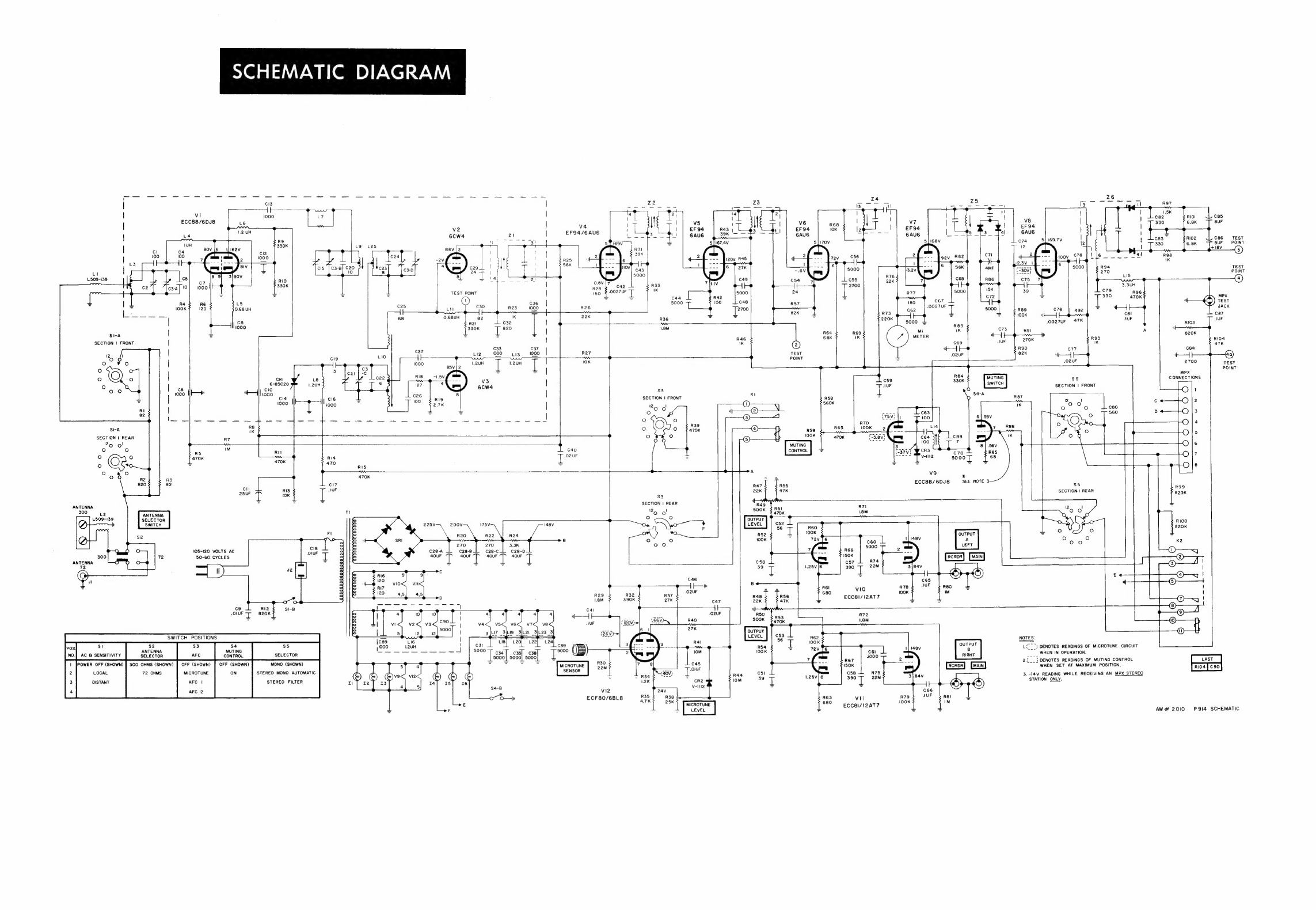
SCHEMATIC
DIAGRAM
v4
EF94/6AU6
L4
er
|
|
vl
1000
37.
|
ECC88/6DJ8
:
|
‘<
sev
[2
i
c24
!
|
ileal
-
|
c2
.
cis
|
c3-p]
C20
3
4
C3-D
L
509-139
RIO
2
330K
|
Ra R6
100k
120
0.68
UH
|
ca
.0027UF
947K
liooo
SI-A
|
=
|
SECTION
1
FRONT
|
|
R27
——
|
10k
2700
POINT
MPX
|
CRI
la
S5
CONNECTIONS
|
G-9SC20
1.2UH
SECTION
|
FRONT
c6
clo
s3
1000
YH
t—Hll
1000
|
cl4
SECTION
|
FRONT
1600
IF
in
a,
[2S
nae
ee)
ns
Op
enn,
Le
oe
at
pes
F
J
SI-A
Re
SECTION
|
REAR
ae
T
29
o!
oe———_—
° °
IM
+
cao
R5
"T
.02uUF
°
°
470K
R14
+
470
i
°
to
:
Ris
fo)
ee
v9
°
470K
*
Be
BG
ECC8B/6DU8
—SEE_NOTE
3
si
cil
AUF
25UF
—
[
SECTION
|
REAR
83
=
ia
=
SECTION
|
REAR
ANTENNA
oe
L2
ANTENNA
au
L509-139
SELECTOR
SWITCH
14ev
FI
R24
OUTPUT
AAA
>B
A
3.3K
LEFT
105-120
VOLTS
AC
28-8
c28-c
C28-D
300
72
50-60
CYCLES
aa
eT
40UF
T
40UF
al;
[RcRor]
ANTENNA
+ +
4
ae
72
=
2
z
=
mC
RI6
9 9
120
rT
vlo
vit
=
RI7
VIO
R80
=
120
45
4,5,
IM
>
-
>D
ECC8I/I2AT?
ce
Rize:
gicp.
CU
eee
ee
el
I
.O1UF
820K
1
t
1
|
|
|
vl
|
v4
V5<
V6
|
]
3[ui7
39
Sfi2t
32
SWITCH
POSITIONS
|
arr
aa
aaeD
St
32
33
$4
35
:
!
c3t
c39
oureus
}
DENOTES
READINGS
OF
MICROTUNE
CIRCUIT
ANTENNA
MUTING
5000
5000
AC
&
SENSITIVITY
SELECTOR
AFC
CONTROL
SELECTOR
Ls
steel
are:
a
RIGHT
____
WHEN
IN
OPERATION.
=
a
R67
|
2.;__
|
DENOTES
READINGS
OF
MUTING
CONTROL
POWER
OFF
(SHOWN)
|
300
OHMS
(SHOWN)
|
OFF
(SHOWN)
[|
OFF
(SHOWN)
MONO
(SHOWN)
150K
L
WHEN
SET
AT
MAXIMUM
POSITION,
Pros}
cso}
LOCAL
72
OHMS
MICROTUNE
ON
STEREO
MONO
AUTOMATIC
cs8
R75
3.-l4V
READING
WHILE
RECEIVING
AN
MPX
STEREO
390
22M
STATION
ONLY.
DISTANT
AFC
|
STEREO
FILTER
Ul
ut
ONLY’
AFC
2
vi2
ceé
On
ECF80/6BL8
ak
pi
Vtl
ie
alu
:
Rei
1
ECC8I/12AT7
=
AW#
2010
P9I14
SCHEMATIC

MPX
CONNECTIONS
MPX
INPUT
45°
HEATER
PINS
9
+125
VOLTS
+160
VOLTS
TUNING
INDICATOR
CHANNEL
A
OUTPUT
CHANNEL
B
OUTPUT
C209
C
2l6
+001
UF
NOTE
VOLTAGES
M
NO
SIGNAL
|

SCHEMATIC
DIAGRAM
«©
MULTIPLEX
SECTION
R202
15K
C
216
R
209
T.S.R
[102
|
2
a
c
210
1*
an
Ba
C22
_
R222
R224
MAF
T.S.R
[10
ee
yes
sas
and
OO!
LF
C225
i.
LUA
Mis
Ria
94V
94V
L102
[
ea
com
|
Rees
R225
vlio2
=
22K
=
22K
ECC8Il
6
\
C2
C222
R214
l2AT?
ang
.047KF
OS
SaLe
Reale
R
216
33K
lO
M
01
NOTE
LAST
VOLTAGES
MEASURED
WITH
VTVM
TO
CHASSIS
R230
|
C226
NO
SIGNAL
AT
MPX
INPUT.
.
MPX
SEPARATION
CONTROL
AW#1957B
P926WX
SCHEMATIC

MPX
INPUT
4,5
°
HEATER
PINS
9
+125
VOLTS
+160
VOLTS
TUNING
INDICATOR
CHANNEL
A
OUTPUT
MPX
CONNECTIONS
CHANNEL
B
OUTPUT
C209
SCHEMATIC
DIAGRAM
-
MULTIPLEX
SECTION
C
216
R
209
T.S.R
+001
ALF
33K
Y
4:
Rei?
4
R2ig8
C210
I8k
18K
NAF
T.S.R
O
Miu
R213
pa
100
K
|
100K
7
2
ss
es
:
2005
UF
ew
R2l2
R
216
33K
IO
M
NOTE
VOLTAGES
MEASURED
WITH
VTVM
TO
CHASSIS
NO
SIGNAL
AT
MPX
INPUT.
MPX
SEPARATION
CONTROL
C2el
R222
R224
097
UF
22K
22k
C223
OO1
LF
C225
L102
ome
R223
R225
=
22K
=
22K
LAST
AW#1957B
P926WX
SCHEMATIC

PARTS
DESCRIPTION
LIST
-
CAPACITORS
10%
tolerance
for
all
fixed
capacitors,
unless
otherwise
noted
or
marked
GMV
(guaranteed
minimum
value}.
All
capacitors
not
marked
uf
are
pF
(uuf).
Symbol
Description
Part
No.
C200
Ceramic,
.Oluf,
+80
—-20%,
500V
C50089-7
C201
Ceramic,
680,
1000V
C50072-2
C203
Ceramic,
220,
1000V
C50183-3
C204
Mica,
470,5%,
300V
C50332-4
C205
Ceramic,
82,
N1500,
1000V
C50070-7
C206
Ceramic,
.OOluf,
GMV,
500V
C50089-2
C207
Ceramic,
.005uf,
+80
—20%,
500V
C50089-6
C208,
209
Mica,
4700,5%,
500V
C50332-5
C210
Electrolytic,
luf,
350V
C€50283-3
C211,
212
Ceramic,
.0OOluf,
GMV,
500V
C50089-2
C213
Ceramic,
.O5uf,
+80
—-20%,
100V
C50073-2
C214
Mylar,
.0047uf,
400V
C50197-25
C215
Mica,
3900,5%,
500V
C50332-6
C216,
217
Ceramic,
.0Oluf,
GMV,
500V
C50089-2
C218
Ceramic,
.0O05uf,
20%
,
500V
C50089-1
C219
Ceramic,
330,
1000V
C50072-1
C220
Ceramic,
.0O05uf,
20%,
500V
C50089-1
C221,
222
Mylar,
.047uf,
10%,
250V
C50197-52
C223,
224
Ceramic,
.0O0luf,
1000V
C50072-3
C225,
226
Ceramic,
2200,
1000V
C50072-5
Symbol
R200
RESISTORS
AND
POTENTIOMETERS
In
ohms,
10%
tolerance,
¥
watt,
unless
otherwise
noted.
K=Kilohm,
M=Megohm.
Description
Composition,
22M
Part
No.
RC20BF226K
MULTIPLEX
SECTION
R201
Composition,
4.7K,
5%
R202
Composition,
15K,
5%
R203
Composition,
1OM
R204
Dep.
Carbon,
1M,
5%,
%3W
R205
Dep.
Carbon,
330K,5%,
¥sW
R206
Dep.
Carbon,
IM,
5%,
“3W
R207
Dep.
Carbon,
1.5M,
5%,
¥3W
R208
Dep.
Carbon,
22K,5%,
¥3W
R209,
210,
211,212
Composition,
33K,
5%
R213,
214
Dep.
Carbon,
100K,5%,
%3W
R215
Potentiometer,
50K,
MPX-separation
R216
Composition,
10M
R217,
218
Dep.
Carbon,
18K,5%,
%3W
R219,
220
Dep.
Carbon,
15K,5%,
%sW
R221
Composition,
}1OM
R222,
223,
224,225
Dep.
Carbon,
22K,5%,
¥3W
R226,
227,
—
228, 229,
230
Dep.
Carbon,
1M,5%,
%W
MISCELLANEOUS
Symbol
Description
CR100,
101,
102,
103
Diode,
Type
1112
L100
Coil,
Low
Pass
L101
Coil,
5.25
M.H.,5%
L102,103
Coil,
20M.H.,5%
Z100
Transformer,
19Ke
Z101
Coil,
38Ke
LAYOUT
MICROTUNE
AMP
ECF80
MIXER
Osc
|
V2
RF
AMP
GOLDEN
CASCODE
ANTENNA
CONNECTIONS.
INS-
103
tOW
PASS
AND
19KC
AMP
AUDIO
AMP
12AT7
ECC81
©
MPX
TEST
JACK
STEREO
BEACON
AMP
AND
MUTING
OSC
6DJ8/ECC88
38KC
SYNCH
OSC
3RD
IF
AMP
1ST
LIMITER
6AU6
EF94
2ND
LIMITER
DYNAMIC
LIMITER
Gv
8
6CW4
1ST
IF
AMP
2ND
IF
AMP
6AU6
EF94
LEFT
OUTPUT
AMP
12AT7
ECC81
©
RIGHT
OUTPUT
AMP
RC20BF472J
RC20BF153J
RC20BF106K
R33DC105J
R33DC334J
R33DC105J
R33DC155J
R33DC223J
RC20BF333J
R33DC104J
R50150-4
RC20BF106K
R33DC183J
R33DC153J
RC20BF106K
R33DC223J
R12DC105)
Part
No.
V-1112
L50210-30
150334-1
L50334-2
ZZ50210-34
2Z50210-33

FRONT-END
ADJUSTMENTS
FRONT-END
TEST
POINT
1
BOTTOM
COVER
PLATE
=
1ST
F©)
O
INS
117
FISHER
RADIO
CORPORATION
-
NEW
YORK
NOLH-104
©
1962
FISHER
RADIO
CORPORATION
PRINTED
IN
U.S.A.
398-W124C~-12
Table of contents


