THine CEL THCV231 User manual

THCV231_THCV236_Rev.2.30_E
Copyright©2016 THine Electronics, Inc.
THine Electronics, Inc.
1/56
Security E
THCV231 and THCV236
SerDes transmitter and receiver with bi-directional transceiver
General Description
The THCV231 and THCV236 are designed to
support video data transmission between the host and
display.
THCV231
One high-speed lane can carry up to 14bits data at a
pixel clock frequency from 12MHz to 160MHz.
THCV236
One high-speed lane can carry up to 32bit data and
3bits of synchronizing signals at a pixel clock
frequency from 6MHz to 160MHz by converting
RGB444 to YCbCr422.
The chipset, which has one high-speed data lane,
can transmit video data up to 1080p/60Hz.
The maximum serial data rate is 4.00Gbps/lane.
Features
Data width selectable
Wide frequency range
AC coupling for high-speed lanes
CDR requires no external frequency reference
Wide range supply voltage from 1.7V to 3.6V
Additional spread spectrum on data stream
2-wire serial interface bridge function(400kbps)
Remote side GPIO control and monitoring
THCV231
QFN32 (5mm x 5mm) with exposed pad ground
THCV236
QFN64 (9mm x 9mm) with exposed pad ground
EU RoHS compliant
Block Diagram
THCV236
CDR
Controls
Formatter
YCbCr to RGB
D31-D0
HSYNC
VSYNC
DE
CLKOUT
Settings
2-wire I/F
SDA/SCL
RXP
RXN
Deserializer
RCMP
RCMN
LVCMOS output
THCV231
LVCMOS input
PLL
Controls
Formatter
D11-D0
HSYNC
VSYNC
CLKIN
Settings
2-wire I/F
SDA/SCL
TXP
TXN
Serializer
OSC
TCMP
TCMN
LDO
OSC
LDO
CAPOUT
CAPINA
CAPINP
CAPOUT
CAPINA

THCV231_THCV236_Rev.2.30_E
Copyright©2016 THine Electronics, Inc.
THine Electronics, Inc.
2/56
Security E
Contents Page
General Description .............................................................................................................................................. 1
Features .................................................................................................................................................................. 1
Block Diagram ....................................................................................................................................................... 1
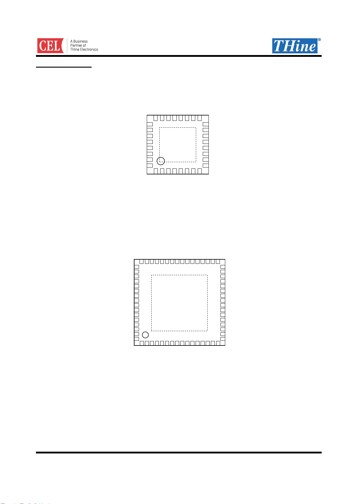
Pin Configuration .................................................................................................................................................. 3
Pin Description ...................................................................................................................................................... 4
Functional Overview ............................................................................................................................................. 9
Functional Description .......................................................................................................................................... 9
Internal Reference Output/Input Function (CAPOUT, CAPINA, CAPINP) .............................................. 9
Power Down (PDN1, PDN0, PDN) ................................................................................................................. 10
Pre-emphasis and Drive Select Function (THCV231 only) ......................................................................... 10
Permanent Clock Output (THCV236 only) .................................................................................................. 10
Spread Spectrum Clock Generator (SSCG) .................................................................................................. 11
Hot-Plug Function ........................................................................................................................................... 13
Lock Detect Function ...................................................................................................................................... 13
Field BET Operation ....................................................................................................................................... 14
Data Width and Frequency Range Select Function ..................................................................................... 16
Data Mapping .................................................................................................................................................. 16
2-wire serial I/F Mode ..................................................................................................................................... 17
2-wire serial I/F Device ID setting ................................................................................................................ 17
2-wire serial I/F Clock Stretching ................................................................................................................. 17
Read/Write access to Sub-Link Master Register ........................................................................................... 19
Read/Write access to Sub-Link Slave Register ............................................................................................. 20
Read/Write access to remote side 2-wire serial slave devices connected to Sub-Link Slave Device ............ 22
GPIO .............................................................................................................................................................. 26
Interruption .................................................................................................................................................... 28
Register Map ........................................................................................................................................................ 29
Absolute Maximum Ratings ............................................................................................................................... 38
Recommended Operating Conditions ................................................................................................................ 38
Electrical Specification ........................................................................................................................................ 38
AC Timing Diagrams and Test Circuits ............................................................................................................ 44
PCB Layout Guideline regarding VDD andAVDD for THCV236 ................................................................. 53
Package ................................................................................................................................................................. 54
Notices and Requests ........................................................................................................................................... 56

THCV231_THCV236_Rev.2.30_E
Copyright©2016 THine Electronics, Inc.
THine Electronics, Inc.
3/56
Security E
Pin Configuration
THCV236 (QFN 64pin)
PDN0
D27
1
PDN1
2
LFSEL
3
TEST1
4
TEST2
5
RF/BETOUT
6
COL0/INT/GPIO2
7
COL1/SD0
8
OUTSEL/SD1
9
TTLDRV/SD2/AIN0/GPIO1
10
LATEN/SD3/AIN1/GPIO0
11
D31
12
D30
13
D29
14
D28
15
VDD
17
18
D26
D25/GPIO4
19
20
D24/GPIO3
D23
21
22
D22
D21
23
24
D20
VDD
25
26
CLKOUT
D19
27
28
D18
D17
29
30
D16
D15
31
32
VDD
34
33
D14
36
35
D11
D12
38
37
D9
D10
40
39
AVDD
D8
42
41
D7
VDD
44
43
D5
D6
46
45
D3
D4
47
VSYNC
D2
52
51
50
49
D1
DE
HSYNC
VDD
56
55
54
53
CAPOUT
LOCKN/MSSEL
HTPDN/SUBMODE
D0
60
59
58
57
MAINMODE/RCMN
CAPINA
RXP
RXN
64
63
62
61
BET
OE
HFSEL/RCMP
16
48
(TOP VIEW)
65 EXPGND
D13
RXDEFSEL
PDN
D0
1
TEST1
2
TEST2
3
RF/BETOUT
4
SDA
5
SCL
6
GPIO3
7
GPIO4
8
9
10
D1
D2
11
12
D3
CLKIN
13
14
D4
D5
15
16
VDD
18
17
D7
20
19
D8
22
21
D10
23
VSYNC
D11
28
27
26
25
TCMN
TCMP
CAPOUT
HSYNC
32
31
30
29
CAPINA
TXP
THCV231 (QFN 32pin)
24
(TOP VIEW)
33 EXPGND
TXN
CAPINP
AVDD
D9
D6

THCV231_THCV236_Rev.2.30_E
Copyright©2016 THine Electronics, Inc.
THine Electronics, Inc.
4/56
Security E
Pin Description
Pin Description for THCV231
Pin Name
Pin No.
Type
Description
TXP
29
CO
High-Speed CML Signal Output (Main-Link)
TXN
30
CO
High-Speed CML Signal Output (Main-Link)
TCMP
27
CB
CML Signal Bidirectional Input/Output (Sub-Link)
TCMN
28
CB
CML Signal Bidirectional Input/Output (Sub-Link)
GPIO4
8
B
GPIO4 : General Purpose Input/Output.
When GPIO4 is used as Open-Drain Output, it must be
connected with a pull-up resistor to VDD.
When GPIO4 is used as push pull output, no external
component is required.
LATEN : Latch select input under Field BET (Sub-Link)
0 : Forbidden
1 : Latched result
GPIO3
7
B
GPIO3 : General Purpose Input/Output.
When GPIO3 is used as Open-Drain Output, it must be
connected with a pull-up resistor to VDD.
When GPIO3 is used as push pull output, no external
component is required.
SCL
6
B
SCL input/output for 2-wire serial I/F.
SDA
5
B
SDA input/output for 2-wire serial I/F.
CLKIN
13
I
Clock Input
D11-D0
23,22,20-17,15,14,12-9
I
Pixel Data Input
HSYNC
25
I
HSYNC Input
VSYNC
24
I
VSYNC Input
RF/BETOUT
4
B
RF : Input Clock Triggering edge select. See Figure 15.
0 : Falling Edge
1 : Rising Edge
BETOUT : Field BET Result Output when Field BET
mode.
PDN
1
IL
Power Down
0 : Power Down
1 : Normal Operation
TEST2
3
I
Test pin. Must be tied to Ground for normal operation.
TEST1
2
IL
Test pin. Must be tied to Ground for normal operation.
CAPOUT
26
PWR
Decoupling Capacitor Pin, 1.2V output.
CAPINA
31
PWR
Reference Input for Analog Circuit. Must be tied to
CAPOUT.
CAPINP
32
PWR
Reference Input for Analog Circuit. Must be tied to
CAPOUT.
VDD
16
PWR
1.7-3.6V Digital Power Supply Pin for LVCMOS I/O
AVDD
21
PWR
1.7-3.6V Analog Power Supply Pin for LDO
EXPGND
33
GND
Exposed Pad Ground. Must be tied to the PCB ground
plane through an array of vias.
CO : CML Output buffer , CB : CML Bi-directional buffer
I : LVCMOS Input buffer , IL : Low Speed LVCMOS Input buffer , B : LVCMOS Bi-directional buffer
PWR : Power supply , GND : Ground

THCV231_THCV236_Rev.2.30_E
Copyright©2016 THine Electronics, Inc.
THine Electronics, Inc.
5/56
Security E
Pin Description for THCV236
Pin Name
Pin No.
Type
Description
RXP
58
CI
High-Speed CML Signal Input(Main-Link)
RXN
57
CI
High-Speed CML Signal Input(Main-Link)
HFSEL/RCMP
61
CB/I
HFSEL : High Frequency Mode select when PDN1=0.
0 : High Frequency Mode Disable
1 : High Frequency Mode Enable
RCMP : CML Signal Bi-directional Input/Output(Sub-Link) when
PDN1=1.
MAINMODE/
RCMN
60
CB/I
MAINMODE : Setting V-by-One® HS Mode or Sync Free Mode
when PDN1=0
0 : V-by-One® HS Mode
1 : Sync Free Mode
RCMN : CML Signal Bi-directional Input/Output(Sub-Link)
when PDN1=1.
HTPDN/
SUBMODE
54
BO
HTPDN : Hot Plug Detect Output when PDN1=0. Must be
connected to Tx HTPDN with 10kΩ pull-up resistor.
SUBMODE : Sub-Link Mode Select when PDN1=1.
0 : 2-wire serial I/F Mode (default No Clock Stretching mode)
1 : Low Speed Data Bridge Mode
Forbid setting 1 when connecting with THCV231.
LOCKN/
MSSEL
55
BO
LOCKN : Lock Detect Output when PDN1=0. Must be connected
to Tx LOCKN with 10kΩ pull-up resistor.
MSSEL : Sub-Link Master/Slave Select when PDN1=1.
0 : Sub-Link Master side(inside 2-wire serial I/F is slave)
1 : Sub-Link Slave side(inside 2-wire serial I/F is master)
Sub-Link Master is connected to HOST MPU.
Forbid setting 1 when connecting with THCV231.
LATEN/SD3/
AIN1/GPIO0
11
B
LATEN : Latch select input under Field BET(Main-Link or
Sub-Link).
0 : NOT Latched result
1 : Latched result
SD3 : Sub-Link Data Input/Output when PDN1=1 and
SUBMODE=1.
When Sub-Link is Master (MSSEL=0), SD3 is output.
When Sub-Link is Slave (MSSEL=1), SD3 is input.
AIN1 : Device ID setting for 2-wire serial I/F when
SUBMODE=0 and MSSEL=0. See Table 18.
GPIO0 : General Purpose Input/Output when SUBMODE=0 and
MSSEL=1.
When GPIO0 is used as Open-Drain Output, it must be connected
with a pull-up resistor to VDD.
When GPIO0 is used as push pull output or input, no external
component is required.

THCV231_THCV236_Rev.2.30_E
Copyright©2016 THine Electronics, Inc.
THine Electronics, Inc.
6/56
Security E
TTLDRV/SD2/
AIN0/GPIO1
10
B
TTLDRV : LVCMOS Output Drive Strength Select when
PDN1=0.
0 : Weak Drive Strength
1 : Normal Drive Strength
SD2 : Sub-Link Data Input/Output when PDN1=1 and
SUBMODE=1.
When Sub-Link is Master (MSSEL=0), SD2 is input.
When Sub-Link is Slave (MSSEL=1), SD2 is output.
AIN0 : Device ID setting for 2-wire serial I/F when
SUBMODE=0 and MSSEL=0. See Table 18.
GPIO1 : General Purpose Input/Output when SUBMODE=0 and
MSSEL=1.
When GPIO1 is used as Open-Drain Output, it must be connected
with a pull-up resistor to VDD.
When GPIO1 is used as push pull output or input, no external
component is required.
OUTSEL/SD1
9
B
OUTSEL : Permanent Clock Output Enable when PDN1=0.
0 : Permanent Clock Output Disable
1 : Permanent Clock Output Enable
SD1 : Sub-Link Data Input/Output when PDN1=1.
When SUBMODE=0, SD1 is used as SCL input/output for 2-wire
serial I/F, requires pull-up resistor to VDD.
When SUBMODE=1 and MSSEL=0, SD1 is input.
When SUBMODE=1 and MSSEL=1, SD1 is output.
COL1/SD0
8
B
COL1 : Color Space Converter Enable when PDN1=0 and
MAINMODE=0.
0 : Color Space Converter Disable
1 : Color Space Converter Enable
Data Width Setting when PDN1=0 and MAINMODE=1. See
Table 15.
SD0 : Sub-Link Data Input/Output when PDN1=1.
When SUBMODE=0, SD0 is used as SDA input/output for 2-wire
serial I/F, requires pull-up resistor to VDD.
When SUBMODE=1 and MSSEL=0, SD0 is input.
When SUBMODE=1 and MSSEL=1, SD0 is output.
COL0/INT/
GPIO2
7
B
COL0 : Data Width Setting when PDN1=0. See Table 15.
INT : Interrupt signal output for Sub-Link when SUBMODE=0
and MSSEL=0. It must be connected with a pull-up resistor to
VDD.
L : Interrupt occurred
H : Steady state
GPIO2 : General Purpose Input/Output when SUBMODE=0 and
MSSEL=1.
When GPIO2 is used as Open-Drain Output, it must be connected
with a pull-up resistor to VDD.
When GPIO2 is used as push pull output or input, no external
component is required.
CLKOUT
26
O
Clock Output
D31-D26
12-15,17,18
O
Pixel Data Output

THCV231_THCV236_Rev.2.30_E
Copyright©2016 THine Electronics, Inc.
THine Electronics, Inc.
7/56
Security E
D25/GPIO4
19
B
D25 : Pixel Data Output
GPIO4 : General Purpose Input/Output when SUBMODE=0,
MSSEL=1 and RXDEFSEL=0.
When GPIO4 is used as Open-Drain Output, it must be connected
with a pull-up resistor to VDD. When GPIO4 is used as push pull
output or input, no external component is required.
D24/GPIO3
20
B
D24 : Pixel Data Output
GPIO3 : General Purpose Input/Output when SUBMODE=0,
MSSEL=1 and RXDEFSEL=0.
When GPIO3 is used as Open-Drain Output, it must be connected
with a pull-up resistor to VDD. When GPIO3 is used as push pull
output or input, no external component is required.
D23-D0
21-24,27-31,33-39,
42-47,52,53
O
Pixel Data Output
DE
51
O
DE Output
HSYNC
50
O
HSYNC Output
VSYNC
48
O
VSYNC Output
OE
63
IL
Output Enable
0 : LVCMOS Output Disable (Hi-Z) except for HTPDN,
LOCKN when PDN1=0 and except for BETOUT when BET=1
1 : LVCMOS Output Enable
BET
64
IL
Field BET entry
0 : Normal Operation
1 : Field BET Operation
RF/BETOUT
6
B
RF : Output Clock Triggering edge select. See Figure 16.
0 : Falling Edge
1 : Rising Edge
BETOUT : Field BET Result Output
RXDEFSEL
62
I
Internal Register Default Setting Select. See Table 35, Table 36
0 : for THCV231
1 : for THCV235
LFSEL
3
I
Low Frequency mode select
0 : Low Frequency mode Disable
1 : Low Frequency mode Enable
Forbid setting 1 when connecting with THCV231.
PDN1
2
IL
Sub-Link Power Down
0 : Power Down. Main-Link setting by external pin
1 : Normal Operation. Main-Link Setting by 2-wire serial I/F
PDN0
1
IL
Main-Link Power Down
0 : Power Down
1 : Normal Operation
TEST2
5
I
Test pin. Must be tied to Ground for normal operation.
TEST1
4
IL
Test pin. Must be tied to Ground for normal operation.
CAPOUT
56
PWR
Decoupling Capacitor Pin, 1.2V output.
CAPINA
59
PWR
Reference Input for Analog Circuit. Must be tied to CAPOUT.
VDD
49,41,32,25,16
PWR
1.7-3.6V Digital Power Supply Pin for LVCMOS I/O
AVDD
40
PWR
1.7-3.6V Analog Power Supply Pin for LDO
EXPGND
65
GND
Exposed Pad Ground. Must be tied to the PCB ground plane
through an array of vias.
CI : CML Input buffer , CB : CML Bi-directional buffer
I : LVCMOS Input buffer , IL : Low Speed LVCMOS Input buffer , O: LVCMOS Output buffer
B : LVCMOS Bi-directional buffer , BO : Open-Drain LVCMOS Bi-directional buffer
PWR : Power supply , GND : Ground

THCV231_THCV236_Rev.2.30_E
Copyright©2016 THine Electronics, Inc.
THine Electronics, Inc.
8/56
Security E
Table 1. Pin Sharing Description (THCV231-THCV236 usage)
Sub-Link State →
2-wire serial
I/F Mode
Sub-Link
Master/Slave →
Master
PDN1
1
HTPDN/SUBMODE
0
LOCKN/MSSEL
0
BET
0
RXDEFSEL
0
RF/BETOUT
RF
BETOUT(*1)
COL0/INT/GPIO2
INT
COL1/SD0
SD0(SDA)
OUTSEL/SD1
SD1(SCL)
TTLDRV/SD2/AIN0/GPIO1
AIN0
LATEN/SD3/AIN1/GPIO0
AIN1
LATEN(*2)
D24/GPIO3
GPIO3(*3)
D25/GPIO4
GPIO4(*3)
HTPDN/SUBMODE
SUBMODE
LOCKN/MSSEL
MSSEL
MAINMODE/RCMN
RCMN
HFSEL/RCMP
RCMP
*1 When Field BET mode (Main-Link or Sub-Link), it functions as BETOUT output.
*2 When Field BET mode (Main-Link or Sub-Link), it functions as LATEN input.
*3 Through GPIO input is default on register setting

THCV231_THCV236_Rev.2.30_E
Copyright©2016 THine Electronics, Inc.
THine Electronics, Inc.
9/56
Security E
Functional Overview
With High Speed CML SerDes, proprietary encoding scheme and CDR (Clock and Data Recovery)
architecture, the THCV231 and THCV236 enable transmission of 14bit data through Main-Link by single
differential pair cable with minimal external components. In addition, the THCV231 and THCV236 have
Sub-Link which enables bi-directional transmission of 2-wire serial interface signals, GPIO signals and also
HTPDN/LOCKN signals for Main-Link through the other 1-pair of CML-Line. It does not need any external
frequency reference such as a crystal oscillator. The THCV231 - THCV236 system is able to watch peripheral
devices and to control them via 2-wire serial interface or GPIOs. They also can report interrupt events caused by
change of GPIO inputs and internal statuses.
Functional Description
Internal Reference Output/Input Function (CAPOUT, CAPINA, CAPINP)
An internal regulator produces the 1.2V (CAPOUT). This 1.2V linear regulator can’t supply any other
external loads. Bypass CAPOUT to GND with 10uF.
CAPINP (THCV231 only) supplies reference voltage for internal PLL, and CAPINA supplies reference
voltage for any internal analog circuit. Bypass CAPINP/CAPINA to GND with 0.1uF to remove high frequency
noise. CAPOUT, CAPINA and CAPINP must be tied together.
Power supply AVDD is supposed to be stabilized with de-coupling capacitor and series noise filter (for example,
ferrite bead).
CAPOUT
CAPINA
CAPINP
THCV231
10uF
0.1uF
0.1uF
AVDD
Power
Supply
CAPOUT
CAPINA
THCV236
10uF
0.1uF
AVDD
Power
Supply
Figure 1. Connection of CAPOUT, CAPINA, CAPINP and Decoupling Capacitor

THCV231_THCV236_Rev.2.30_E
Copyright©2016 THine Electronics, Inc.
THine Electronics, Inc.
10/56
Security E
Power Down (PDN1, PDN0, PDN)
PDN1, PDN0 and PDN turn off internal circuitry of Main-Link and Sub-Link separately.
Table 2. Power Down Setting(THCV231)
PDN
Operation
0
Both Main-Link and Sub-Link power down
1
Both Main-Link and Sub-Link active
Table 3. Power Down Setting(THCV236)
PDN1
PDN0
Operation
0
0
Both Main-Link and Sub-Link power down
0
1
Only Main-Link is active
1
0
Only Sub-Link is active
1
1
Both Main-Link and Sub-Link active
Pre-emphasis and Drive Select Function (THCV231 only)
Pre-emphasis can equalize severe signal degradation caused by long-distance or high-speed transmission. PRE
register selects the strength of pre-emphasis. CMLDRV register controls CML Main-Link output swing level.
See Table 4.
Table 4. Pre-emphasis and Drive Select function table
CMLDRV[1:0]
(register)
PRE
(register)
Condition
Swing Level
Pre-emphasis Level
00
0
400mV diff p-p
0dB
1
6dB
01
0
600mV diff p-p
0dB
1
3.5dB
10
*
800mV diff p-p
0dB
11
*
Forbidden
Permanent Clock Output (THCV236 only)
When there is no input from Main-Link, the THCV236 will output internal oscillator clock from CLKOUT pin.
This function is controlled by OUTSEL pin or OUTSEL_ENABLE register and OUTSEL_SETTING register.
See Table 5.
Table 5. Permanent Clock Output function table (PDN1=1)
OUTSEL_
ENABLE
(register)
OUTSEL_
SETTING
(register)
Output Clock
Frequency(*1)
0
*
-
1
00
80MHz
01
40MHz(default)
10
20MHz
11
10MHz
*1 typical value

THCV231_THCV236_Rev.2.30_E
Copyright©2016 THine Electronics, Inc.
THine Electronics, Inc.
11/56
Security E
Spread Spectrum Clock Generator (SSCG)
The THCV231 serial data output and the THCV236 parallel data and clock outputs are modulated by
programmable SSCG. The THCV231 and THCV236 SSCG are enabled by only SSEN register. The modulation
rate and modulation frequency variation of output spread is controlled through the SSCG control registers on
each device. Do not enable spread spectrum for both the THCV231 and THCV236 at the same time.
Table 6. SSCG enable signal
Mode Entry Signal
Description
SSEN(register)
0:SSCG Disable
1:SSCG Enable
When customer use the mode and frequency range shown in Table 7, register setting is required according to
Table 8.
Table 7. Main-Link mode and frequency range requiring register setting
Mode Setting
Freq.Range[MHz]
(SSCG Enable)
Register
Setting
(*2)
MAINMODE
HFSEL
COL1
COL0
min
max
1
0
0
0
26.6
40
Case1
1
0
0
1
26.6
50
Case1
1
0
1
0
33.3
66.6
Case2
1
1
(*1)
(*1)
50
100
Case3
*1 Don’t care
*2 See Table 8
Table 8. SSCG register setting
Step
Register Address(HEX)
Register Value(HEX)
Description
Sub-Link
Master side
Sub-Link
Slave side
Case1
Case2
Case3
THCV231
THCV236
1
0x70
0xF0
0x01
Set 1 to PLL_SET_EN
2
0x76
0xF6
0x02
0x02
0x01
Set PLL_SET0
3
0x78
0xF8
0x3C
0x30
0x20
Set PLL_SET1
4
0x7C
0xFC
0x35
0x34
0x24
Set PLL_SET2
Modulation frequency fmod can be determined by HFSEL and LFSEL settings, input clock frequency and
FMOD register setting (default value 0xD). Refer to following formula.
FMOD
f
fCLKSSCG
128
mod
fCLKSSCG is the frequency listed in Table 9 and Table 10.

THCV231_THCV236_Rev.2.30_E
Copyright©2016 THine Electronics, Inc.
THine Electronics, Inc.
12/56
Security E
Table 9. fCLKSSCG (THCV231)
HFSEL
(register)
fCLKSSCG
0
(1/tTCIP)/2
1
(1/tTCIP)/4
Table 10. fCLKSSCG (THCV236)
HFSEL
LFSEL
fCLKSSCG
0
0
(1/tRCP)/2
1
0
(1/tRCP)/4
*
1
Forbidden Setting
Up to 0.5 % spread at the 30kHz modulation frequency is stable for most cases. In case of using out of this
range, please verify at the actual system.

THCV231_THCV236_Rev.2.30_E
Copyright©2016 THine Electronics, Inc.
THine Electronics, Inc.
13/56
Security E
Hot-Plug Function
HTPDN signal indicates connecting condition between the Transmitter and the Receiver. HTPDN of the
transmitter side is high when the Receiver is not active or not connected. Then the Transmitter can enter into the
power down mode. HTPDN is set to low by the Receiver when the Receiver is active and connects to the
Transmitter, and then the Transmitter must start up and transmit CDR training pattern for link training.
HTPDN is transferred to the Transmitter via Sub-Link line. HOST MPU can confirm HTPDN state by reading
Sub-Link Master register (0x00 bit0 HTPDN).
Lock Detect Function
LOCKN indicates whether the receiver CDR PLL is in the lock state or not. LOCKN at the Transmitter input is
set to High when the Receiver is not active or at the CDR PLL training state. LOCKN is set to low by the
Receiver when CDR lock is done. Then the CDR training mode finishes and the Transmitter shifts to the normal
operation.
LOCKN is transferred via Sub-Link line. HOST MPU can confirm LOCKN state by reading Sub-Link Master
register (0x00 bit1 LOCKN).
2-wire
serial
Slave
V-by-One
®
HS
Main-Link
Receiver
Main-Link
LOCKN,
HTPDN
LOCKN,
HTPDN
Sub-Link Block
(Master
)
Sub-Link
THCV236
Sub-Link
Master
Register
0x00
bit1:LOCKN
bit0:HTPDN
V-by-One
®
HS
Main-Link
Transmitter
2-wire
serial
Master
Sub-Link
Slave
Register
THCV231
Sub-Link Block
(Slave
)
Host
MPU
SD1(SCL)
SD0(SDA)
THCV231:Sub-Link Slave, THCV236:Sub-Link Master
Figure 2. HTPDN, LOCKN transmission route

THCV231_THCV236_Rev.2.30_E
Copyright©2016 THine Electronics, Inc.
THine Electronics, Inc.
14/56
Security E
Field BET Operation
In order to help users to check validity of CML serial line (Main-Link and Sub-Link), the THCV231 and
THCV236 have an operation mode in which they act as a bit error tester (BET). In Main-Link Field BET mode,
the THCV231 internally generates a test pattern which is then serialized onto the Main-Link CML line. The
THCV236 also has BET function mode. The THCV236 receives the data stream and checks bit errors. The
generated data pattern is then 8b/10b encoded, scrambled, and serialized onto the CML channel. As for the
THCV236, the internal test pattern check circuit gets enabled and reports result on a certain pin named BETOUT.
In Sub-Link Field BET mode, Sub-Link Master device internally generates test pattern which is then serialized
onto the Sub-Link CML line. Sub-Link Slave device also has BET function mode. Sub-Link Slave device
receives the data stream and checks bit errors. Note that Sub-Link Slave device must be set this mode prior to
Sub-Link Master device. Pattern check result is output from BETOUT pin of the Sub-Link Slave device. The
BETOUT pin goes LOW whenever bit errors occur, or it stays HIGH when there is no bit error.
In Main-Link Field BET mode, user can select two kinds of check result, latched result or NOT latched result
by setting LATEN pin input. The latched result is reset by setting LATEN=0. In Sub-Link Field BET mode, only
latched result is available. In order to reset the latched result, please once turn off the power and entry Sub-Link
Field BET from power on sequence.
GPIO4 pin (THCV231) and LATEN/SD3/AIN1/GPIO0 pin (THCV236) function as LATEN in Field BET
mode (Main-Link or Sub-Link).
It is not possible to realize Main-Link Field BET and Sub-Link Field BET at the same time.
Table 11. Main-Link Field BET Operation Settings
THCV231/236
Common Setting
THCV236
Setting
Condition
PDN0/PDN1/PDN
SUBMODE
BET
BET_SEL
LATEN
Main-Link
Sub-Link
Output Latch
Select
1
0
1
(*1)
0
(*2)
0
Field BET
Operation
Normal
Operation
NOT Latched Result
1
Latched Result
*1 THCV231: Register setting (0x53 bit1), THCV236: Pin setting
*2 Register setting (0x53 bit0, Default 0)
Table 12. THCV236 Main-Link Field BET Result
BETOUT
Output
L
Bit Error Occurred
H
No Error

THCV231_THCV236_Rev.2.30_E
Copyright©2016 THine Electronics, Inc.
THine Electronics, Inc.
15/56
Security E
Table 13. Sub-Link Field BET Operation Setting
THCV231/THCV236
Common Setting
THCV231
Setting
THCV236
Setting
Condition
BET
BET_SEL
PDN
GPIO3
GPIO4
PDN1
MSSEL
LATEN
Sub-Link
Output
Latch
Select
1
(*1)
1
(*2)
1
0
-
1
1
1
(*3)
Field BET
Operation
(THCV231→THCV236)
Latched
Result
1
1
(*3)
0
-
Field BET
Operation
(THCV236→THCV231)
*1 THCV231: Register setting (0x53 bit1), THCV236: Pin setting. Note that BET pin should be 0 at power on sequence.
*2 Register setting (0x53 bit0, Default 0)
*3 Forbidden 0 setting
Table 14. Sub-Link Slave device Sub-Link Field BET Result
BETOUT
Output
L
Bit Error Occurred
H
No Error
THCV231 THCV236
CLKIN
BET=1
(Register)
Test Pattern
Checker
Test Pattern
Generator
Data inputs
are ignored
RF/BETOUT
Test Point
for
Field BET
LATEN/SD3/AIN1/GPIO0 = 0 or 1
BET_SEL=0
(Register)
BET=1
(Pin)
BET_SEL=0
(Register)
0
1
Main-Link
Figure 3. Main-Link Field BET Configuration
THCV231 THCV236
Test Pattern
Checker
Test Pattern
Generator RF/BETOUT
Test Point
for
Field BET
OSC
BET=1
(Register)
BET_SEL=1
(Register)
LATEN/SD3/AIN1/GPIO0 =1
BET=1
(Pin)
BET_SEL=1
(Register)
Sub-Link
THCV236THCV231
Test Pattern
Checker
Test Pattern
Generator
RF/BETOUT
Test Point
for
Field BET
OSC
BET=1
(Register)
BET_SEL=1
(Register)
GPIO4=1 BET=1
(Pin)
BET_SEL=1
(Register)
Sub-Link
Figure 4. Sub-Link Field BET Configuration

THCV231_THCV236_Rev.2.30_E
Copyright©2016 THine Electronics, Inc.
THine Electronics, Inc.
16/56
Security E
Data Width and Frequency Range Select Function
The THCV231 and THCV236 support a variety of data width and frequency range. Frequency range is
different depending on the mode setting SSCG enable and disable setting. Refer to Table 15 for details.
Table 15. Main-Link Operation Mode Select
Mode Setting
Freq.Range
[MHz]
Main-Link
CML
Bit Rate
Data Width
Comment
SSCG
Disable
SSCG
Enable (*1)
MAINMODE
HFSEL
COL1
COL0
min
max
min
max
0
*
*
*
-
-
-
-
-
-
Forbidden
1
0
0
0
12
30
26.6
60
x50
14
-
1
0
0
1
15
40
26.6
75
x40
14
-
1
0
1
0
20
75
33.3
100
x30
14
-
1
0
1
1
-
-
-
-
-
-
Forbidden
1
1
0
0
-
-
-
-
-
-
Forbidden
1
1
0
1
50
70
50
70
x20
14
(*2)
70
160
70
160
-
1
1
1
0
50
70
50
70
x15
10
(*2)
70
160
70
160
-
1
1
1
1
-
-
-
-
-
-
Forbidden
*1 Note that register setting is required depending on the mode setting and used frequency range. See Table 7.
*2 Register setting is required. See Table 16.
Table 16. Register setting (HFSEL=1 and Frequency range is from 50MHz to 70MHz)
Step
Register Address(HEX)
Register Value(HEX)
Description
Sub-Link
Master side
Sub-Link
Slave side
THCV231
THCV236
1
0x70
0xF0
0x01
Set 1 to PLL_SET_EN
2
0x76
0xF6
0x02
0x01
Set PLL_SET0
3
0x78
0xF8
0x20
Set PLL_SET1
4
0x7C
0xFC
0x24
Set PLL_SET2
Data Mapping
Table 17. Data Mapping
MAINMODE
0
1
1
1
1
1
1
1
1
HFSEL
*
0
0
0
0
1
1
1
1
COL1
*
0
0
1
1
0
0
1
1
COL0
*
0
1
0
1
0
1
0
1
D0
-
D0
D0
D0
-
-
D0/RAW4
D0/YC0
-
D1
-
D1
D1
D1
-
-
D1/RAW5
D1/YC1
-
D2
-
D2
D2
D2
-
-
D2/RAW6
D2/YC2
-
D3
-
D3
D3
D3
-
-
D3/RAW7
D3/YC3
-
D4
-
D4
D4
D4
-
-
D4/RAW8
D4/YC4
-
D5
-
D5
D5
D5
-
-
D5/RAW9
D5/YC5
-
D6
-
D6
D6
D6
-
-
D6/RAW10
D6/YC6
-
D7
-
D7
D7
D7
-
-
D7/RAW11
D7/YC7
-
D8
-
D8
D8
D8
-
-
D8/RAW0
-
-
D9
-
D9
D9
D9
-
-
D9/RAW1
-
-
D10
-
D10
D10
D10
-
-
D10/RAW2
-
-
D11
-
D11
D11
D11
-
-
D11/RAW3
-
-
HSYNC(*1)
-
HSYNC
HSYNC
HSYNC
-
-
HSYNC
HSYNC
-
VSYNC(*1)
-
VSYNC
VSYNC
VSYNC
-
-
VSYNC
VSYNC
-
*1 Any signal as well as sync signal can be transmitted.

THCV231_THCV236_Rev.2.30_E
Copyright©2016 THine Electronics, Inc.
THine Electronics, Inc.
17/56
Security E
Sub-Link Mode Setting
2-wire serial I/F Mode
2-wire serial I/F Mode enables register access, using GPIO (General Purpose Input/Output) pin and interrupt
function. Sub-Link Master device has 2-wire serial slave block and can be connected to HOST MPU, Sub-Link
Slave device has 2-wire serial master block and can be connected to remote side 2-wire serial slave devices.
HOST MPU can access register of Sub-Link Master device, Sub-Link Slave device and remote side 2-wire
serial slave devices.
2-wire serial I/F Device ID setting
AIN1 and AIN0 pins determine Device ID setting of the THCV236. Only Sub-Link Master device has AIN1
and AIN0 pin. AIN1 and AIN0 choose one of 4 addresses which give an identification address to the THCV236
under 2-wire serial interface bus topology.
Table 18. 2-wire serial I/F Device ID select (Sub-Link Master device Only)
AIN1
AIN0
Device ID
0
0
0x0B
0
1
0x34
1
0
0x77
1
1
0x65
2-wire serial I/F Clock Stretching
In principle, when Sub-Link bridges 2-wire serial interface communication from Sub-Link Master to Sub-Link
Slave or remote side 2-wire serial slave devices, time lag occurs between HOST MPU side 2-wire serial access
and Sub-Link Slave internal bus access or remote side 2-wire serial access.
2WIRE_MODE (Sub-Link Master side register, 0x0F bit1-0) selects whether 2-wire serial slave of Sub-Link
Master perform clock stretching or not.
When 2WIRE_MODE = 00, Sub-Link Master device wait HOST MPU until Sub-Link Slave register access or
remote side 2-wire serial slave register access is completed by clock stretching.
When 2WIRE_MODE = 01, Sub-Link Master device informs HOST MPU that Sub-Link Slave register access
or remote side 2-wire serial register access has been completed by interruption (INT pin) without clock
stretching.

THCV231_THCV236_Rev.2.30_E
Copyright©2016 THine Electronics, Inc.
THine Electronics, Inc.
18/56
Security E
Write 1
to 0x25 or 0x26 or 0x2B or 0x2C A
...
SD1
(SCL)
SD0
(SDA)
Access start to Sub-Link Slave’s register or
Remote side 2-wire serial Slave’s register
...
Stop
Condition
Write 1
to 0x25 or 0x26 or 0x2B or 0x2C A
...
SD1
(SCL)
SD0
(SDA)
Access start to Sub-Link Slave’s register or
Remote side 2-wire serial Slave’s register
...
Stop
Condition
Clock Stretching
INT
Interruption
2WIRE_MODE=00 (Clock Stretching Mode)
2WIRE_MODE=01 (No Clock Stretching Mode)
Sub-Link communication time + Sub-Link Slave side internal bus access process time
or
Sub-Link communication time + Remote side 2-wire serial Access Time
Sub-Link Slave register Access or
Remote side 2-wire serial register
Access completion
Figure 5. 2WIRE_MODE Operation

THCV231_THCV236_Rev.2.30_E
Copyright©2016 THine Electronics, Inc.
THine Electronics, Inc.
19/56
Security E
Read/Write access to Sub-Link Master Register
HOST MPU can directly access Sub-Link Master’s register by 2-wire serial I/F.
Register address of Sub-Link Master is from 0x00 to 0x7F. See Register Map for more information.
Sub-Link
Master
Sub-Link Master Device
Sub-Link Block
Register
(Address
0x00 – 0x7F)
2-wire
Slave
Host
MPU
SD1(SCL)
LOCKN/MSSEL=0AIN1,AIN0 = User Select
SD0(SDA)
Figure 6. Host to Sub-Link Master Register access configuration
S Register addressDevice ID W A A Write data #1 A ... A P
S
P
A
A
W
Start condition
Stop condition
ACK
NACK
Write command indicator
Access from 2-wire serial interface Master
Access from 2-wire serial interface Slave
Figure 7. 2-wire serial I/F write to Sub-Link Master register protocol
S Register addressDevice ID W A A Read data #1 A ... PDevice ID R ASr A
S
P
A
A
W
R
Start condition
Stop condition
ACK
NACK
Read command indicator
Write command indicator
Access from 2-wire serial interface Master
Access from 2-wire serial interface Slave
Repeated start condition
Sr
Figure 8. 2-wire serial I/F read to Sub-Link Master register protocol

THCV231_THCV236_Rev.2.30_E
Copyright©2016 THine Electronics, Inc.
THine Electronics, Inc.
20/56
Security E
Read/Write access to Sub-Link Slave Register
HOST MPU can access to Sub-Link Slave’s register via Sub-Link Master by Sub-Link Master register settings.
Register address of Sub-Link Slave is from 0x80 to 0xFF. See Register Map for more information.
Sub-Link Block
2-wire
Slave
Sub-Link
Master
Sub-Link Master DeviceSub-Link Slave Device
Sub-Link Block
Sub-Link
Slave
2-wire
Master
Sub-Link
line
LOCKN/MSSEL=0AIN1,AIN0 = User Select
Interrupt signal
Host
MPU
SD1(SCL)
SD0(SDA)
INT
Register
(Address
0x00 – 0x7F)
Register
(Address
0x80 – 0xFF)
Figure 9. Host MPU to Sub-Link Slave Register access configuration
Table 19. Sub-Link slave registerWrite Procedure
Step
Description
R/W
Address
1
Write 1 or 0 and clear(auto clear) access status register (2WIRE_ACS_END_INT).
W
0x02 bit7
2
Set the data for Sub-Link Slave to write (Max 16byte).
W
0x10-0x1F
3
Set Device ID of Sub-Link Master device.
(Value corresponding to AIN1 and AIN0 setting. e.g.[AIN1,AIN0]=[0,0] → 7’h0B)
W
0x20
4
Set the byte number written to Sub-Link Slave (Max 16byte).
(Byte number = register value + 1)
W
0x21
5
Set the start address of Sub-Link Slave register to write.
W
0x23
6
Write 1 to WR_START_8B. (Start write access to Sub-Link Slave register)
W
0x25 (*1)
7
(*2)
2-wire serial slave of Sub-Link Master perform clock stretching until Sub-Link Slave
register access is completed.
-
-
7
(*3)
When write access is completed, 2WIRE_ACS_END_INT register value become 1
and interrupt occurs (INT=H → L).
-
-
8
If write access was normally ended, read value should be “0x1”.
R
0x02 bit7
*1 It’s Prohibit that HOST MPU start access to Sub-Link Slave or remote 2-wire serial slave before the previous access to
Sub-Link Slave or remote side 2-wire serial slave is completed.
*2 When 2WIRE_MODE = 00 (Clock Stretching Mode)
*3 When 2WIRE_MODE = 01 (No Clock Stretching Mode)
This manual suits for next models
1
Table of contents
Other THine Transceiver manuals