THine THCS251 User manual

THCS251_Rev.3.01_E
Copyright©2023 THine Electronics, Inc. THine Electronics, Inc.
1/33
SC: E
THCS251
35-bits GPIO or high speed Bus signal Transceiver
General description
The THCS251 integrates Serializer and Deserializer
onto a single chip, which supports general purpose
input and output (GPIO) signals through two pairs of
differential signal.
GPIO sampling clock is selectable from external
reference clock or internal oscillator clock.
The 8B10B encoding and decoding adopted by
THCS251 is easy to connect to optical / wireless
communication devices with high robustness and DC
balanced signal.
The built-in adaptive equalizer enables flexible cable
selection.
Application
The THCS251 can applicable to any systems which
have many control signals between PCBs, for
example Multi-function printers, Amusement
machines, Factory Automation and TVs.
Features
Support up to 35-bits GPIO
Not required to input GPIO sampling clock in
internal oscillator clock mode
Full duplex communication by two pairs of
differential signal
Output buffer open-drain or push-pull selectable
Support up to 8-bits low speed GPIO in low
power Standby mode
Integrated adaptive equalizer for long or lossy
media
8B10B encoding and decoding
Configurable digital noise filter
Error detection and indication
External reference clock frequency: 9-100MHz
Spread Spectrum Clock Generator to reduce EMI
Operating single power supply voltage: 1.7 V -
3.6 V
Wide range IO voltage: 1.7V - 3.6V
Operating ambient temperature: -40°C to 85°C
Block diagram
LDO
GPIO
D0/D34
...
D34/D0
REFIN
REFOUT
TXP
TXN RXP
RXN
RXN
RXP TXN
TXP
GPIO
D34/D0
...
D0/D34
THCS251 (Master mode) THCS251 (Slave mode)
LVCMOS I/O
LDO
OSC SSCG PLL
Tx
(Serializer)
Formatter
Rx
(Deserializer)
LVCMOS I/O
OSCSSCG
PLL
Tx
(Serializer)
Formatter
Rx
(Deserializer)
REFEN

THCS251_Rev.3.01_E
Copyright©2023 THine Electronics, Inc. THine Electronics, Inc.
2/33
SC: E
Contents page
General description..................................................................................................................................................1
Application..............................................................................................................................................................1
Features ...................................................................................................................................................................1
Block diagram.........................................................................................................................................................1
1. Pin configuration.............................................................................................................................................3
2. Pin description.................................................................................................................................................4
3. Absolute maximum ratings..............................................................................................................................8
4. Recommended operating conditions ...............................................................................................................8
5. Electrical characteristics..................................................................................................................................9
5.1. Current consumption...............................................................................................................................9
5.2. LVCMOS/Analog input DC specifications ...........................................................................................10
5.3. LVCMOS AC characteristics................................................................................................................. 11
5.4. CML DC characteristics........................................................................................................................14
5.5. CMLAC characteristics ........................................................................................................................14
6. CML Line Eye diagrams ...............................................................................................................................19
6.1. CML output Eye diagrams.....................................................................................................................19
6.2. CML input Eye diagrams ......................................................................................................................20
7. Function.........................................................................................................................................................21
7.1. Functional overview..............................................................................................................................21
7.2. Power supply.........................................................................................................................................21
7.2.1. Internal regulator output/input function (CAPOUT, CAPINA, CAPINP) ....................................21
7.3. Operating mode.....................................................................................................................................21
7.4. Transmission mode................................................................................................................................22
7.4.1. Full duplex Bi-directional transmission mode...............................................................................22
7.4.2. Unidirectional transmission mode.................................................................................................24
7.5. IO configuration ....................................................................................................................................25
7.5.1. Input and Output digital noise filter ..............................................................................................25
7.5.2. LVCMOS output buffer type configuration...................................................................................25
7.5.3. 5V Tolerant I/O..............................................................................................................................25
7.6. Sampling clock configuration................................................................................................................26
7.6.1. Sampling clock selection...............................................................................................................26
7.6.2. Spread Spectrum Clock Generator (SSCG) and REFIN frequency...............................................28
7.7. Error detection and indication...............................................................................................................29
7.8. Standby mode........................................................................................................................................30
8. Package..........................................................................................................................................................31
Notices and Requests.............................................................................................................................................32

THCS251_Rev.3.01_E
Copyright©2023 THine Electronics, Inc. THine Electronics, Inc.
3/33
SC: E
1. Pin configuration
12 13 14
D9 / D25
VDD
D3 / D31
D4 / D30
D5 / D29
D6 / D28
D7 / D27
D8 / D26
RESERVED 63 18 D11 / D23
FILTSEL1 64 17 D10 / D24
123456
RESETN 62 19 D12 / D22
7 8 15 16
MSSEL
RF / OSCSEL0
READY
SSEN
FILTSEL0
D0 / D34
D1 / D33
D2 / D32
9 10 11
TEST1 61 20 D13 / D21
INT / LOCKN 60 21 D14 / D20
CAPINP 59 22 D15 / D19
TXP 58 23 D16 / D18
TXN 57 24 D17 / D17
CAPINA 56 25 VDD
RXN 55 26 REFIN / REFOUT/ OSCSEL1
RXP 54 27 D18 / D16
CAPOUT 53 28 D19 / D15
AVDD 52 29 D20 / D14
TEST2 51 30 D21 / D13
DATA_WIDTH 50 31 D22 / D12
OBUF 49 QFN-64 32 D23 / D11
36 35 34 3342 41 40 39 38 3748 47 46 45 44 43
D26 / D8
D25 / D9
VDD
D24 / D10
D32 / D2
D31 / D3
D30 / D4
D29 / D5
D28 / D6
D27 / D7
STANDBY
DIRSEL1
DIRSEL0
REFEN
D34 / D0
D33 / D1
(TOP VIEW)
65 EXPGND
THCS251_Rev.3.01_E
Copyright©2023 THine Electronics, Inc. THine Electronics, Inc.
4/33
SC: E
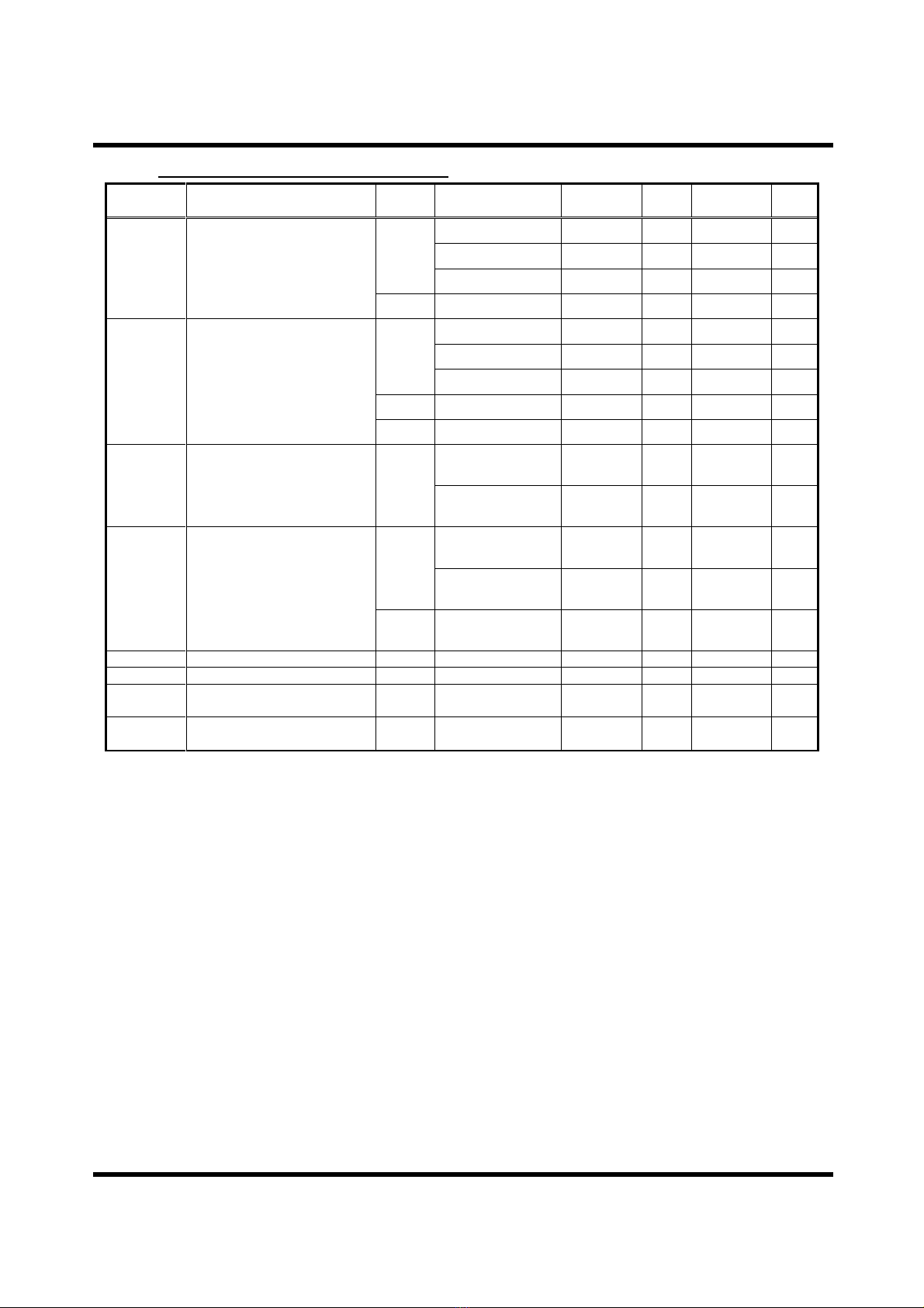
2. Pin description
P
in
Name
P
in
No.
Type
Description
Refere
nce
TXP 58 CO High-speed CML signal output -
TXN 57 CO High-speed CML signal output -
RXP 54 CI High-speed CML signal input -
RXN 55 CI High-speed CML signal input -
RESETN 62 IL Chip reset
0: Chip reset
1: Chip operation
-
STANDBY 48 IL Standby mode entry
0:Normal mode operation
1:Standby mode operation
-
RESERVED 63 IL RESERVED shall be tied to Ground. -
MSSEL 1 IL Master/Slave mode select
0: Master mode
1: Slave mode
-
FILTSEL1 64 IL FILTSEL1: digital noise filter select Table 5
DIRSEL0 46 IL DIRSEL0: GPIO direction select
Table 2
Table 4
DIRSEL1 47 IL DIRSEL1: GPIO direction select
Table 2
Table 4
OBUF 49 IL Output buffer type select
0: open-drain
1: push-pull
-
REFEN 45 IL
Data sampling clock select (Master mode)
0: Internal oscillator clock
1: External reference clock
-
CDR clock output enable (Slave mode)
0: REFOUT pin is Hi-Z state
1: CDR clock output from REFOUT pin
-
REFIN/
REFOUT/
OSCSEL1 26 B
REFIN: (Master mode) External Reference
clock input -
REFOUT: (Slave mode) CDR clock output -
OSCSEL1: (Master mode) Oscillator clock
frequency select Table 10
OSCSEL1: (Slave mode) Hi-Z -
DATA_WIDTH 50 IL GPIO Aggregator/Deaggregator data width
select
Table 2
Table 4
Table 14
RF/
OSCSEL0 2 IL
RF:(Master mode) input clock edge select Table 11
Figure 14
RF:(Slave mode) output clock edge select
OSCSEL0: (Master mode) Oscillator clock
frequency select Table 10

THCS251_Rev.3.01_E
Copyright©2023 THine Electronics, Inc. THine Electronics, Inc.
5/33
SC: E
P
in
Name
P
in
No.
Type
Description
Refere
nce
OSCSEL0: (Slave mode) Set to Low
D0/
D34 6 BT D0(Master mode): Data input -
D34(Slave mode): Data output
D1/
D33 7 BT D1(Master mode): Data input -
D33(Slave mode): Data output
D2/
D32 8 BT D2(Master mode): Data input -
D32(Slave mode): Data output -
D3/
D31 9 BT D3(Master mode): Data input -
D31(Slave mode): Data output -
D4/
D30 10 B D4(Master mode): Data input -
D30(Slave mode): Data output -
D5/
D29 11 B D5(Master mode): Data input -
D29(Slave mode): Data output -
D6/
D28 12 B D6(Master mode): Data input -
D28(Slave mode): Data output -
D7/
D27 13 B D7(Master mode): Data input -
D27(Slave mode): Data output -
D8/
D26 14 B D8(Master mode): Data input -
D26(Slave mode): Data output -
D9/
D25 15 B D9(Master mode): Data input -
D25(Slave mode): Data output -
D10/
D24 17 B D10(Master mode): Data input -
D24(Slave mode): Data output -
D11/
D23 18 B D11(Master mode): Data input -
D23(Slave mode): Data output -
D12/
D22 19 B D12(Master mode): Data input -
D22(Slave mode): Data output -
D13/
D21 20 B D13(Master mode): Data input -
D21(Slave mode): Data output -
D14/
D20 21 B D14(Master mode): Data input/output -
D20(Slave mode): Data input/output -
D15/
D19 22 B D15(Master mode): Data input/output -
D19(Slave mode): Data input/output -
D16/
D18 23 B D16(Master mode): Data input/output -
D18(Slave mode): Data input/output -
D17/
D17 24 B D17(Master mode): Data input/output -
D17(Slave mode): Data input/output -
D18/
D16 27 B D18(Master mode): Data input/output -
D16(Slave mode): Data input/output -
D19/
D15 28 B D19(Master mode): Data input/output -
D15(Slave mode): Data input/output -
D20/
D14 29 B D20(Master mode): Data input/output -
D14(Slave mode): Data input/output -
D21/
D13 30 B D21(Master mode): Data input/output -
D13(Slave mode): Data input/output -
D22/
D12 31 B D22(Master mode): Data input/output -
D12(Slave mode): Data input/output -
THCS251_Rev.3.01_E
Copyright©2023 THine Electronics, Inc. THine Electronics, Inc.
6/33
SC: E
P
in
Name
P
in
No.
Type
Description
Refere
nce
D23/
D11 32 B D23(Master mode): Data input/output -
D11(Slave mode): Data input/output -
D24/
D10 33 B D24(Master mode): Data input/output -
D10(Slave mode): Data input/output -
D25/
D9 35 B D25(Master mode): Data input/output -
D9(Slave mode): Data input/output -
D26/
D8 36 B D26(Master mode): Data input/output -
D8(Slave mode): Data input/output -
D27/
D7 37 B D27(Master mode): Data input/output -
D7(Slave mode): Data input/output -
D28/
D6 38 B D28(Master mode): Data input/output -
D6(Slave mode): Data input/output -
D29/
D5 39 B D29(Master mode): Data input/output -
D5(Slave mode): Data input/output -
D30/
D4 40 B D30(Master mode): Data input/output -
D4(Slave mode): Data input/output -
D31/
D3 41 BT D31(Master mode): Data input/output -
D3(Slave mode): Data input/output -
D32/
D2 42 BT D32(Master mode): Data input/output -
D2(Slave mode): Data input/output -
D33/
D1 43 BT D33(Master mode): Data input/output -
D1(Slave mode): Data input/output -
D34/
D0 44 BT D34(Master mode): Data input/output -
D0(Slave mode): Data input/output -
SSEN 4 BL
SSEN(Master mode): SSCG PLL enable
0: SSCG PLL is disabled
1: SSCG PLL is enabled
SSEN(Slave mode): Set to Low -
FILTSEL0 5 BL FILTSEL0: digital noise filter select Table 5
INT/
LOCKN 60 BO
INT: Interrupt output when READY=1
0: Error occurred
1(pull-up): No Error
-
LOCKN(Master mode): Lock detect input
0: Lock state
1(pull-up): Unlock state
-
LOCKN(Slave mode): Lock detect output
0: Lock state
1(pull-up): Unlock state
-
READY 3 B CML Link communication status
0: Unlock state
1: Lock state
-
TEST1 61 IL TEST1 shall be tied to Ground. -
TEST2 51 AI TEST2 shall be tied to Ground. -
CAPOUT 53 PWR Decoupling capacitor Pin, 1.2V output. Figure 9
CAPINA 56 PWR 1.2V Analog power supply input. Figure 9
THCS251_Rev.3.01_E
Copyright©2023 THine Electronics, Inc. THine Electronics, Inc.
7/33
SC: E
P
in
Name
P
in
No.
Type
Description
Refere
nce
CAPINP 59 PWR 1.2V Analog power supply input. Figure 9
VDD 16
25
34 PWR 1.7-3.6V Digital power supply input for
LVCMOS I/O. -
AVDD 52 PWR 1.7-3.6V Analog power supply input for on-
chip regulator. Figure 9
EXPGND 65 GND Exposed Pad Ground. Must be tied to the PCB
ground plane through an array of vias. -
Pin Type definition
Analog Buffer
CO : CML Output buffer
CI : CML Input buffer
AI : Analog Input buffer
LVCMOS buffer
IL : Low speed schmitt trigger LVCMOS Input buffer
B : LVCMOS Bi-directional buffer
BO : Open-drain LVCMOS Bi-directional buffer
BL : Low speed 5V tolerant schmitt trigger LVCMOS Bi-directional buffer
BT : Low speed 5V tolerant LVCMOS Bi-directional buffer
Power/Ground
PWR : Power supply
GND : Ground
THCS251_Rev.3.01_E
Copyright©2023 THine Electronics, Inc. THine Electronics, Inc.
8/33
SC: E
3. Absolute maximum ratings
Parameter
Min
Typ
Max
Unit
Supply voltage(VDD,AVDD) -0.3 - 4.0 V
LVCMOS input voltage -0.3 - VDD+0.3 V
LVCMOS output voltage -0.3 - VDD+0.3 V
5V tolerant Bi-directional buffer input voltage -0.3 - VDD+2.5 V
5V tolerant Bi-directional buffer output voltage -0.3 - VDD+2.5 V
Open-drain output voltage -0.3 - 4.0 V
CML receiver input voltage -0.3 - CAPINA+0.3 V
CML transmitter output voltage -0.3 - CAPINP+0.3 V
Output current -50 - 50 mA
Storage temperature -55 - 125 °C
Junction temperature - - 125 °C
Reflow peak temperature/time - - 260/10 °C/sec
Theta-ja (Junction-to-Ambient) 29.1 [*1] °C/W
Psi-jt (Junction-to-Top of Package) 1.1 [*1] °C/W
Maximum power dissipation @+25°C 3.4[*1] W
“Absolute maximum ratings” are those values beyond which the safety of the device cannot be guaranteed.
They are not meant to imply that the device should be operated at these limits. The tables of “Electrical
Characteristics” specify conditions for device operation.
*1: Thermal parameters are not guaranteed value. This value assists board and system level designers.
4. Recommended operating conditions
Parameter
Min
Typ
Max
Unit
Supply voltage(VDD,AVDD) 1.7 - 3.6 V
Operating ambient temperature -40 - 85 °C
VDD andAVDD supply voltage shall be the same voltage.

THCS251_Rev.3.01_E
Copyright©2023 THine Electronics, Inc. THine Electronics, Inc.
9/33
SC: E
5. Electrical characteristics
5.1. Current consumption
Symbol
Parameter
Pin
Type
Condition
Min
Typ
Max
Unit
Idd_w1 Normal mode current
Low current use case [*1] PWR AVDD=3.3V
VDD=3.3V - 80 - mA
Idd_w2 Normal mode current
High current use case [*2] PWR AVDD=3.3V
VDD=3.3V - 260 - mA
Idda_stby Standby mode current PWR AVDD=3.3V
VDD=3.3V - 4 - mA
Idda_slp Sleep mode current PWR AVDD=3.3V
VDD=3.3V - 3 - mA
Idda_rst Reset mode current PWR AVDD=3.3V
VDD=3.3V - 3 - mA
PWR : Power supply
*1: Master mode of Unidirectional transmission mode, 35-bits GPIO input, 80MHz of REFIN clock
*2: Slave mode of Unidirectional transmission mode, 35-bits GPIO output, 80MHz of REFOUT clock
THCS251_Rev.3.01_E
Copyright©2023 THine Electronics, Inc. THine Electronics, Inc.
10/33
SC: E
5.2. LVCMOS/Analog input DC specifications
Symbol
Parameter
Pin
Type
Condition
Min
Typ
Max
Unit
VIH High level input voltage B,BT,
BO
1.7V≦VDD<2.0V 0.65 VDD - VDD V
2.0V≦VDD<3.0V 0.70 VDD - VDD V
3.0V≦VDD≦3.6V 2.0 - VDD V
IL,BL 1.7V≦VDD≦3.6V 0.70 VDD - VDD V
VIL Low level input voltage
B,BT,
BO
1.7V≦VDD<2.0V 0 - 0.35 VDD V
2.0V≦VDD<3.0V 0 - 0.30 VDD V
3.0V≦VDD≦3.6V 0 - 0.8 V
IL,BL 1.7V≦VDD≦3.6V 0 - 0.30 VDD V
AI 1.7V≦VDD≦3.6V 0 - 0.15 VDD V
VOH High level output voltage B,BT,
BL
1.7V≦VDD<2.0V
IOH=-2mA VDD -
0.30 - VDD V
2.0V≦VDD≦3.6V
IOH=-4mA VDD -
0.45 - VDD V
VOL Low level output voltage
B,BT,
BL
1.7V≦VDD<2.0V
IOL=2mA 0 - 0.30 V
2.0V≦VDD≦3.6V
IOL=4mA 0 - 0.45 V
BO 1.7V≦VDD≦3.6V
IOL=2mA 0 - 0.27 V
IIH Input leak current high IL VIN=VDD -10 - 10 uA
IIL Input leak current low IL VIN=0V -10 - 10 uA
IOZH Output leak current high in
Hi-Z state B,BT,
BL,BO VIN=VDD -10 - 10 uA
IOZL Output leak current low in
Hi-Z state B,BT,
BL,BO VIN=0V -10 - 10 uA
AI : Analog Input buffer
IL : Low speed schmitt trigger LVCMOS Input buffer
B : LVCMOS Bi-directional buffer
BO : Open-drain LVCMOS Bi-directional buffer
BL : Low speed 5V tolerant schmitt trigger LVCMOS Bi-directional buffer
BT : Low speed 5V tolerant LVCMOS Bi-directional buffer
THCS251_Rev.3.01_E
Copyright©2023 THine Electronics, Inc. THine Electronics, Inc.
11/33
SC: E
5.3. LVCMOSAC characteristics
Symbol
Parameter
Condition
Min
Typ
Max
Unit
tRSN RESETN low time - 3 - - us
tTCIP REFIN period DATA_WIDTH=0 10 - 66.6 ns
DATA_WIDTH=1 12.5 - 111 ns
tTCH REFIN high time - 0.35 tTCIP 0.5 tTCIP 0.65 tTCIP ns
tTCL REFIN low time - 0.35 tTCIP 0.5 tTCIP 0.65 tTCIP ns
tTS Data input setup to REFIN
Pin type:
B 1.7V≦VDD≦3.6V 2.0 - - ns
Pin type:
BT
1.7V≦VDD<2.25V 25 - - ns
2.25V≦VDD≦2.75V 2.5 - - ns
2.75V<VDD≦3.6V 2.0 - - ns
tTH Data input hold to REFIN - 1.0 - - ns
tTPD Power on to RESETN high
delay - 0 - - ns
tOSC Internal oscillator clock
period
OSCSEL1=0
OSCSEL0=0 41.67 50 62.5 ns
OSCSEL1=1
OSCSEL0=0 20.84 25 31.25 ns
OSCSEL1=1
OSCSEL0=1 10.42 12.5 15.62 ns
tDCP Data sampling clock period REFEN=0 - tOSC - ns
REFEN=1 - tTCIP - ns
tFLTCK Noise filter clock period REFEN=0 10.42 12.5 15.62 ns
REFEN=1 - tTCIP - ns
tTCD Input data to output data
delay (Master mode to
Slave mode)
SSEN=0
FILTSEL1=0
FILTSEL0=0 12 tDCP - 25 tDCP ns
FILTSEL1=0
FILTSEL0=1 19 tDCP - 35 tDCP ns
FILTSEL1=1
FILTSEL0=0 24 tDCP - 43 tDCP ns
FILTSEL1=1
FILTSEL0=1 34 tDCP - 59 tDCP ns
SSEN=1
FILTSEL1=0
FILTSEL0=0 57 tDCP - 110 tDCP ns
FILTSEL1=0
FILTSEL0=1 64 tDCP - 120 tDCP ns
FILTSEL1=1
FILTSEL0=0 69 tDCP - 128 tDCP ns
FILTSEL1=1
FILTSEL0=1 79 tDCP - 144 tDCP ns
tRCP REFOUT period - - tDCP - ns
tRCH REFOUT high time - - 0.5 tDCP - ns
tRCL REFOUT low time - - 0.5 tDCP - ns
tDOUT Data output period - - tDCP - ns
tRS Data output setup to
REFOUT - 0.45 tDCP
- 0.675 - - ns
tRH Data output hold to
REFOUT - 0.45 tDCP
- 2.175 - - ns
tRCD Input data to output data
delay (Slave mode to Master
mode)
FILTSEL1=0
FILTSEL0=0 12 tDCP - 25 tDCP ns
FILTSEL1=0
FILTSEL0=1 19 tDCP - 35 tDCP ns
FILTSEL1=1
FILTSEL0=0 24 tDCP - 43 tDCP ns
FILTSEL1=1 34 tDCP - 59 tDCP ns
THCS251_Rev.3.01_E
Copyright©2023 THine Electronics, Inc. THine Electronics, Inc.
12/33
SC: E
Symbol
Parameter
Condition
Min
Typ
Max
Unit
FILTSEL0=1
tRRDY RESETN high to READY
high delay - 0 - 10 ms
tNRDY STANDBY low to READY
high delay - 0 - 10 ms
tSRDY STANDBY high to READY
high delay - 0 - 10 ms
tSSKW STANDBY high of Master
mode and Slave mode
skew margin - -400 - +400 us
tTLH Clock and Data output low
to high transition time
Clock - - 2.1 ns
Data(Pin type=B) - - 4.2 ns
Data(Pin type=BT) - - 5.9 ns
tTHL Clock and data output high
to low transition time
Clock - - 2.1 ns
Data(Pin type=B) - - 4.3 ns
Data(Pin type=BT) - - 6.1 ns
Figure 1 LVCMOS input timing diagram
VDD/2
VDD/2VDD/2
VDD/2 VDD/2
tTCIP
tTS tTH
tTCH(RF=0)
tTCL(RF=1)
RF=0
RF=1
D0-D34
REFIN
tTCL(RF=0)
tTCH(RF=1)
CL= 8pF
RD = 10Ω
Test Point
THCS251_Rev.3.01_E
Copyright©2023 THine Electronics, Inc. THine Electronics, Inc.
13/33
SC: E
Figure 2 LVCMOS output timing diagram
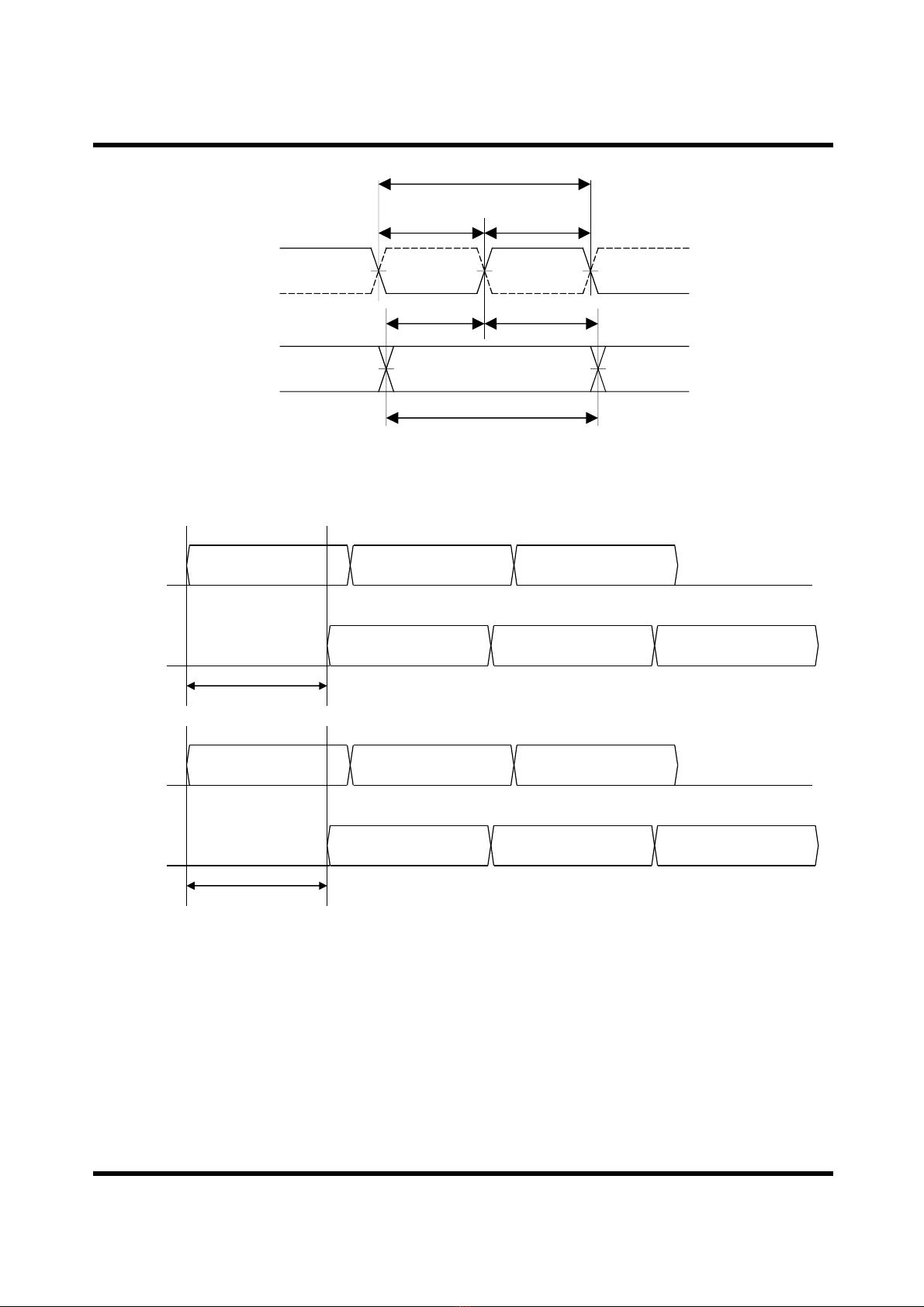
Figure 3 GPIO Input to Output delay timing diagram
VDD/2
VDD/2VDD/2
VDD/2 VDD/2
tRCP
tRS tRH
tRCH(RF=0)
tRCL(RF=1)
RF=0
RF=1
D34-D0
REFOUT
tRCL(RF=0)
tRCH(RF=1)
tDOUT
tTCD
Chip Master
mode Inputs
D0-D34 DATA1 DATA2 DATA3
DATA1 DATA2 DATA3
Chip Slave
mode Outputs
D34-D0
tRCD
DATA1 DATA2 DATA3
DATA1 DATA2 DATA3
Chip Slave
mode Inputs
D34-D0
Chip Master
mode Outputs
D0-D34
THCS251_Rev.3.01_E
Copyright©2023 THine Electronics, Inc. THine Electronics, Inc.
14/33
SC: E
5.4. CMLDC characteristics
Symbol
Parameter
Condition
Min
Typ
Max
Unit
VTOD CML differential output peak
to peak signal - 600 800 1000 mVpp
VTOC CML common mode output
voltage - - 1200 - 0.5
VTOD - mV
ITOH CML output leak current
high RESETN=0
TXP/N=CAPINA -30 - 30 uA
ITOS CML output short current RESETN=0
TXP/N=0V -80 - - mA
VRTH CML differential input high
threshold - - - 50 mV
VRTL CML differential input low
threshold - -50 - - mV
IRIH CML input leak current high RESETN=0
RXP/N=CAPINA -10 - 10 uA
IRIL CML input leak current low RESETN=0
RXP/N=0V -10 - 10 uA
IRRIH CML input current high RXP/N=CAPINA - - 2 mA
IRRIL CML input current low RXP/N=0V -6 - - mA
RRIN CML differential input
resistance - 80 100 120 Ω
5.5. CMLAC characteristics
Symbol
Parameter
Condition
Min
Typ
Max
Unit
tTRF CML output rise and fall time (20%-
80%) - 50 - 150 ps
tTPLL0 RESETN=1 to CML output delay - - - 10 ms
tTPLL1 RESETN=0 to CML output high fix
delay - - - 500 ns
tTNP0 READY low to training pattern output
delay - - - 100 us
tTBIT Output unit interval DATA_WIDTH=0 - tDCP÷30 - ns
DATA_WIDTH=1 - tDCP÷50 - ns
tRBIT Input unit interval - 250 - 2222 ps
tRPLL0 Training pattern input to LOCKN low
delay Unidirectional mode - - 10 ms
tRPLL1 RESETN low to LOCKN High delay Unidirectional mode - - 10 us
tRLCK0 LOCKN low to data output delay Unidirectional mode - - 5 ms

THCS251_Rev.3.01_E
Copyright©2023 THine Electronics, Inc. THine Electronics, Inc.
15/33
SC: E
Figure 4 CML outputAC characteristics diagram
Figure 5 CML buffer equivalent circuit
TXP
TXN
75~200nF
< 5mm
Vdiff = (TXP) - (TXN)
50Ω
50Ω
75~200nF
20%
80%
20%
80%
tTRF tTRF
TXP RXP
TXN RXN
Vbias
Zdiff=100ohm
C=75~
200nF
GND
THCS251 THCS251
CML Transmitter
CML Receiver
50Ω
CAPINP
C=75~
200nF
50Ω 50Ω
50Ω
THCS251_Rev.3.01_E
Copyright©2023 THine Electronics, Inc. THine Electronics, Inc.
16/33
SC: E
Figure 6 GPIO/CMLBi-directional mode Power on & Reset timing diagram
THCS251 (Chip Master mode)
Tx
(Master side)
Rx
(Master side)
REFIN
RESETNm
READYm
D0/D34m
D17/D17m
D18/D16m
D34/D0m
THCS251 (Chip Slave mode)
Rx
(Slave side)
Tx
(Slave side)
R
EFOUT
RESETNs
READY
s
D34/D0s
D17/D17s
D18/D16s
D0/D34s
TXm
TXs
DATA_WIDTH=0, DIRSEL1/0=00
tTPD
VDD
RESETNs
D18/D16s
D34/D0s
Valid Input
Invalid Input Invalid Input Valid Invalid Input
REFIN
tTPLL0
RESETNm
D18/D16m
D34/D0m
Valid Output Valid
Invalid Output Invalid
TXs
Training Normal
READYs
tRRDY
READYm
tTNP0
tTPLL1
TXm
Training Normal Training
Invalid Input
D0/D34m
D17/D17m Invalid Input Valid Input Valid Input Invalid Input
D34/D0s
D17/D17s
Invalid Output Valid Output Valid
REFOUT
Hi-Z
Invalid
clock
Invalid clock
Invalid clock
Invalid
Solid line : RF=0
Dashed line : RF=1
Hi-Z
Hi-Z
Hi
-
Z
Hi
-
Z
Hi
-
Z
THCS251_Rev.3.01_E
Copyright©2023 THine Electronics, Inc. THine Electronics, Inc.
17/33
SC: E
Figure 7 GPIO/CMLUnidirectional mode lock & unlock timing diagram
DIRSEL1/0=11
THCS251 (Chip Master mode)
Tx
(Master side)
Rx
(Master side)
REFIN
RESETNm
D0/D34m
THCS251 (Chip Slave mode)
Rx
(Slave side)
Tx
(Slave side)
R
EFOUT
RESETNs
D34/D0s
LOCKN
TXm
REFIN
tTPLL0
RESETNm
LOCKN
tRPLL1 tRPLL1
tRPLL0
RESETNs
tRLCK0
TXm
Training
Training
Normal
Invalid InputD0/D34m Valid Input Valid Input Invalid InputInvalid Input
D34/D0s Invalid
Output
Invalid Output Valid Output Valid
REFOUT
Hi-Z
Invalid Clock
Invalid Clock
Invalid Clock
tTPD
VDD
Solid line : RF=0
Dashed line : RF=1
Hi-Z
Hi
-
Z
THCS251_Rev.3.01_E
Copyright©2023 THine Electronics, Inc. THine Electronics, Inc.
18/33
SC: E
Figure 8 Standby mode timing diagram
Master
STANDBY
Master
READY
Slave
READY
tSSKW
tSRDY tNRDY
Master
Standby mode
GPIO
Slave
Standby mode
GPIO
Normal mode
operation
Normal mode
operation
Standby mode
operation Normal mode
operation
Hi-Z Standby mode
operation Normal mode
operation
THCS251_Rev.3.01_E
Copyright©2023 THine Electronics, Inc. THine Electronics, Inc.
19/33
SC: E
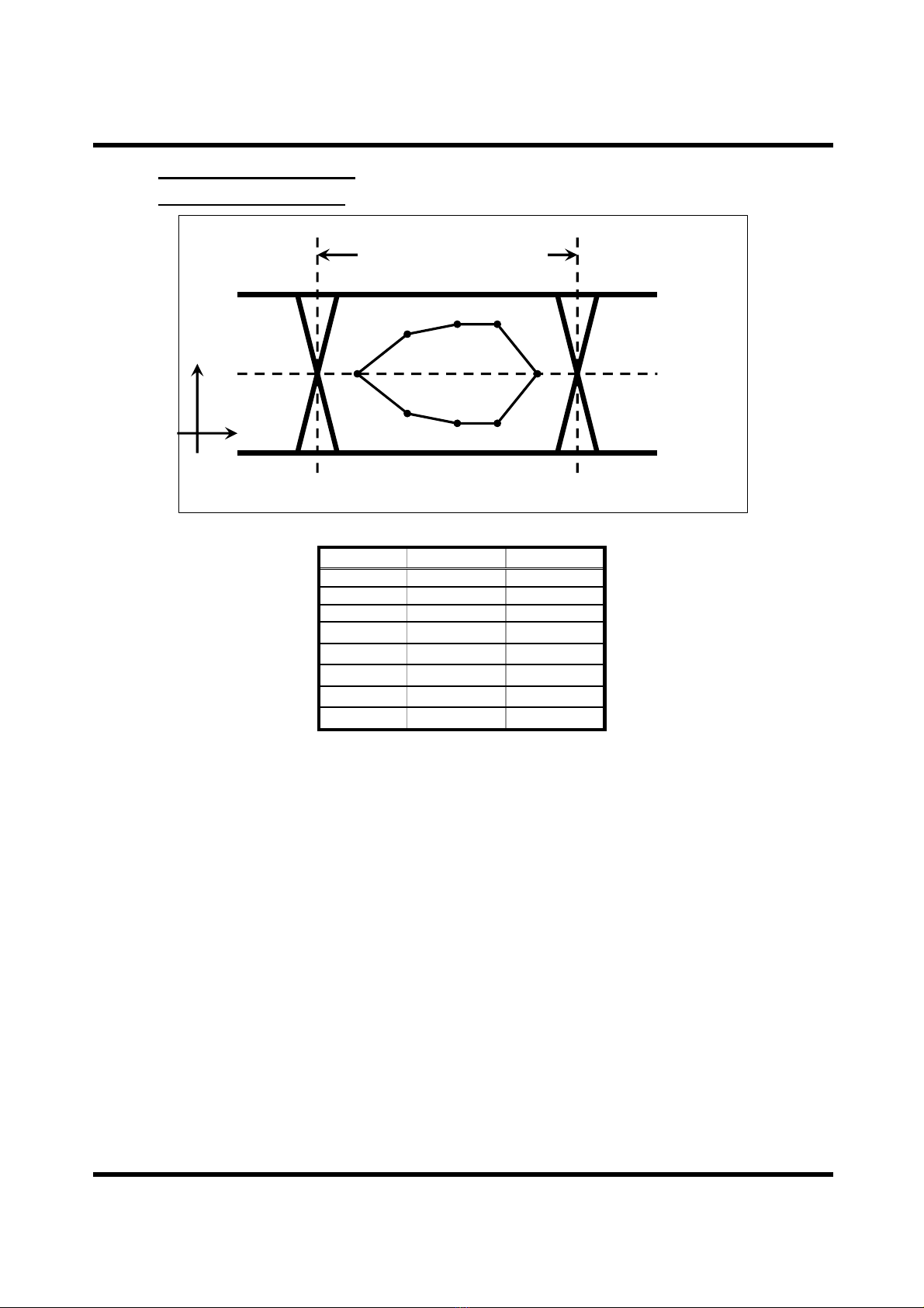
6. CML Line Eye diagrams
6.1. CML output Eye diagrams
Y=0mV
X=0 UI X=1 UI
1UI=1/(serial data rate)
Y
X
A
B C D
E
H G F
X[UI] Y[mV]
A 0.15 0
B 0.355 140
C 0.5 175
D 0.645 175
E 0.85 0
F 0.645 -175
G 0.5 -175
H 0.355 -140
THCS251_Rev.3.01_E
Copyright©2023 THine Electronics, Inc. THine Electronics, Inc.
20/33
SC: E
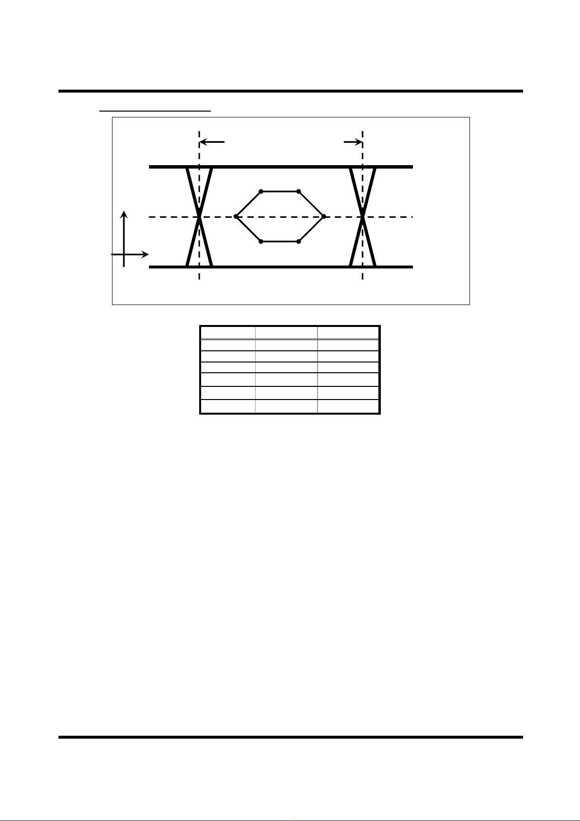
6.2. CML input Eye diagrams
Y=0mV
X=0 UI X=1 UI
1UI=1/(serial data rate)
Y
X
A
B C
D
F E
X[UI] Y[mV]
A 0.25 0
B 0.3 50
C 0.7 50
D 0.75 0
E 0.7 -50
F 0.3 -50
Table of contents
Other THine Transceiver manuals


