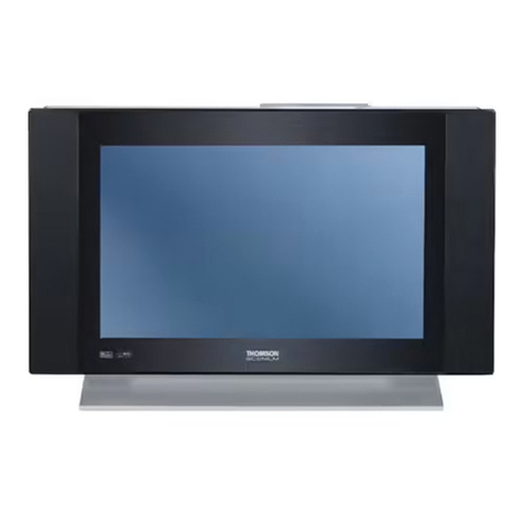
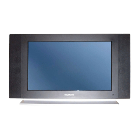
THOMSON RCA CR29TF420 Mounting instructions

CR29TF420
FEB/02
CR29TF420
Television
LatinAmericaAfterSales
Indianapolis, IN 46290 U.S.A.
SERVICE DATA INDEX
USE ISOLATION TRANSFORMER WHEN SERVICING
SAFETY NOTICE
Componentshaving specialsafety characteristicsare identifiedby a( ) onschematics andon theparts listin thisService Dataand itsbulletins.
Before servicing this instrument, it is important that the service technician read and follow the "Safety Precautions" in the Basic Service Data.
CR29TF420
Basic Service Data
FirstEdition-FirstPrinting
Copyright 2002 - Thomson multimedia Inc.
Printed in U.S.A. - Trademark(s)®Registered - Marca(s) Registrada(s)
Page
Number
Adjustments (Onscreen Display)................................................................................... 9
Circuit Decription........................................................................................................... 21
Disassembly ................................................................................................................... 5
IC Pin Descriptions ........................................................................................................ 15
Remote Control .............................................................................................................. 14
Replacement Partlist....................................................................................................... 37
Schematics
InterconnectDiagram.................................................................................................. 46
AV Switch .................................................................................................................. 47
Micro-Controller ........................................................................................................ 48
One Chip .................................................................................................................... 49
Power Supply............................................................................................................. 50
Stereo Decoder and Audio Output ............................................................................. 51
Tuner .......................................................................................................................... 52
Vertical and Horizontal Output.................................................................................. 53
Video Output.............................................................................................................. 54
ServicingandSafetyChecks ........................................................................................... 2
Specifications..................................................................................................................3
Troubleshooting Guides ................................................................................................. 24
Waveforms...................................................................................................................... 32
CAUTION: Modification or repair of this unit by unauthorized persons is a direct violation of FCC Rules Part 68.216 and could
result in risk of electric shock. You are urged to contact a qualified factory authorized service facility for repairs.
A-PDF MERGER DEMO

9
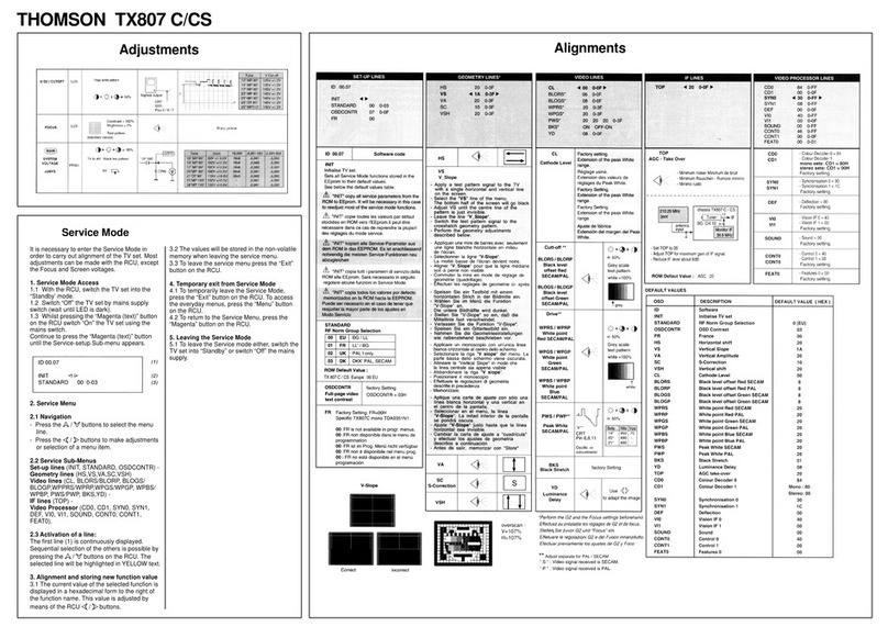
3. ON-SCREEN DISPLAY ADJUSTMENT
3.1 Memory Initialization (First Power On)
Before turn-on the set for the first time, it’s necessary to make a memory initialization of the Memory
Chip (IC102).
This adjustment is required only for the first power-on or wherever the Memory Chip have been
changed.
With the TV set unplugged from the AC Power keep pushed simultaneously the buttons “Channel
up” and “Channel down” in the front panel. Then plug it and wait 20 seconds before release the
buttons. Press “POWER”.
To certify that the initialization was success executed, it will appear the following message:
ILLUSTRATION 1
3.2 OSD Adjustment – Service Mode
To obtain the “SERVICE MENU” do the following procedure:
With the TV set unplugged from the AC Power keep pushed the button “Volume up” in the front
panel and plug it;
After 20 seconds release “Volume up” and press “Power”;
Press “Volume up” and “Volume down” simultaneously and will be displayed the “SERVICE
MENU”;
TO RUN AUTOMATIC
TUNING NOW
PLUG THE ANTENNA
<NO >YES
HS 1C VSH 21 SL 08
EW 1D WR 20 ADJ 0
PW 12 WG 20 A1 01
CP 15 WB 20 A2 02
TC 1D AGC 10 TC 03
VS 29 CD 03 OM 0
VA 05 SBL 0
SC 08 VSD 0
I2C 00 NORMAL

10
Press buttons “Channel up” and Channel down” to select the adjust to be done (hilighted in RED);
Press buttons “Volume up” and “Volume down” to do the adjust;
To cancel the “SERVICE MENU” unplug the set from the AC Power.
3.3 Service Menu Items
HS = HORIZONTAL SHIFT AGC = AGC ADJUST
EW = HORIZONTAL WIDTH CD = CATODE DRIVE LEVEL
PW = PIN CUSHION (CENTER) SBL = SERVICE BLANKING
CP = PIN CUSHION (EDGES) VSD = VERTICAL SERVICE SWITCH
TC = TRAPEZIUM CORRECTION SL = AUDIO LEVEL ADJUST
VS = VERTICAL SLOPE ADJ = STEREO ADJUST
VA = VERTICAL AMPLITUDE A1 = WIDEBAND
SC = VERTICAL LINEARITY A2 = SPECTRAL
I2C = STATUS OF I2C TC = CURRENT ADJUST
VSH = VERTICAL SHIFT OM = FACTORY PICTURE SETTINGS
WR/WG/WB = WHITE POINT ADJUST
3.4 AGC Adjustment
Apply a color bar pattern (RF Input) with 500µV signal;
Connect a DC Voltmeter, in the AGC pin of the tuner;
Adjust AGC to Zero and measure the voltage (V1);
Adjust AGC so that the indication on the voltmeter be (V1) - 1 ± 0.2V.
3.5 Stereo Adjustment
For the adjustments, proceed according to illustration 2;
Adjust output indicated by “A” to tension equal to half of VCC plus 1V ;
Adjust TC to an indication in the microAmpère meter of 24µA in the pin 17 of IC450;
Apply 300Hz/Mono/25KHz of deviation, 250mVrms, in the pin 29 of IC450;
Adjust SL to 500±20mVrms in the pins 15 and 38 of IC450;
Apply in the channel L=300Hz and in the channel R= 3k, 14% of generator Stereo modulation
DBX-NR (EIDEN BTSC );
Change ADJ from 0to 1. Check A1 and A2 after 1 second (if they varied);
After 1 second returns ADJ to 0. The stereo circuit will align automatically.

11
ILLUSTRATION 2
3.6 Vertical Adjustment
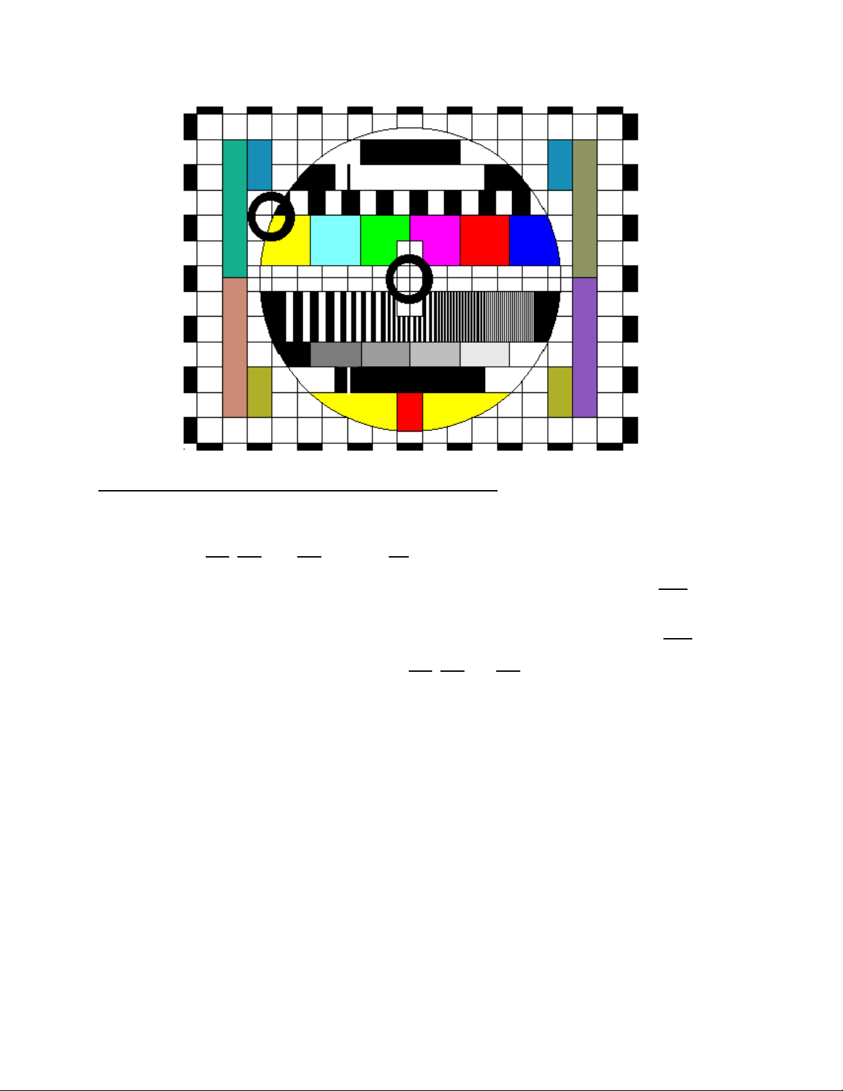
Apply a circle Pattern Philips signal (RF Input);
Using the remote control, set the MAGIC mode “ORIGINAL”;
Activate the adjustment mode display (SBL item). Adjust SBL from 0to 1. Blanking the bottom of
the screen;
Adjust VSH until the bottom of the pattern be aligned with the reference marks of the mechanical
center on picture tube (the central vertical line in the center of the tube);
Adjust VS until the central line be aligned with the half bottom of the screen (the central line of the
circle pattern in the half cut of the screen);
Return SBL from 1to 0value . The image could be compressed or expanded;
Select VA item and set its value to adjust the size of the picture (proportional height and width
picture);
If necessary readjust SC item and set its value to adjust the Linearity (acts in the top of the image)
and VA.
NOTE: The SC and VA adjustments are interdependent (they should be used together).
When the image to be decentralized in the vertical, to retouch VSH and/or VS
3.7 Horizontal Adjustment
Apply a Circle Pattern Philips signal at the antenna terminal. Set Magic ORIGINAL;
In the SERVICE MENU adjust EW for horizontal widht and HS for symetrical horizontal position of
the image;

12
Adjust PW to aligne the Pin Cushion effect in the vertical lines in both sides of the screen;
Adjust TC (trapezium) to aligne the vertical lines in both sides of the screen;
Adjust CP to aligne the Pin Cushion effect vertical lines in the for edges of the screen.
3.8 “FOCUS” Adjustment
Apply a Circle Pattern Philips signal at the antenna terminal. Magic ORIGINAL;
Adjust Focus V potenciometer (vertical) for the better focus on the vertical lines in the center of the
screen;
Adjust Focus H potentiometer (horizontal) for the better focus on the horizontal lines inthe center of
the screen;
Check the focus on the areas indicated below and readjust Fovus V na H if necessary.

13
3.9 White Balance Adjustment and Screen Adjustment
3.5.1- This adjustment must be done 20 minutes after turning on the TV set. Ambient illumination
should be less than 20 Lux;
3.5.2- Adjust WR,WG, and WB to 20 and CD to 03;
3.5.3- Turn the Screen Grid Potentiometer fully counter clockwise;
3.5.4- Short circuit C803 to Ground (located in the CPT PCI) and change the register VSD FROM
0 TO 1 (for cutting Vertical;
Deflection) and turn the Screen potentiometer gradually clockwise and set it to the point where a
thin bright line begin to appear on CPT. Remove the short circuit of C803 and change VSD FROM
1 TO 0;
3.5.5- Check the White Balance and readjust WR,WG and WB if necessary.

6.0 - OPERATION DESCRIPTION- CP01LR02 TELEVISION SET CIRCUIT
Fig.1- Block diagram
Speaker
The block diagram in Fig.1 shows how the TV set circuit works divided into 9 basic circuits.
6.1 - POWER SUPPLY
IC901, IC902, IC903, T901, Q901 and surrounding components (9xx).
This is a switching mode power supply designed to operate in AC power source from 99 Volts to 242 Volts
and 50/60 Hertz.
The main device is the TDA16846 (controller for switching mode power supplies).
In stand-by mode , the micro-controller disables the IC904 (+9Vdc regulator) ,turning-off the tuner ,the stereo
decoder ,the AV switches and the TV signal processor circuit . In this condition ,the horizontal and vertical
deflections and audio output circuits are stopped with a low current consumption . Only the micro-controller
is active .
The power-on is activate by the micro-controller (pin45) though the remote control or the power switch in the
front panel ,that turns-on the +9V supply waking up the circuit .
The output voltages are controlled by the IC901 through the opto coupler feedback (IC902) and a reference
voltage given by IC903 .
The basic output voltages are:
1. +130 Volts for the horizontal circuit;
2. +18 Volts for audio output circuits;
3. +9 Volts for TV signal processor, stereo decoder and AV circuits;
4. +5 Volts for microprocessor and memory circuits.
There are 3 basic protection mode:
1. AC power source undervoltage: the power supply will turn-off when the AC source is less than 90 Volts;
2. Power consumption limit: when the power consumption exceed 20% of the normal value;
3. Overvoltage outputs shutdown: when the output voltages exceed 20% of the normal values.
6.2 - TV SIGNAL PROCESSOR
IC501 and surrounding components.
The main device is the TDA8843, that combines all the functions for a multi-system color TV application with
closed caption.
4.Tuner
5. AV
switches
1. Power Supply
2. TV signal
processor
6. Stereo
decoder
8.Video
output
9.Horizontal
and vertical
deflections
7.Audio
output
3. Micro controller
21

The highlights of this device are:
-I2C bus serial I/O;
-Multi-standard vision IF circuit (45.75 MHz) with PLL demodulator;
-PAL/NTSC color decoder with automatic search system;
-Integrated luminance and chrominance circuit;
-RGB control circuit;
-8V supply voltage;
-Horizontal and vertical geometry processing.
6.3 – MICRO-CONTROLLER
IC101, and surrounding components.
This is a 8bit micro-controller dedicated for TV applications (M37274MA). It controls all the circuits by two
I2C bus lines. Main features:
- 8MHz crystal oscillator for internal timing.
- internal memory: ROM 40Kbytes and RAM 768 bytes.
- closed caption decoder.
- 5V supply voltage.
- 32KHz crystal oscillator for clock functions.
- high performance OSD.
An external E2PROM (IC102) with 4 Kb is used to keep the setup and calibration configuration by I2C bus
(channels, volume, horizontal and vertical geometry, etc.).
Front panel buttons and IR decoders are also realized by IC101.
6.4 - TUNER
TU201, and surrounding components.
This is a standard Frequency Synthesizer Tuner (FST Tuner) which covers VHF and UHF channels,
including cable channels (frequency range from 55.25 MHz to 801.25 MHz).
This device is controlled by I2C bus. The IF output signal (45.75 MHz) is connected to the IC501 through a
SAW filter (MF201).
6.5 - AV SWITCHES
IC470 , IC480 and surrounding components.
The external audio and video signals (AV1, AV2, AV3) are selected by the Micro Controller using two output
signals ( pin47 av2 and pin48 av1, IC101). The video signals are selected using IC480 (LA7221), and the
audio signals are selected using the IC470 (4052).
The selected video signal is connected to the TV signal processor external video input (pin17) and the
selected audio signal is connected to the stereo decoder IC450 (pins 12 and 41).
6.6 - STEREO DECODER
IC450 and surrounding components.
The main device is TDA9855 (stereo / sap decoder with DBX noise reduction system).
Using I2C bus, the IC101 can identify a stereo and SAP signals.
This device combines stereo decoder and audio processor with automatic volume level control, special
effects, volume/balance controls, bass control and treble control.
Q450 and Q450R are buffers for the audio output jacks (JA450).
6.7 - AUDIO OUTPUT
IC401, SP401, SP401R and surrounding components.
The main device is TDA2616 (stereo amplifier). The output signal is a 5+5 Watts with a 8 ohms speakers.
The input signals come from the stereo decoder (IC450 pins6 and 47).
22

This circuit uses external mute system (Q410) to minimize speaker noise during turn on/off.
6.8 - VIDEO OUTPUT
Q810, Q811, Q812, Q820, Q821, Q822, Q830, Q831, Q832 and surrounding components.
The RGB signals from the signal processor (pins 19,20,21) ,are amplified to the CRT using a cascode
transistors configuration.
6.9 - HORIZONTAL AND VERTICAL DEFLECTIONS
IC601, T701, T702, Q701 and surrounding components.
Vertical deflection circuit uses a TDA8177F (IC601 - vertical deflection booster) and operates with around
24V and provides output current to drive the yoke. The input signals are vertical drive + / - from the TV signal
processor (pin46 and 47 of IC501).
Horizontal deflection circuit uses 15.7KHz signal (HOUT_pin40 IC501) to drive the fly back transformer
(T701) and provides the output current to drive horizontal deflection coil (yoke) and others CTR voltages
(HV, focus, screen and etc.).
The vertical deflection circuit has one protection mode (turn-off the power supply if a fault situation is
detected) and the horizontal deflection circuit has two protection modes:
-turn-off the power supply if a HV over voltage is detected (X-ray protection);
-turn-off the power supply if a horizontal drive transistor (Q701) overstress is detected.
23

5
2. DISASSEMBLY INSTRUCTIONS
RemovalofmechanicalpartsandP.C.Boards.
2.1 Back Cabinet (refer to figure 2.1)
> Remove the screws, which secure the back cabinet to the front cabinet.
> Remove the screws, which secure the rear A/V input and output connectors.
> Removethebackcabinet.
2.2 CRT PCB (refer to figure 2.2/2.3)
Caution:
Beforeremovingtheanodecap,dischargeelectricitybecauseitcontainsahighvoltage. Beforeattemptingtoremove
or repair any PCB, unplug the power cord from the AC source.
> Removetheanodecap.
> Disconnectthegroundconnector(CM801).
> RemovetheCRTPCB.
2.3 Main PCB (refer to figure 2.2/2.3)
> Disconnectthefollowingconnectors: CM901,CM902,CM701,CM601,CM401andCM402.
> Unlock the PCB from the cabinet (both sides of the board).
> RemovetheMainPCB.
2.4 CRT (refer to figure 2.4)
> Removethefour(4)screws.
> RemovetheCRT.
Note:
TheREMOVALOFTHEANODECAP-AfterturningthepowerOFF,theremightstillbeapotentialvoltagethatisvery
dangerous. Whenremovingthe ANODECAP,make suretodischarge the anode'scappotential voltage. Donotuse
pliers to loosen or tighten the anode cap terminal. This may cause damage to the spring.

6

7

8

15
5 – DESCRIPTION OF THE FUNCTIONS – THE INTEGRATED CIRCUIT´S PINS
5.1 – IC 501 (TDA8843)
SIGN PIN DESCRIPTION
SNDIF 1 AUDIO IF INPUT
AUDIOEXT 2 EXTERNAL AUDIO INPUT
NC 3 NOT CONNECTED
NC 4 NOT CONNECTED
PLLLF 5 FILTER OF IF DECOUPLING
IFVO 6 COMPOSITE VIDEO OUTPUT
SCL 7 SERIAL CLOCK OUTPUT
SDA1 8 SERIAL DATA INPUT/OUTPUT (I2C-BUS)
DECBG 9 THERMAL STABILITY OF THE HORIZONTAL
CHROMA 10 SVHS CHROME VIDEO INPUT
CVBS/Y 11 INPUT FROM Y TO S-VHS
VP1 12 SUPPLY VOLTAGE (+8V)
CVBSint 13 COMPOSITE VIDEO INPUT
GND 14 GROUND
AUDIOOUT 15 AUDIO OUTPUT
CALDOC 16 DECOUPLING
CVBSext 17 EXTERNAL VIDEO INPUT
BLKIN 18 INPUT OF BEAM CURRENT LIMIT
BOUT 19 BLUE OUTPUT
GOUT 20 GREEN OUTPUT
ROUT 21 RED OUTPUT
BCLIN 22 INPUT OF BEAM CURRENT LIMIT/VERTICAL PROTECTION
RIN 23 OSD RED INPUT
GIN 24 OSD GREEN INPUT
BIN 25 OSD BLUE INPUT
FBLANK 26 OSD BLANKING
LUMIN 27 Y INPUT
LUMOUT 28 Y OUTPUT
B-YOUT 29 B-Y OUTPUT
R-YOUT 30 R-Y OUTPUT
B-YIN 31 B-Y INPUT
R-YIN 32 R-Y INPUT
REFO 33 SUB CARRIER REFERENCE OUTPUT
XTAL1 34 NTSC CRYSTAL CONECTION
XTAL2 35 PAL-M/N CRYSTAL CONECTION
COLOURPLL 36 COLOUR FASE FILTER
Pp2 37 SUPPLY VOLTAGE (+8V)
CVBSOUT 38 VIDEO OUTPUT
DECDIG 39 DECOUPLING OF SUPPLY
HOUT 40 OUTPUT OF HORIZONTAL PULSE
SAND/HFLY 41 SAND CASTLE PULSE
PH2LF 42 HORIZONTAL PHASE FILTER
PH1LF 43 CONTROL LOOP, HORIZONTAL OSC. FILTER
GND2 44 GROUND
EW/AVL 45 PULSE OF EAST-WEST CORRECTION
VDRIVE 46 OUTPUT OF VERTICAL PULSE
VDRIVE 47 OUTPUT OF VERTICAL PULSE
IFIIN1 48 IF INPUT 1

16
IFIIN2 49 IF INPUT 2
EHTO 50 HI VOLTAGE PROTECTION
VSC 51 FILTER OF VERTICAL
LREF 52 REFERENCE CURRENT INPUT
DECagc 53 AGC DECOUPLING
AGCOUT 54 AGC VOLTAGE DELAY OUTPUT
AUDEEN 55 AUDIO DEENPHASIS
DECSDEM 56 AUDIO DECOUPLING
5.2 – IC 1401 (TDA9181)
SIGN PIN DESCRIPTION
Cin 1 INPUT OF CHROME SINAL
INPSEL 2 SWITCH OF INPUT SELECTION
Y/CVBS2 3 Y INPUT (2)
DGND 4 GROUND
VDD 5 SUPPLY VOLTAGE
VCC 6 SUPPLY VOLTAGE
SC 7 SAND CASTLE PULSE INPUT
FSCSEL 8 GROUND
FSC 9 IDENTIFICAÇÃO DE SUB PORTADORA
SYS2 10 INPUT OF SYSTEM IDENTIFICATION (2)
SYS1 11 INPUT OF SYSTEM IDENTIFICATION (1)
Y/CVBS1 12 Y INPUT (1)
AGND 13 GROUND
Y/CVBSout 14 Y OUTPUT
OUTSEL 15 NOT CONNECTED
Cout 16 CHROME OUTPUT
5.3 - IC 601 (TDA8351)
SIGN PIN DESCRIPTION
Idrive (neg) 1 NON-INVERTING INPUT
VCC 2 SUPPLY VOLTAGE (12V)
Vp 3 SUPPLY VOLTAGE (55V)
VCC 4 SUPPLY VOLTAGE (–12V)
OUT 5 OUTPUT
OSS 6 SINAL REFERENCE
Idrive (pos) 7 INVERTING INPUT
5.4 - IC 102 (ST24CO4CB1)
SIGN PIN DESCRIPTION
AO 1 GROUND
A1 2 GROUND
A2 3 GROUND
VSS 4 GROUND
DAS 5 SERIAL DATA
SCL 6 SERIAL CLOCK
TEST 7 GROUND
VDD 8 SUPPLY VOLTAGE

17
5.5 - IC 430 (TDA1519A)
SIGN PIN DESCRIPTION
NINV 1 NON-INVERTING INPUT
GND 2 GROUND
RR 3 NOT CONNECTED
OUT(1) 4 OUTPUT ( 1 )
GND 5 GROUND
OUT( 2 ) 6 OUTPUT ( 2 )
Vp 7 SUPPLY VOLTAGE
M/SS 8 MUTE INPUT
INV 9 INVERTING INPUT
5.6 - IC 401 (TDA2616)
SIGN PIN DESCRIPTION
NINV1 1 NON-INVERTING INPUT 1
MUTE 2 MUTE INPUT
1/2Vp/GND 3 VOLTAGE (1/2 Vp)
OUT(1) 4 OUTPUT ( 1 )
GND 5 GROUND
OUT(2) 6 OUTPUT ( 2 )
Vp 7 SUPPLY VOLTAGE
INV1,2 8 INVERTING INPUT 1,2
NINV2 9 NON-INVERTING INPUT 2
5.7 - IC 901 (TDA16846)
SIGN PIN DESCRIPTION
OTC 1 OFF TIME CIRCUIT
PCS 2 PRIMARY CURRENT SIMULATION
RZI 3 REGULATION AND ZERO CROSSING INPUT
SRC 4 SOFT-STAR AND REGULATION CAPACITOR
OCI 5 OPTO COUPLER INPUT
FC2 6 FAULT COMPARATOR 2 (GND)
SYN 7 SYNCHRONIZATION INPUT
NC 8 NOT CONNECTED
REF 9 REFERENCE VOLTAGE AND CURRENT
FC1 10 FAULT COMPARATOR 1 (GND)
PVC 11 PRIMARY VOLTAGE CHECK
GND 12 GROUND
OUT 13 OUTPUT ( PWM PULSE)
VCC 14 SUPPLY VOLTAGE
5.8 - IC 904/905 (BA09ST,BA05ST)
SIGN PIN DESCRIPTION
CTL 1 ON/OFF CONTROL
VCC 2 INPUT VOLTAGE
GND 3 GROUND
OUT 4 REGULATED OUTPUT VOLTAGE
NC 5 NOT CONNECTED

18
5.9 - IC 1504 (LA7016)
SIGN PIN DESCRIPTION
VCC 1 SUPPLY VOLTAGE
IN2 2 EXTERNAL AUDIO INPUT
CTL 3 SWITCHING OF INPUTS CONTROL
OUT 4 AUDIO OUTPUT
GND 5 GROUND
NC1 6 NOT CONNECTED
IN1 7 NOT CONNECTED
NC2 8 TUNER AUDIO INPUT
5.10 - IC 450 (TDA9855)
SIGN PIN DESCRIPTION
TL 1 TREBLE CONTROL CAPACITOR, LEFT CHANNEL
B1L 2 BASS CONTROL CAPACITOR, LEFT CHANNEL
B2L 3 BASS CONTROL CAPACITOR, LEFT CHANNEL
OUTS 4 OUTPUT SUBWOOFER OR OUTPUT SURROUND SOUND
NC 5 NOT CONNECTED
OUTL 6 OUTPUT, LEFT CHANNEL
LOL 7 INPUT LOUDNESS, LEFT CHANNEL
CAV 10 AUTOMATIC VOLUME CONTROL CAPACITOR
VREF 11 REFERENCE VOLTAGE 0.5 VCC
LIL 12 INPUT LINE, LEFT CHANNEL
FIL 13 INPUT AUTOMATIC VOLUME CONTROL, LEFT CHANNEL
SOL 14 OUTPUT SELECTOR, LEFT CHANNEL
LOL 15 OUTPUT LINE CONTROL, LEFT CHANNEL
TW 16 CAPACITOR TIMING WIDEBAND FOR DBX
TS 17 CAPACITOR TIMING SPECTRAL FOR DBX
CW 18 CAPACITOR WIDEBAND FOR DBX
CS 19 CAPACITOR SPECTRAL FOR DBX
VEO 20 VARIABLE EMPHASIS OUTPUT FOR DBX
VEI 21 VARIABLE EMPHASIS INPUT FOR DBX
CNR 22 CAPACITOR NOISE REDUCTION FOR DBX
CM 23 CAPACITOR MUTE FOR SAP
CDEC 24 CAPACITOR DC-DECOUPLING FOR SAP
GND 25 GROUND
SDA1 26 SERIAL DATA INPUT/OUTPUT (I2C-BUS)
SCL 27 SERIAL CLOCK INPUT (I2C-BUS)
VCC 28 SUPPLY VOLTAGE
COMP 29 COMPOSITE INPUT SIGNAL
VCAP 30 CAPACITOR FOR ELECTRONIC FILTERING OF SUPPLY
CP1 31 CAPACITOR FOR PILOT DETECTOR
CP2 32 CAPACITOR FOR PILOT DETECTOR
CPH 33 CAPACITOR FOR PHASE DETECTOR
CADJ 34 CAPACITOR FOR PILTER ADJUSTMENT
CER 35 CERAMIC RESONATOR ( 503KHz)
CMO 36 CAPACITOR DC-DECOUPLING MONO
CSS 37 CAPACITOR DC-DECOUPLING STEREO/SAP
LOR 38 OUTPUT LINE CONTROL, RIGHT CHANNEL
SOR 39 OUTPUT SELECTOR, RIGHT CHANNEL
AVR 40 INPUT AUTOMATIC VOLUME CONTROL, RIGHT CHANNEL

19
LIR 41 INPUT LINE CONTROL, RIGHT CHANNEL
CPS2 42 CAPACITOR 2 PSEUDO FUNCTION
CPS1 43 CAPACITOR 1 PSEUDO FUNCTION
EOR 44 OUTPUT EFFECTS, RIGHT CHANNEL
VIR 45 INPUT VOLUME CONTROL, RIGHT CHANNEL
LDR 46 INPUT LOUDNESS, RIGHT CHANNEL
OUTR 47 OUTPUT, RIGHT CHANNEL
NC 48 NOT CONNECTED
SW 49 FILTER CAPACITOR FOR SUBWOOFER
B2R 50 BASS CONTROL CAPACITOR, RIGHT CHANNEL
B1R 51 BASS CONTROL CAPACITOR, RIGHT CHANNEL
TR 52 TREBLE CONTROL CAPACITOR
5.11 - IC 101 (M37274MA086SP) / (M37274MA-207SP)
SIGN PIN DESCRIPTION
HSYNC 1 PULSE INPUT OF HORIZONTAL SYNCHRONISM
VSYNC 2 PULSE INPUT OF VERTICAL SYNCHRONISM
MENU 3 ACCESS TO THE MENU BY THE FRONT PANEL
TV/AV 4 ACCESS TO THE TV/AV BY THE FRONT PANEL
VOL- 5 ACCESS TO THE VOL- BY THE FRONT PANEL
VOL+ 6 ACCESS TO THE VOL+ BY THE FRONT PANEL
PAL-N/PIP-ID 7 NOT CONNECTED
PROT 8 HI VOLTAGE PROTECTION
LIVRE2 9 NOT CONNECTED / PEAKING-SW (M37274MA-207SP)
SVHADET 10 CONECTION ID IN THE S-VHS INPUT
CH- 11 ACCESS TO THE CH- BY THE FRONT PANEL
CH+ 12 ACCESS TO THE CH+ BY THE FRONT PANEL
POWER 13 ACCESS TO THE POWER BY THE FRONT PANEL
IR 14 IR INPUT
PWR FAIL 15 POWER FAIL
NC1 16 NOT CONNECTED
NC2 17 NOT CONNECTED
AVCC 18 SUPPLY VOLTAGE
HLF 19 CCD OSCILLATOR
RVCO 20 CCD POSITION
VHOLD 21 CCD VERTICAL FREQUENCY
CVIN 22 COMPOSITE VIDEO INPUT
CNVSS 23 GROUND
XIN 24 OSCILLATOR (8MHz)
XOUT 25 OSCILLATOR (8MHz)
VSS 26 GROUND
VCC 27 SUPPLY VOLTAGE
XCIN 28 OSCILLATOR (32KHz)
XCOUT 29 OSCILLATOR (32KHz)
RESET 30 INPUT OF RESET VOLTAGE
PAL-M 31 SWITCH VOLTAGE OUTPUT OF PAL-M SYSTEM
PAL-N 32 SWITCH VOLTAGE OUTPUT OF PAL-N SYSTEM
SW-CURVAS 33 NOT CONNECTED
CLT 34 REFERENCE TO THE INPUT SELECTION OF COMB FILTER
SYS1 35 COLOUR SYSTEM ID
SDA2 36 SERIAL DATA ( 2 )

20
SDA1 37 SERIAL DATA ( 1 )
SCL2 38 SERIAL CLOCK ( 2 )
SCL1 39 SERIAL CLOCK ( 1 )
SOMBRA 40 SHADOW IN THE SCREEN TO CONTRAST CHARACTERS
GAME 41 GAME AUDIO OUTPUT
PROD 42 TEST POINT
SYS2 43 COLOUR SYSTEM ID
DESMAG 44 TENSÃO TEMPORIZADA P/ ACIONAMENTO DA DESMAG. AUT.
POWER 45 TENSÃO PARA CHAVEAMENTO DE LIGA / DESLIGA
MUTE 46 AUDIO MUTE
AV2 47 A/V INPUT SWITCH
AV1 48 A/V INPUT SWITCH
BLK 49 BLANKING OUTPUT OF CHARACTER GENERATOR
B 50 BLUE OUTPUT OF CHARACTER GENERATOR
G 51 GREEN OUTPUT OF CHARACTER GENERATOR
R 52 RED OUTPUT OF CHARACTER GENERATOR

14
4 – REMOTE CONTROL
Model CR29TF420
NOTE:Consult the original r. c.manufacturerdocumentationto access the schematic
diagramandthereplacementpartslist.
The “MENU” button contains the following operations:
Other THOMSON TV manuals

THOMSON
THOMSON 42M61NF21 User manual

THOMSON
THOMSON TX92F User manual

THOMSON
THOMSON 14MS73F User manual

THOMSON
THOMSON ZPN054102 User manual

THOMSON
THOMSON 28VT68N User manual

THOMSON
THOMSON 21DG15CH User manual

THOMSON
THOMSON easytv 24HD2S13 User manual

THOMSON
THOMSON ETC210 User manual

THOMSON
THOMSON ETC310 User manual

THOMSON
THOMSON IFC230 User manual

THOMSON
THOMSON CR14300 Installation guide

THOMSON
THOMSON DTH 8550 - User manual

THOMSON
THOMSON 20DG76C User manual

THOMSON
THOMSON ICC20 User manual

THOMSON
THOMSON 24WK23U User manual

THOMSON
THOMSON 72MK89D User manual

THOMSON
THOMSON 21DU21C User manual

THOMSON
THOMSON DTI6300 User manual

THOMSON
THOMSON G27693 Instruction Manual

THOMSON
THOMSON 25DG16ET User manual