Topward 8112 User manual

INSTRUCTION
MANUAL
DIGITAL
FUNCTION
GENERATOR
MODEL:
8112
if.
To
pwa
rd
TABLE
of
CONTENTS
Picture
of
Model
8112
.....................................
Introduction..................................................
Before
we
Begin..........Q....................................
Front
Panel
of
the
Model
8112
.......................w.....
Front
Panel
Description.......................................
Operating
Instructions........................................
8
Operating
Cautions............................................1D
Theory
of
Operation...........................................11
Calibration...................................................1a
Troubleshooting...............................................16
Adjustfient
Location...........................................20
Block
Diagram.................................................21
Circuit
Diagram...............................................22
Component
Layout..............................................26
Specifications................................................2?
U'TJ-‘bJN‘
part5
List-cotton...onto..-ole-InInca-Ilse.-liooooooco-ogunooozg
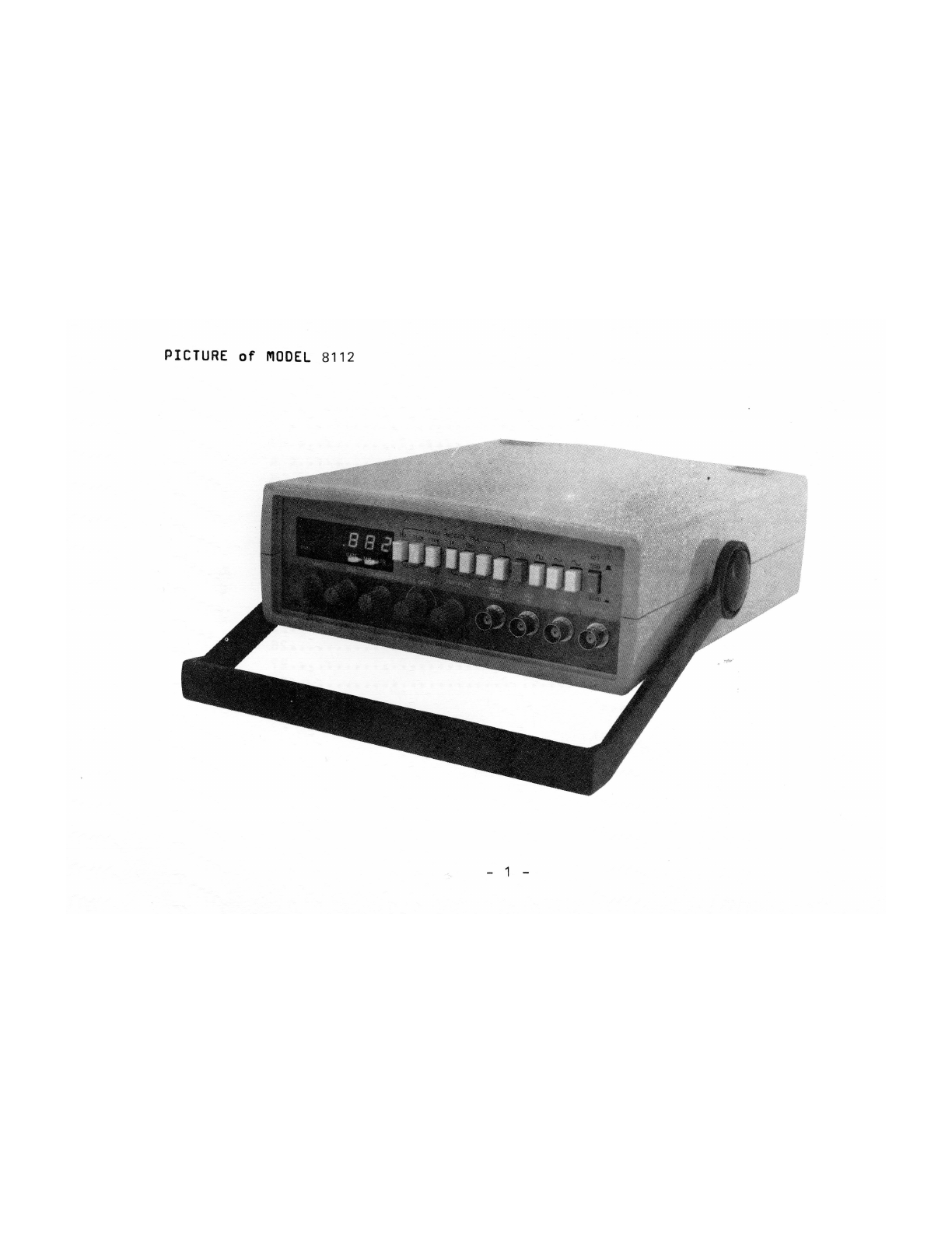
PICTURE
of
MODEL
8112
x‘
\\
\
\R
>
INTRODUCTION
The
Topward
8112
is
a
portable,
bench
type
multi-purpose
digital
function
generator/counter
capable
of
producing
5
different
waveforms.
These
are
Sine,
Square,
Triangle,
Pulse
and
Ramp.
The
model
8112
features:
Adjustable
frequency
range
from
0.1
Hz
to
2
MHz
in
7
ranges,
variable
output
amplitude
from
5
mV
to
20
Vp-p,
variable
symmetry/duty
cycle
from
5%
to
95%
in
the
Ramp/Pulse
mode,
continuous
or
externally
controlled
outputs,
DC
offset
between
—10
V
to
+10
U
can
be
added
to
all
output
waveforms,
inverted
and
attenuated
output,
built-in
100
MHz
frequency
counter
with
25
mV
input
sensitivity.
-
2 _
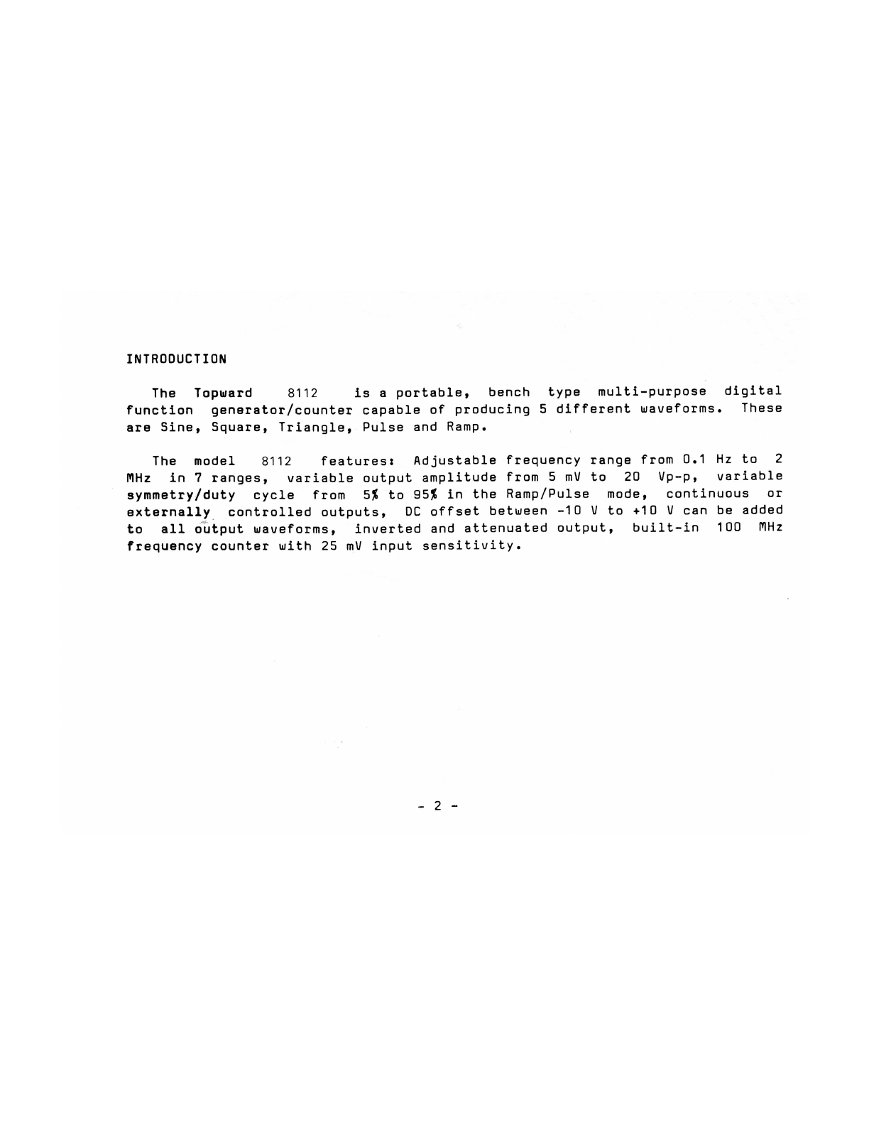
FRONT
PANEL
of
the
MODEL
8112
Figure
—
1
12
11
T
9
FREQUENCY
RANGE
Hz/GATE
THME
ATT
1M
TOOK
10K
1K
100
10
EU__N_C
m
N
%
OdB..I.
‘
__
LIEII+IEI_
I+RLIIfl
I
[TIMI]
JET”
OVFL
GATE
KHz
Hz
QJOTS
0
IS
108
COUNT.
~30dB
.-.
fl.
PULL
TO
VAR
AMPLITUDE
SYNC
VICF
COUNT.
OUTPUT
MAIN
FINE
.
RAMP/PULSE
DC
OFFSET
POWER
OUT
IN
PULL
TO
INVERT
"
‘‘‘‘‘
.C‘P
Q“
I
l!
Topward
DIGITAL
FUNCTION
GENERATOR
81
12
+
[NW
@®@@
h
13
1O
FRONT
PANEL
DESCRIPTION
The
following
is
an
explanation
of
the
function
of
the
front
panel
controls
and
connectors.
Please
refer
to
Figure
1
for
location
of
each
control/connector.
1.
POWER/AMPLITUDE
“
This
is
the
main
power
switch
and
the
amplitude
adjustment
knob.
Turning
the
control
clockwise
will
increase
the
amplitude.
2.
FUNCTION
-
This
bank
of
switches
is
used
to
select
the
output
waveform.
Only
one
of
these
switches
can
be
depressed
at
a
time.
3.
FREQUENCY
CONTROL
_
This
pair
of
knobs
is
used
to
adjust
the
output
frequency.
The
frequency
is
dependent
upon
the
setting
of
this
pair
of
knobs
and
the
RANGE/GATE
TIME
switches
(4).
Pulling
out
the
FINE
control
knob
(3)
will
invert
the
pulse
output.
a.
RANGE/GATE
TIME
-
This
bank
of
switches
is
used
to
select
the
frequency
range
produced.
At
the
same
time,
the
counter
gate
time
is
changed.
5.
RAMP/PULSE
-
This
knob
is
used
to
adjust
the
duty
cycle
of
the
Square
or
Triangle
waveforms.
when
the
knob
is
turned
to
CAL.
(fully
CCN
position),
the
duty
cycle
is
fixed
at
50%.
Otherwise,
the
duty
cycle
is
adjustable
between
5
to
95%.
_
5
-
FRONT
PANEL
DESCRIPTION
The
following
is
an
explanation
of
the
function
of
the
front
panel
controls
and
connectors.
lease
refer
to
Figure
1
for
location
of
each
control/connector.
1.
POWER/AMPLITUDE
n
This
is
the
main
power
switch
and
the
amplitude
adjustment
knob.
Turning
the
control
clockwise
will
increase
the
amplitude.
2.
FUNCTION
—
This
bank
of
switches
is
used
to
select
the
output
waveform.
Only
one
of
these
switches
can
be
depressed
at
a
time.
3.
FREQUENCY
CONTROL
—
This
pair
of
knobs
is
used
to
adjust
the
output
frequency.
The
frequency
is
dependent
upon
the
setting
of
this
pair
of
knobs
and
the
RANGE/GATE
TIME
switches
(4).
Pulling
out the
FINE
control
knob
(3)
will
invert
the
pulse
output.
a.
RANGE/GATE
TIME
-
This
bank
of
switches
is
used
to
select
the
frequency
range
produced.
At
the
same
time,
the
counter
gate
time
is
changed.
5.
RAMP/PULSE
-
This
knob
is
used
to
adjust
the
duty
cycle
of
the
Square
or
Triangle
waveforms.
when
the
knob
is
turned
to
EAL.
(fully
new
position),
the
duty
cycle
is
fixed
at
50%.
Otherwise,
the
duty
cycle
is
adjustable
between
5
to
95$.
_
5
-
B.
ATTENUATOR
—
when
this
push
button
is
out,
the
output/input
signal
is
unchanged.
If
the
switch
is
depressed,
the
Output/Input
signal
is
reduced
by
30
dB
(Generator
output
/
Counter
input).
7.
DC
OFFSET
-
This
knob
allows
a
variable
DC
voltage
between
~1O
V
to
+10
V
to
be
added
to
the
output
signal.
Note
that
the
knob
has
to
be
pulled
out
for
the
offset
to
affect
the
signal.
When
the
control
is
pushed
in,
no
offset
voltage
is
added.
8.
OUTPUT
—
This
connector
provides
the
output
signal
for
all
waveforms.
9.
FUNC/CDUNT
-
When
the
switch
is
out,
the
8
digits
DISPLAY
(11)
shows
the
generator
frequency.
When
the
switch
is
in,
the
DISPLAY
(11)
shows
the
input
frequency
of
counter.
10.
COUNTER
IN
-
This
is
the
input
connector
for
the
1OOMH2
frequency
counter.
FUNC/COUNT
switch
(9)
must
be
depressed.
11.
FREQUENCY
DISPLAY
-
This
is
a 6
digits
LED
display
that
shows
the
output
frequency
of
the
main
generator
or
the
input
frequency
of
the
counter.
12.
INDICATORS
-
OVFL,
GATE,
KHz,
Hz
LEDs
enunciate
frequency
overflow,
gate
time
and
frequency
units
in
KHz,
Hz.
-
5
_
B.
ATTENUATDR
—
When
this
push
button
is
out,
the
output/input
signal
is
unchanged.
If
the
switch
is
depressed,
the
Output/Input
signal
is
reduced
by
30
dB
(Generator
output
/
Counter
input).
7.
DC
OFFSET
-
This
knob
allows
a
variable
DC
voltage
between
~10
V
to
+10
V
to
be
added
to
the
output
signal.
Note
that
the
knob
has
to
be
pulled
out
for
the
offset
to
affect
the
signal.
When
the
control
is
pushed
in,
no
offset
voltage
is
added.
8.
DUTPUT
-
This
connector
provides
the
output
signal
for
all
waveforms.
9.
FUNC/CDUNT
—
When
the
switch
is
out,
the
5
digits
DISPLAY
(11)
shows
the
generator
frequency.
When
the
switch
is
in,
the
DISPLAY
(11)
shows
the
input
frequency
of
counter.
10.
COUNTER
IN
-
This
is
the
input
connector
for
the
1DDNH2
frequency
counter.
FUNC/CDUNT
switch
(9)
must
be
depressed.
11.
FREQUENCY
DISPLAY
-
This
is
a
6
digits
LED
display
that
shows
the
output
frequency
of
the
main
generator
or
the
input
frequency
of
the
counter.
12.
INDICATORS
—
DVFL,
GATE,
KHz,
Hz
LEDs
enunciate
frequency
overflow,
gate
time
and
frequency
units
in
KHz,
Hz.

13.
VCF
IN
-
This
input
is
used
to
modulate
the
main
frequency
to
1000:1
with
an
external
source
of
0
—
SVDC.
14.
SYNC
OUT
-
This
connector
supplies
a
TTL
compatible
output
signal
which
is
unaffected
by
either
the
FUNCTION
(2)
or
AMPLITUDE
(1)
controls.
The
output
frequency
is
the
same
as
that
of
OUTPUT
signal
(8).
13.
VCF
IN
-
This
input
is
used
to
modulate
the
main
frequency
to
1ODD:1
with
an
external
source
of
0
—
SVDC.
14.
SYNC
OUT
-
This
connector
supplies
a
TTL
compatible
output
signal
which
is
unaffected
by
either
the
FUNCTION
(2)
or
AMPLITUDE
(1)
controls.
The
output
frequency
is
the
same
as
that
of
OUTPUT
signal
(8).
_
7
-
OPERATING
INSTRUCTIONS
1.
2.
Instrument
Turn-on
UARNING:
Before
applying
power
to
your
8112
,
make
sure
that
the
input
voltage
is
set
to
your
power
source.
A.
Connect
the
8112
to
an
AC
power
source
and
turn
on
the
POWER
switch
(1).
Main
Generator
A.
Select
the
desired
waveform
using
the
FUNCTION
switch
(2).
To
generate
a
ramp
or
pulse
output,
turn
on
the
RAMP/PULSE
knob
(5)
and
set
the
desired
duty
cycle.
B.
Set
the
desired
Frequency
with
the
FREQUENCY
control
(3)
and
the
RANGE
switches
(4).
C.
Adjust
the
output
amplitude
with
the
AMPLITUDE
control
(1)
to
the
desired
level.
If
a
very
small
signal
is
required,
depress
the
ATTENUATDR
switch
(6).
D.
Set
DC
Offset
voltage
with
the
DC
OFFSET
control
(7).
E.
Use
the
SYNC
output
terminal
(14)
if
TTL
compatible
level
is
required.
OPERATING
INSTRUCTIONS
1.
2.
Instrument
Turn—on
WARNING:
Before
applying
power
to
your
8112
,
make
sure
that
the
input
voltage
is
set
to
your
power
source.
A.
Connect
the
8112
to
an
AC
power
source
and
turn
on
the
POWER
switch
(1)-
Main
Generator
A.
Select
the
desired
waveform
using
the
FUNCTION
switch
(2).
To
generate
a
ramp
or
pulse
output,
turn
on
the
RAMP/PULSE
knob
(5)
and
set
the
desired
duty
cycle.
8.
Set
the
desired
frequency
with
the
FREQUENCY
control
(3)
and
the
RANGE
switches
(4).
C.
Adjust
the
output
amplitude
with
the
AMPLITUDE
control
(1)
to
the
desired
level.
If
a
very
small
signal
is
required,
depress
the
ATTENUATUR
Smitch
(B)
o
D.
Set
DC
Offset
voltage
with
the
DC
OFFSET
control
(7).
E.
Use
the
SYNC
output
terminal
(14)
if
TTL
compatible
level
is
required.

F.
Pull
out
the
INVERT
switch
(3)
to
introduce
a
180
degree
phase
shift.
Voltage
Controlled
Frequency
A.
Supply
a
trim
voltage
between
0
and
5
VDC
to
the
VCF
IN
terminal
(13).
The
main
frequency
will
be
varied
over
1DUU:1.
Frequency
Counter
A.
Push
in
the
FUND/COUNT
switch
(9).
8.
Apply
input
signal
to
COUNT
IN
(10).
C.
Select
GATE
TIME
(4)
for
best
resolution.
0.
Use
ATTANUATDR
(6)
for
large
input
signal
to
avoid
damage
instrument.
-
g
-
to
the
F.
Pull
out
the
INVERT
switch
(3)
to
introduce
a
180
degree
phase
shift.
Voltage
Controlled
Frequency
A.
Supply
a
trim
voltage
between
0
and
5
VDC
to
the
VCF
IN
terminal
(13).
The
main
frequency
will
be
varied
over
1000:1.
Frequency
Counter
A.
Push
in
the
FUND/COUNT
switch
(9).
3.
Apply
input
signal
to
COUNT
IN
(10).
C.
Select
GATE
TIME
(4)
for
best
resolution.
D.
Use
ATTANUATUR
(B)
for
large
input
signal
to
avoid
damage
to
the
instrument.
OPERATING
CAUTIDNS
To
assure
operation
within
the
published
specifications,
allow
the
unit
to
warm
up
and
stabilize
for
at
least
20
minutes.
Failure
to
observe
the
operating
procedure
listed
below
will
damage
to
the
unit
and
void
your
warranty.
Do
not
supply
more
than
10
Volts
(
AC
+
DC
)
into;
Output
terminal
(8)
VCF
IN
terminal
(13)
SYNC
terminal
(14)
_
10
-
result
in
TFB~8111
OPERATING
CAUTIDNS
To
assure
operation
within
the
published
specifications.
allow
the
unit
to
warm
up
and
stabilize
for
at
least
20
minutes.
Failure
to
observe
the
operating
procedure
listed
below
will
result
in
damage
to
the
unit
and
void
your
warranty.
TFG-8111
Do
not
supply
more
than
10
Volts
(
AC
+
DC
)
into:
Output
terminal
(8)
VCF
IN
terminal
(13)
SYNC
terminal
(1h)
_
10
_
THEORY
OF
OPERATION
Counter
Section
1.
Counter
Amplifier
(refer
to
circuit
diagram
sheet
1)
A.
The
buffer
amplifier
(03
and
04)
make
up
the
impedance
buffer
circuit.
B.
USA-U58
form
a
secondary
high
voltage
gain
stage.
05
and
05
form
a
level
shifter.
Counter
Control
Circuit
(refer
to
circuit
diagram
sheet
4)
A.
U14
(72160)
is
a
single
chip
counter
IC.
U13
and
CREE-ERAS
form
a
gate
time
selecting
circuit.
8.
CRaa—CRSA
form
a
decimal
point
selecting
circuit
and
H2,
KHz
indicating
circuit.
C.
U15A-U160
form
a
generator
frequency
display
/
counter
input
frequency
display
selecting
circuit.
D.
U1:
is
a
divide~by~ten
IC,
use
for
the
high
frequency
input
measurement.
Generator
Section
1.
Tuning
Amplifier,
Summing
Amplifier
and
Constant
Current
Source
(refer
to
circuit
diagram
sheet
2)
_
11
_
A.
The
tuning
amplifier
is
a
non-inverting
input
amplifier
(UBA),
providing
a
fixed
voltage
for
frequency
control
MAIN
and
FINE
(3).
U88
is
a
voltage
buffer
IE,
buffering
the
variable
control
voltage
of
frequency
control
MAIN
and
FINE
(3).
B.
The
summing
amplifier
(U6
and
Q?)
sums
each
current
from
the
VCF
input
and
the
tuning
amplifier
output.
The
output
voltage
of
the
amplifier
is
a
weighted
average
of
the
input
signal
voltages.
The
frequency
control
MAIN
.
and
FINE
(3)
varies
the
amount
of
voltage
which
determines
the
generator
output
frequency.
C.
U?
and
Q8
generate
equalizing
positive
and
negative
voltages
for
the
current
source
circuit.
The
current
source
circuit
includes
positive
current
source
(U9
and
09)
and
negative
current
source
(U10
and
Q10).
The
positive
and
negative
current
values
are
determined
by
frequency
control
MAIN
and
FINE
(3).
Triangle
Generator
and
Comparator
(refer
to
circuit
diagram
sheet
2)
The
triangle
waveform
from
the
triangle
generator
is
apply
to
the
voltage
comparator
which
acts
as
an
amplitude
limiter.
As
the
triangle
waveform
alternately
crosses
the
upper
and
lower
switching
levels
(refer
to
R47-R50)
of
the
limiter
input,
a
square
wave
is
generated
at
the
output
of
the
voltage
comparator
(U11).
The
square
is
feedback
to
the
triangle
generator
where
it
controls
the
charge
/
discharge
cycle
of
the
triangle
output.
-
12
-
A.
The
tuning
amplifier
is
a
non-inverting
input
amplifier
(UBA),
providing
a
fixed
voltage
for
frequency
control
MAIN
and
FINE
(3).
USE
is
a
voltage
buffer
IE,
buffering
the
variable
control
voltage
of
frequency
control
MAIN
and
FINE
(3).
B.
The
summing
amplifier
(U6
and
a?)
sums
each
current
from
the
VCF
input
and
the
tuning
amplifier
output.
The
output
voltage
of
the
amplifier
is
a
weighted
average
of
the
input
signal
voltages.
The
frequency
control
MAIN
,
and
FINE
(3)
varies
the
amount
of
voltage
which
determines
the
generator
output
frequency.
E.
U7
and
Q8
generate
equalizing
positive
and
negative
voltages
for
the
current
source
circuit.
The
current
source
circuit
includes
positive
current
source
(U9
and
D9)
and
negative
current
source
(U10
and
010).
The
positive
and
negative
current
values
are
determined
by
frequency
control
MAIN
and
FINE
(3).
Triangle
Generator
and
Comparator
(refer
to
circuit
diagram
sheet
2)
The
triangle
waveform
from
the
triangle
generator
is
apply
to
the
voltage
comparator
which
acts
as
an
amplitude
limiter.
As
the
triangle
waveform
alternately
crosses
the
upper
and
lower
switching
levels
(refer
to
R47—R50)
of
the
limiter
input,
a
square
wave
is
generated
at
the
output
of
the
voltage
comparator
(U11).
The
square
is
feedback
to
the
triangle
generator
where
it
controls
the
charge
/
discharge
cycle
of
the
triangle
output.
_
12
-

3.
Sine
Shaper
and
PRE-Amplifier
(refer
to
circuit
diagram
sheet
3)
A.
'To
obtain
a
sine
wave.
The
triangle
wave
is
shaped
by
a
diode
network
(CR16
-
CR31),
in
the
sine
snapper.
There
are
four—stage
diodes
network
serves
as
a
non-linear
load
which
varies
the
attenuation
of
the
input
triangle
according
to
its
level.
B.
The
PRE-Amplifier
is
a
non-inverting
closed
loop
amplifier.
Q15
and
Q16
form
the
differential
input
stage
that
provides
DC
stability.
Q17
forms
the
second
gain
stage.
Q18
and
019
are
the
output
buffer
circuit.
4.
Output
Amplifier
(refer
to
circuit
diagram
sheet
3)
The
output
amplifier
works
the
same
manner
as
PRE-Amplifier,
and
provides
a
50
ohms
low
output
impedance
for
OUTPUT
terminal
(8).
-13-
3.
4.
Sins
Shaper
and
PRE-Amplifier
(refer
to
circuit
diagram
sheét
3)
A.
‘To
obtain
a
sine
wave.
The
triangle
wave
is
shaped
by
a
diode
network
(CR1B
-
CR31),
in
the
sine
shapper.
There
are
four—stage
diodes
network
serves
as
a
non-linear
load
which
varies
the
attenuation
of
the
input
triangle
according
to
its
level.
B.
The
DRE-Amplifier
is
a
non-inverting
closed
loop
amplifier.
Q15
and
Q15
form
the
differential
input
stage
that
provides
DC
stability.
017
forms
the
second
gain
stage.
018
and
019
are
the
output
buffer
circuit.
Output
Amplifier
(refer
to
circuit
diagram
sheet
3)
The
output
amplifier
works
the
same
manner
as
DRE-Amplifier,
and
provides
a
50
ohms
low
output
impedance
for
OUTPUT
terminal
(8).
_
13
-

CALIBRATION
CAUTIDNS:
Services
performed
by
unauthorized
person
will
void
your
warranty.
To
assure
the
most
stable
operation
possible,
your
Model
8112
should
be
periodically
adjusted.
To
perform
the
following
adjustment
procedures,
you
will
need
a
Phillips
screwdriver,
Timer/Counter,
Voltmeter,
an
Oscilloscope
(SDMHz
minimum),
Distortion
meter,
and
high
frequency
(up
to
1ODNH2)
signal
generator.
Calibration
be
performed
under
liboratory
conditions
having
an
ambient
temperature
of
18°
to
28°c(62°
to
82°F),
and
relative
humidity
of
less
then
80%.
As
you
perform
this
procedure,
please
refer
to
the
adjustment
location
drawing.
1.
Set
the
8112
controls
as
follows:
RANGE
(a)
............................
1K
FUNCTION
(2)
.........................
Av
DC
OFFSET
(7)
........................
OFF
AMPLITUDE
(1)
........................
cm
(Max.)
RAMP/PULSE
(s)
.......................
cum
(CAL)
FREQUENCY
NAIN
&
FINE
(3)
............
cw
(Max.)
2.
Connector
OUTPUT
(8)
on
Counter
1202
(or
equivalent),
adjust
R127
(ZNHz
ADJ)
to
display
2.3KH2
i
SUHz.
-
14
-
CALIBRATION
CAUTIUNS:
Services
performed
by
unauthorized
person
will
void
your
warranty.
To
assure
the
most
stable
operation
possible,
your
Model
8112
should
be
periodically
adjusted.
To
perform
the
following
adjustment
procedures,
you
will
need
a
Phillips
screwdriver,
Timer/Counter,
Voltmeter,
an
Oscilloscope
(SUMHz
minimum),
Distortion
meter,
and
high
frequency
(up
to
1DOMH2)
signal
generator.
Calibration
be
performed
under
liboratory
conditions
having
an
ambient
temperature
of
1a“
to
28“r(62“
to
82°F),
and
relative
humidity
of
less
then
80%.
As
you
perform
this
procedure,
please
refer
to
the
adjustment
locatidn
drawing.
1.
Set
the
8112
controls
as
follows:
RANGE
(a)
............................
1K
FUNCTION
(2)
.........................
AV
0:
OFFSET
(7)
........................
DFF
AMPLITUDE
(1)
........................
cw
(Max.)
RAMP/PULSE
(5)
.......................
cow
(CAL)
FREQUENCY
MAIN
&
FINE
(3)
............
cw
(Max.)
2.
Connector
OUTPUT
(8)
on
Counter
1202
(or
equivalent),
adjust
R127
(ZMHz
ADJ)
to
display
2.3KHZ
:
SUHZ.
-
14
-
3.
Select
RANGE(4)
to
1
K
and
FUNCTION
(2)
to
SINE.
Set
the
FREQUENCY
MAIN
&
FINE
(3)
to
read
1KHz
on
1202
.
Connect
the
OUTPUT
(8)
to
a
distortion
meter
TDA-71O
(or
equivalent).
Adjust
R13O
(SINE
DIST1),
R131
(SINE
DISTZ)
for
minimum
distortion.
4.
Select
FUNCTION
(2)
to
TRIANGLE.
Turn
the
AMPLITUDE
(1)
to
mid
location.
Connect
the
output
to
an
voltmeter.
Adjust
R135
(PA
DC)
to
be
DC
:
10mV.
Turn
the
AMPLITUDE
(1)
to
maximum
location.
Connect
the
OUTPUT
(8)
to
an
oscilloscope.
Adjust
R134
(TRI
ANPL)
to
let
the
Vp-p
of
triangle
wave
be
20.8V
1"
0.2V.
5.
Select
FUNCTION
(2)
to
SINE.
Adjust
R132
(SINE
DC)
to
let
DC
offset
be
DC
OV
i
10mV.
Adjust
R133
(SINE
AMPL)
to
let
the
Vp—p
of
sine
wave
be
20.8V
1
0.2V.
5.
Select
FUNCTION
(2)
to
SQUARE.
Adjust
R128
to
let
the
upper
level
of
square
wave
be
+10.4V
i
O.1V.
Adjust
R129
to
let
the
lower
level
of
square
wave
be
-10.4V
1
O.1V.
7.
Press
the
FUNC/COUNT
switch
(9)
in.
Connect
a
1OMHz
1
1PPM
standard
frequency
to
the
COUNTER
input
(10).
Adjust
trimmer
capacitor
C2
until
the
display
reads
000.000
KHZ
1
1
digits
(Hz).
(with
DVFL
LED
lit).
Set
the
RANGE
switch
(4)
to
1
MHz.
Apply
a
100MHz
SOmV
signal
to
COUNT
input
(10).
Adjust
trimmer
resistor
R126
to
let
the
display
be
stable.
_
15
_
3.
Select
RANGE(4)
to
1
K
and
FUNCTION
(2)
to
SINE.
Set
the
FREQUENCY
nAIu
&
FINE
(3)
to
read
1KHz
on
1202
.
Connect
the
OUTPUT
(8)
to
a
distortion
meter
TBA-710
(or
equivalent).
Adjust
R130
(SINE
DIST1).
R131
(SINE
DISTZ)
for
minimum
distortion.
h.
Select
FUNCTION
(2)
to
TRIANGLE.
Turn
the
AMPLITUDE
(1)
to
mid
location.
Connect
the
output
to
an
voltmeter.
Adjust
R135
(PA
DC)
to
be
DC
1
10mV.
Turn
the
AMPLITUDE
(1)
to
maximum
location.
Connect
the
OUTPUT
(8)
to
an
oscilloscope.
Adjust
R134
(TRI
AMPL)
to
let
the
Vp-p
of
triangle
wave
be
20.3V
3
0.2V.
5.
Select
FUNCTION
(2)
to
SINE.
Adjust
R132
(SINE
DC)
t0
let
DC
offset
be
DC
0V
1
10mV.
Adjust
R133
(SINE
AMPL)
to
let
the
Vp-p
of
sine
wave
be
20.8V
i
0.2V.
5.
Select
FUNCTION
(2)
to
SQUARE.
Adjust
R128
to
let
the
upper
level
of
square
wave
be
+10.4U
1
0.1V.
Adjust
R129
to
let
the
lower
level
of
square
wave
be
-10.4V
3
0.1V.
7.
Press
the
FUNC/COUNT
switch
(9)
in.
Connect
a
1ONHz
1
1PPM
standard
frequency
to
the
COUNTER
input
(10).
Adjust
trimmer
capacitor
C2
until
the
display
reads
000.000
KHz
1
1
digits
(Hz).
(with
OVFL
LED
lit).
Set
the
RANGE
switch
(a)
to
1
MHZ.
Apply
a
100MHz
SOmV
signal
to
COUNT
input
(10).
Adjust
trimmer
resistor
R125
to
let
the
display
be
stable.
_
15
_
TROUBLESHOOTING
If
ybu
are
experiencing
trouble
with
your
Model
8112
Digital
Function
Generator,
follow
the
procedures
below
to
find
and
correct
the
problem.
1.
Power
Supply
A.
Varify
that
the
voltage
selector
switch
(
S1
)
is
set
correctly
(115V
or
230V)
for
your
available
power.
8.
Turn
the
POWER
(1)
on
and
using
an
voltmeter
measure
the
voltages
at
the
following
points:
”3
pin
1
00.000.00.00.
+
9V
:
10%
U1
pin
1
.............
+23v
1
10%
Q1
Collector..........
~23V
:
10$
If
not,
check
and
repair
the
components
from
the
line
cord
to
test
points.
C.
Measure
the
voltages
at
the
fOllowing
points:
U3
pin
3
...........
+
5V
i
5%
U1
pin
3
...........
+15U
i
5%
O1
Emitter
..........
~15V
i
5%
02
Emitter
..........
—
5V
1
5%
_
15
-
TROUBLESHOOTING
If
ybu
are
experiencing
trouble
with
your
Model
8112
Digital
Function
Generator,
follow
the
procedures
below
to
find
and
correct
the
problem.
1.
Power
Supply
A.
Verify
that
the
voltage
selector
switch
(
S1
)
is
set
correctly
(115V
or
230V)
for
your
available
power.
8.
Turn
the
POWER
(1)
on
and
using
an
voltmeter
measure
the
voltages
at
the
following
points:
U3
pin1.............
+9V11US
U1
pin
1
.............
+23V
1
10%
Q1
Collector-oonoooool
'23V
i
10‘
If
not.
check
and
repair
the
components
from
the
line
cord
to
test
points.
C.
Measure
the
voltages
at
the
following
points:
U3
pin
3
...........
+
5v
1
5%
U1
pin
3
...........
+15V
1
5%
O1
Emitter
..........
~15V
i
5%
OZ
Emitter
..........
-
5V
1
5%
_
15
_

U2
pin
3
...........
+
5V
1
5%
If
not,
check
and
repair
the
components
of
U1, U2,
U3, U4,
01
and
02.
2.
Counter
Amplifier
Set
the
RANGE
switch
(4)
to
1M.
Push
FUNC/CUUNT
(9)
in
and
the
DISPLAY
(11)
will
blank
out.
Apply
a
1MHz
25mV
signal
to
COUNTER
INPUT
(10).
Using
an
oscilloscope,
trace
this
signal
at
the
following
points:
03
source
...............
1
MHz
.......”\J
SSmVp-p
i
20%
04
collector
............
1
MHz
.......’\J
150mVp-p
i
20%
05
pin
7
1
MHz
Wm
750mVp-p
:
20%
pin
2
................
1
MHZ
.......J—L
1
Vp—p
i
20%
pin15
1
MHz
.......n
1Vp-p
i
20%
05
collector
1
MHz
.......n
1.8
Vp-p
1
20%
U16
pin
3
1
MHz
.......n
1.8
Vp—p
1.20%
pin1
1
MHz
.......n
3
Vp-p
i
20%
pin
4
................
1
MHz
......._F1
3.5
Vp-p
i
20%
If
not,
check
and
repair
the
components
of
03,
04.
05,
06
and
U16.
3.
Counter
Control
Circuit
Refer
to
circuit
diagram
sheet
a.
The
counters
gate
time
were
selected
by
RANGE/BATE
switches
(a).
If
there
occurrs
functional
error,
check
and
repair
U13,
U14
or
nearby
components.
-
17
_
02
pin
3
+
5V
1
5%
If
not,
check
and
repair
the
components
of
U1,
U2,
2.
Counter
Amplifier
U3,
U4,
Q1
and
02.
Set
the
RANGE
switch
(4)
to
1M.
Push
FUNC/CUUNT
(9)
in
and
the
DISPLAY
(11)
1MH2
25mV
signal
to
COUNTER
INPUT
(10).
oscilloscope,
trace
this
signal
at
the
following
points:
will
blank
out.
Apply
a
03
source
04
collector
............
U5
pin
7
pin
2
pin15
RDOOIIOIIIIIIIOO
IIOIIIIIOOCOOIOI
OIOCOOI'ICVOIII.
QB
collector
ICICIOIOOOIQ
U16
pin
3
pin
1
pin
4
caoovcoucoovulol
If
not,
check
and
repair
the
components
3.
Counter
Control
Circuit
Refer
to
circuit
diagram
sheet
a.
1
1
1
1
1
1
1
1
1
of
03,
MHz
MHz
MHZ
MHz
MHz
MHz
MHz
MHz
MHz
.......F\,
55mVp—p
......."b
1SDmVp-p
.......”w
750mVp~p
.......11.
1
Up-p
........Fl
1
Vp—p
.......J_L
1.8
Vp—p
.......J_L
1.8
Vp—p
.......,F1
3
Vp—p
......._F1
3.5
Vp—p
04,
U5,
US
and
U18.
The
counters
gate
time
were
selected
by
RANGE/GATE
switches
(a).
check
and
repair
U13,
occurws
functional
error,
_
17
_
U14
01‘
U
I+|+g+l+l+x+l+|+l+
sing
an
20%
20%
20%
20%
207:.
20%
20%
20%
20%
If
there
nearby
components.
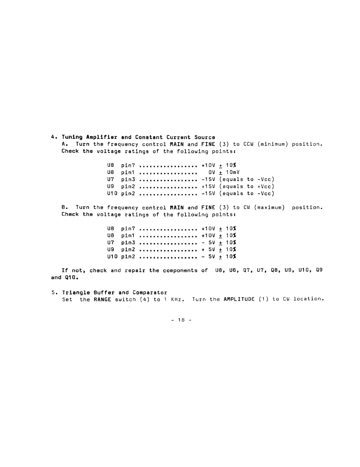
4.
Tuning
Amplifier
and
Constant
Current
Source
A.
Turn
the
frequency
control
MAIN
and
FINE
(3)
to
CCU
Check
the
voltage
ratings
of
the
following
points:
U8
pin?
U8
pin1
U7
pin3
U9
pin2
U10
pin2
.................
+1UV
.................
0V
.................
-15V
.................
+15V
ooooooooooooooooo
‘15"
8.
Turn
the
frequency
control
MAIN
and
FINE
Check
the
voltage
ratings
of
the
following
points:
UB
pin?
U8
pin1
U7
pin}
U9
pin2
U10
pin2
.................
+10V
.................
+10V
.................
-
5V
.................
+
5V
0.000.000.0000...
-
5"
If
not,
check
and
repair
the
components
of
and
Q10.
5.
Triangle
Buffer
and
Comparator
Set
the
RANGE
switch
(A)
to
1
KHz.
Turn
the
AMPLITUDE
(1)
to
CU
location.
i
10%
1
1DmV
(equals
to
(equals
to
(equals
to
(minimum)
position.
-Vcc)
+Vcc)
-Vcc)
(3)
to
cw
(maximum)
position.
10%
10%
101
10$
10%
l+|+|+l+l+
U8,
US,
07,
U7,
08,
U9,
U10,
09
4.
Tuning
Amplifier
and
Constant
Current
Source
A.
Turn
the
frequency
control
MAIN
and
FINE
(3)
to
CCU
(minimum)
position.
Check
the
voltage
ratings
of
the
following
points:
U8
pin?
U8
pin1
U7
pin3
U9
pin2
U10
pin2
B.
Turn
the
frequency
control
MAIN
and
+1UV
0V
-15V
+15V
—15V
.i...............
oocoaoo-Ioconcco-
pea-ooooo-uo'uoon-
IOOIIIICIOCCOOOCO
FINE
1
10%
i
1UmV
(equals
to
—Vcc)
(equals
to
+Vcc)
(equals
to
~Vcc)
(3)
to
CU
(maximum)
position.
Check
the
voltage
ratings
of
the
following
points:
ue
pin?
U8
pin1
U7
pin3
U9
pinZ
U10
pinz
If
not,
check
and
repair
the
components
and
Q10.
5.
Set
+1UV
+10V
—
5V
+
5V
-
5V
leoeoolooeoonooou
ole-conno-eluoool
nooooeoooooooooeo
IOIOIoIoo'Iooeell
of
Triangle
Buffer
and
Comparator
the
RANGE
switch
(4)
to
1
KHz.
_
18
_
l+|+t+l+i+
us,
101
10%
10%
105
101
U6,
U7,
U7,
08,
U9,
U10,
D9
Turn
the
AMPLITUDE
(1)
to
CU
location.
Check
and
be
sure
that
the
waveform
and
voltage
of
the
following
points:
013
Base
0000.00.00.00...
Av
ZVP-P
i
10%
,‘
U11
pin4
oooooooooooaoooo
I1
4.5Vp-p
i
10%
i
10%
ping
OOOOQGOOOODOEIOO
f1
3-5Vp”p
If
not,
check
and
repair
Q11,
Q13,
Q14
and.U11.
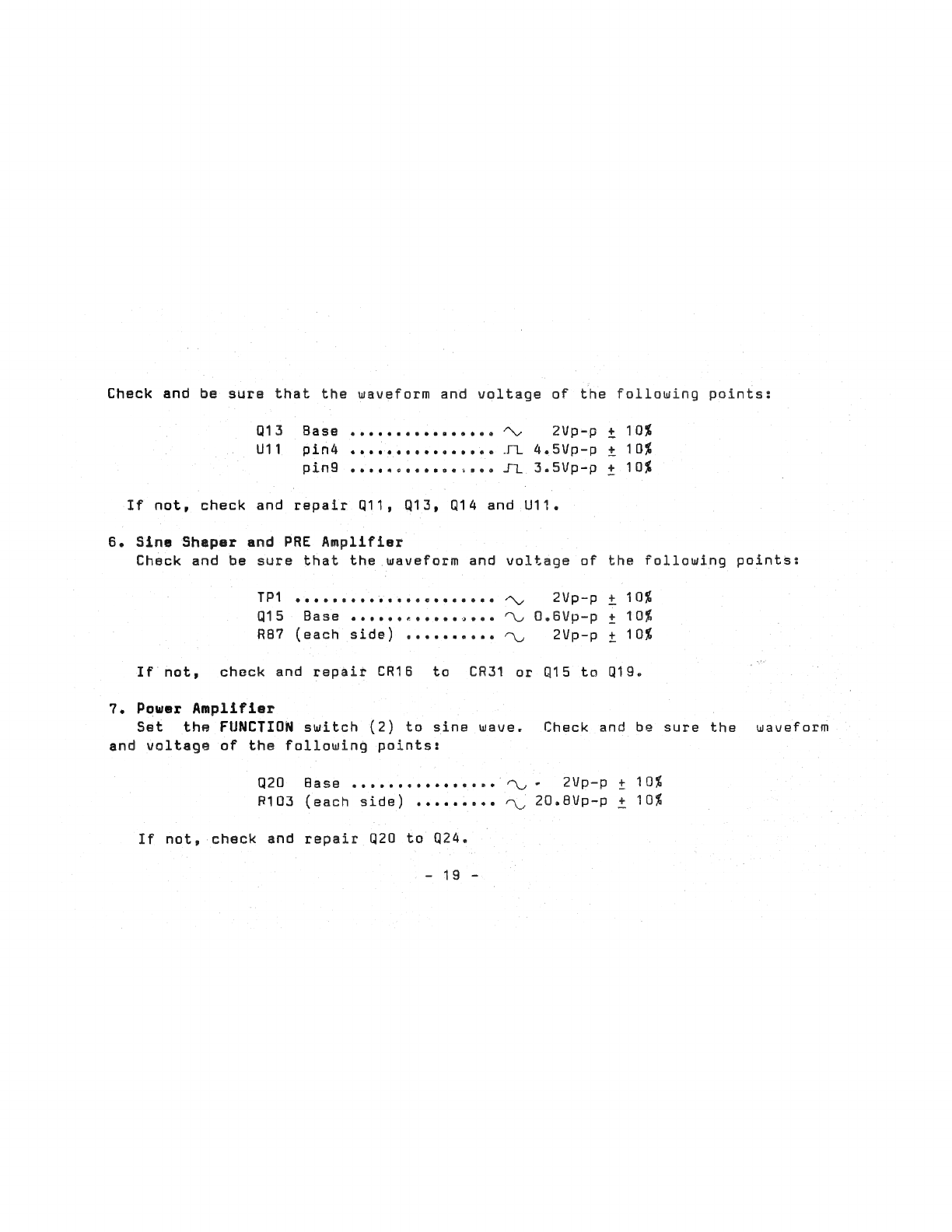
6.
Sine
Shape:
and
PRE
Amplifier
Check
and
be
sure
that
the
waveform
and
voltage
of
the
following
points:
Tp1
oooooooooooooooooooooo
AV
2Vp"p
:
10%
Q15
Base
0000006000069...
AU
UoBVp‘p
i
10%
R87
(eaCh
SidE)
00000-0...
AU
2Vp~p
:
10%
If
not,
check
and
repair
CR16
to
CR31
or
Q15
to
019.
7.
Power
Amplifier
Set
the
FUNCTION
switch
(2)
to
sine
wave.
Check
and
be
sure
the
waveform
and
voltage
of
the
following
points:
020
Base
ooooooooooooonoo‘fik,'
2Vp“p
:
10x
R103
(eaCh
Side)
.....a...
“V
ZUoBUp‘p
:
10%
If
not,
check
and
repair
020
to
024.
_
1g
_
Check
and
be
sure
that
the
waveform
and
voltage
of
the
following
points:
Q13
Base
ODDCIIIIIIIIOOODN
ZVp—pi'IUx
U11
pin4
concoucoooaavuoaJ—‘L
4.5Vp—p11DX
1
10%
pins
oooaasuonlnc;loo
I1
3.5Up-p
If
not,
check
and
repair
Q11,
Q13,
Q14
and
U11.
6.
Sins
Shepar
and
PRE
Amplifier
Check
and
be
sure
that
the
waveform
and
voltage
of
the
following
points:
TP1
onloooaoolI-ouaouaoooo
AV
2Vp‘p
:
10%
015
Base
.o.o..n.....a...”\JU.5Vp—p310%
R87
(Each
Side)
IOOIOIIOI.
nu
2Vp*p
i
10%
If
not.
check
and
repair
CR1B
to
CR31
or
G15
to
019.
7.
Power
Amplifier
Set
the
FUNCTION
switch
(2)
to
sine
wave.
Check
and
be
sure
the
waveform
and
voltage
of
the
following
points:
10%
10%
020
Base
CIIDDOOOIOOI‘IIOIN"
2Vp—p
R103
(each
side)
.........
av
20.8Vp-p
|+
1+
If
not,
check
and
repair
020
to
024.
_
1g
_
Table of contents
Popular Test Equipment manuals by other brands

Unit
Unit UT-P35 instruction manual

AutoTest
AutoTest AUTOSTOP Micro Plus user manual

Kyoritsu Electrical Instruments Works, Ltd.
Kyoritsu Electrical Instruments Works, Ltd. 4200 instruction manual

Unit
Unit UTD1025CL manual

Serveredge
Serveredge TRCER-CAB instruction manual

U.S. General
U.S. General 65928 Set up and operating instructions


