Toradex Colibri Guide

Colibri Computer Module
Carrier Board Design Guide

Colibri Carrier Board Design Guide
Toradex AG l Altsagenstrasse 5 l 6048 Horw l Switzerland l +41 41 500 48 00 l www.toradex.com l info@toradex.com
Page | 2
Issued by:
Toradex
Document Type:
Carrier Board Design Guide
Purpose:
This document is a guideline for developing a carrier board that confirms to the specifications
for the Colibri Computer Module
Document
Version:
1.7
Revision History
Date
Version
Remarks
13 Apr 2015
V1.0
Initial Release: Preliminary Version
28 Sept 2015
V1.1
Correct figure 3 and figure 4 in section 2.3.2 (positive and negative USB
signals were swapped in schematics)
22 Oct 2015
V1.2
Corrections in figure 4 in section 2.3.2 (pull up resistor of USB_OC# and
pull-down of USBH_EN where swapped)
Correction in typical pull-up value for I2C in section 2.9
15 Jun 2016
V1.3
Add section 2.1.4 "Pin Reset State"
Section 2.16: Updated information to the input voltage range
Section 2.17: Add a note to the usage of PXA270
Section 0: insert information to nVDD_FAULT, nGPIO_RESET, and
nBATT_SENSE
Section 3.6: Add information to bulk capacitors.
06 Apr 2017
V1.4
Section 2.2, Ethernet: Minor correction in figure 2
Section 2.5, HDMI/DVI: Correction in figure 12 (differential pair
impedance value)
All reference schematic images: Cosmetic update.
Section 1.2, Section 4 & Section 5: Updated web-links
14 Dec 2018
V1.5
Section 2.2.2: Add recommendation for ESD protection diodes
Section 2.3.1: Add note regarding default polarity of USB_H_PWR_EN
Section 2.3.2: Add USB OTG reference schematic
Section 2.3.2: Remove 15k pull down on USB data signals
Section 2.3.2.3: Change to the active low version of the power switch
(TPS2042 instead of TPS2052)
Section 2.15.3: Update recommendation for unused touch signals
Section 2.16.1: Correct pin numbers
05-Feb 2021
V1.6
Section 2.3.2.2: Update figure 4
Section 3.7: Add backfeeding recommendations

Colibri Carrier Board Design Guide
Toradex AG l Altsagenstrasse 5 l 6048 Horw l Switzerland l +41 41 500 48 00 l www.toradex.com l info@toradex.com
Page | 3
30-Apr 2021
V1.7
Section 2.19: Add module recovery description.
Section 3: Clarify module power requirement for supply design
Section 4.5: Add JTAG test pad description.
Minor changes

Colibri Carrier Board Design Guide
Toradex AG l Altsagenstrasse 5 l 6048 Horw l Switzerland l +41 41 500 48 00 l www.toradex.com l info@toradex.com
Page | 4
1Introduction................................................................................................................... 6
1.1 Overview............................................................................................................................. 6
1.2 Additional Documents .......................................................................................................... 6
1.2.1 Layout Design Guide.................................................................................................6
1.2.2 Colibri Module Datasheets.........................................................................................6
1.2.3 Toradex Developer Center.........................................................................................6
1.2.4 Colibri Evaluation Board Schematics ..........................................................................6
1.2.5 Pinout Designer ........................................................................................................7
1.3 Abbreviations....................................................................................................................... 7
2Interfaces...................................................................................................................... 9
2.1 Architecture......................................................................................................................... 9
2.1.1 Standard Interfaces...................................................................................................9
2.1.2 Interfaces on Alternative Functions.............................................................................9
2.1.3 Pin Numbering ........................................................................................................10
2.1.4 Pin Reset State.......................................................................................................10
2.2 Ethernet............................................................................................................................ 11
2.2.1 Ethernet Signals......................................................................................................11
2.2.2 Reference Schematics.............................................................................................11
2.2.3 Unused Ethernet Signals Termination.......................................................................12
2.3 USB.................................................................................................................................. 12
2.3.1 USB Signals ...........................................................................................................12
2.3.2 Reference Schematics.............................................................................................13
2.3.3 Unused USB Signal Termination ..............................................................................14
2.4 Parallel RGB LCD Interface................................................................................................ 14
2.4.1 Parallel RGB LCD Signals .......................................................................................15
2.4.2 Reference Schematics.............................................................................................15
2.4.3 Unused Parallel RGB Interface Signal Termination....................................................18
2.5 HDMI/DVI.......................................................................................................................... 18
2.5.1 HDMI/DVI Signals ...................................................................................................19
2.5.2 Reference Schematics.............................................................................................19
2.5.3 Unused HDMI/DVI Signal Termination......................................................................21
2.6 Analog VGA ...................................................................................................................... 22
2.6.1 VGA Signals ...........................................................................................................22
2.6.2 Reference Schematics.............................................................................................22
2.6.3 Unused VGA Interface Signal Termination................................................................23
2.7 Parallel Camera Interface................................................................................................... 23
2.7.1 Parallel Camera Signals ..........................................................................................23
2.7.2 Unused Parallel Camera Interface Signal Termination ...............................................24
2.8 SD/MMC/SDIO .................................................................................................................. 24
2.8.1 SD/MMC/SDIO Signals............................................................................................24
2.8.2 Reference Schematics.............................................................................................25
2.8.3 Unused SD/MMC/SDIO Interface Signal Termination.................................................25
2.9 I2C.................................................................................................................................... 25
2.9.1 I2C Signals..............................................................................................................25
2.9.2 Real-Time Clock (RTC) recommendation..................................................................25
2.9.3 Unused I2C Signal Termination.................................................................................26
2.10 UART................................................................................................................................ 26
2.10.1 UART Signals......................................................................................................26
2.10.2 Reference Schematics .........................................................................................27
2.10.3 Unused UART Signal Termination.........................................................................28
2.11 SPI ................................................................................................................................... 29
2.11.1 SPI Signals..........................................................................................................29
2.11.2 Unused SPI Signal Termination ............................................................................29
2.12 CAN.................................................................................................................................. 29
2.12.1 Reference Schematics .........................................................................................29

Colibri Carrier Board Design Guide
Toradex AG l Altsagenstrasse 5 l 6048 Horw l Switzerland l +41 41 500 48 00 l www.toradex.com l info@toradex.com
Page | 5
2.13 PWM................................................................................................................................. 30
2.13.1 PWM Signals.......................................................................................................30
2.13.2 Reference Schematics .........................................................................................30
2.13.3 Unused PWM Signal Termination..........................................................................30
2.14 Analog Audio..................................................................................................................... 31
2.14.1 Analog Audio Signals ...........................................................................................31
2.14.2 Reference Schematics .........................................................................................31
2.14.3 Unused Analog Audio Signal Termination..............................................................32
2.15 Touch Panel Interface ........................................................................................................ 33
2.15.1 Resistive Touch Signals .......................................................................................33
2.15.2 Reference Schematics .........................................................................................33
2.15.3 Unused Touch Panel Interface Signal Termination .................................................33
2.16 Analog Inputs .................................................................................................................... 34
2.16.1 Analog Input Signals ............................................................................................34
2.16.2 Unused Analog Inputs Signal Termination .............................................................34
2.17 Parallel Memory Bus (External Memory Bus)....................................................................... 34
2.17.1 Memory Bus Signals ............................................................................................34
2.17.2 Unused Memory Bus Signals Termination .............................................................36
2.18 GPIO ................................................................................................................................ 36
2.18.1 Preferred GPIO Signals........................................................................................36
2.18.2 Unused GPIO Termination....................................................................................36
2.19 Module Recovery............................................................................................................... 37
3Power Management....................................................................................................... 38
3.1 Power Supply Design......................................................................................................... 38
3.2 Power Signals ................................................................................................................... 38
3.2.1 Digital Supply Signals..............................................................................................38
3.2.2 Analog Supply Signals.............................................................................................38
3.2.3 Power Management Signals ....................................................................................39
3.3 Power Block Diagram......................................................................................................... 39
3.4 Power States..................................................................................................................... 41
3.5 Power-Up Sequence.......................................................................................................... 41
3.6 Reference Schematics ....................................................................................................... 42
3.7 Backfeeding ...................................................................................................................... 44
3.7.1 Introduction.............................................................................................................44
3.7.2 What is Backfeeding................................................................................................44
3.7.3 Potential Issues Caused by Backfeeding...................................................................46
3.7.4 Identify Backfeeding Issues......................................................................................47
3.7.5 Backfeeding Prevention...........................................................................................50
4Mechanical and Thermal Consideration ........................................................................... 60
4.1 Module Connector.............................................................................................................. 60
4.2 Fixation of the Module........................................................................................................ 60
4.3 Thermal Solution................................................................................................................ 62
4.4 Module Size ...................................................................................................................... 62
4.5 JTAG Test Pads ................................................................................................................ 63
5Appendix A –Physical Pin Definition and Location ............................................................ 64

Colibri Carrier Board Design Guide
Toradex AG l Altsagenstrasse 5 l 6048 Horw l Switzerland l +41 41 500 48 00 l www.toradex.com l info@toradex.com
Page | 6
1 Introduction
1.1 Overview
This document guides the development of a customized carrier board for the Colibri computer
module. It describes the different interfaces and contains reference schematics. This document
reflects only the standardized primary function of the Colibri modules. The alternative functions are
not guaranteed to be compatible between different Colibri modules. These interfaces are described
in the datasheet of each computer module. Some Colibri modules do not feature the complete set
of standard interfaces. Therefore, it is strongly recommended to read the datasheets of the
modules that are intended to be used with the carrier board.
Some of the Colibri computer module interfaces, such as High-Speed USB and Ethernet, require
special layout considerations regarding trace impedance and length matching. Please carefully
read the Toradex Layout Design Guide for additional information related to the routing of these
interfaces.
1.2 Additional Documents
1.2.1 Layout Design Guide
This document contains layout requirement specifications for the high-speed signals and avoids
problems related to the layout.
http://developer.toradex.com/carrier-board-design/carrier-board-design-guides
1.2.2 Colibri Module Datasheets
There is a datasheet available for every Colibri module. Amongst other things, this document
describes the type-specific interfaces and the alternative function of the pins. Before starting the
development of a customized carrier board, please check this document to determine whether the
required interfaces are available on the selected modules.
https://www.toradex.com/computer-on-modules/colibri-arm-family
1.2.3 Toradex Developer Center
You can find a lot of additional information at the Toradex Developer Center, which is updated
with the latest product support information regularly.
Please note that the Developer Center is common for all Toradex products. You should always
check to ensure if the information is valid or relevant for the specific Colibri modules.
http://www.developer.toradex.com
1.2.4 Colibri Evaluation Board Schematics
We provide the complete schematics plus the Altium project file for the Colibri Evaluation Board for
free. This is a great help when designing your own Carrier Board.
http://developer.toradex.com/products/colibri-evaluation-board

Colibri Carrier Board Design Guide
Toradex AG l Altsagenstrasse 5 l 6048 Horw l Switzerland l +41 41 500 48 00 l www.toradex.com l info@toradex.com
Page | 7
1.2.5 Pinout Designer
This is an interactive and helpful tool for configuring the pin muxing of the Colibri and Apalis
modules. It can be beneficial in custom carrier board development for Toradex modules and for
checking the compatibility of existing carrier boards with our modules.
http://developer.toradex.com/carrier-board-design/pinout-designer-tool
1.3 Abbreviations
Abbreviation
Explanation
ADC
Analog to Digital Converter
AGND
Analog Ground - separate ground for analog signals
Auto-MDIX
Automatically Medium Dependent Interface Crossing - a PHY with Auto-MDIX it can detect whether RX
and TX need to be crossed (MDI or MDIX)
CAD
Computer-Aided Design –in this document it is referred to PCB Layout tools
CAN
Controller Area Network - a bus that is manly used in the automotive and industrial environment
CDMA
Code Division Multiplex Access - abbreviation often used for a mobile phone standard for data
communication
CEC
Consumer Electronic Control - HDMI feature that allows controlling CEC compatible devices
CPU
Central Processor Unit
CSI
Camera Serial Interface
DAC
Digital to Analog Converter
DDC
Display Data Channel - interface for reading out the capability of a monitor. In this document DDC2B
(based on I2C) is always meant
DRC
Design Rule Check - a tool for checking whether all design rules are satisfied in a CAD tool
DSI
Display Serial Interface
DVI
Digital Visual Interface - digital signals are electrically compatible with HDMI
DVI-A
Digital Visual Interface Analog only - signals are compatible with VGA
DVI-D
Digital Visual Interface Digital only - signals are electrically compatible with HDMI
DVI-I
Digital Visual Interface Integrated - combines digital and analog video signals in one connector
EDA
Electronic Design Automation - software for schematic capture and PCB layout (CAD or ECAD)
EDID
Extended Display Identification Data - timing setting information provided by the display in a PROM
EMI
Electromagnetic Interference - high-frequency disturbances
eMMC
Embedded Multi Media Card - flash memory combined with MMC interface controller in a BGA package,
used as internal flash memory
ESD
Electrostatic Discharge - high voltage spike or spark that can damage electrostatic- sensitive devices
FPD-Link
Flat Panel Display Link - high-speed serial interface for liquid crystal displays. In this document, it is also
called the LVDS interface.
GBE
Gigabit Ethernet - Ethernet interface with a maximum data rate of 1000Mbit/s
GND
Ground
GPIO
General Purpose Input/Output pin that can be configured to be either an input or output
GSM
Global System for Mobile Communications
HDA
High Definition Audio (HD Audio) - a digital audio interface between CPU and audio codec
HDCP
High-Bandwidth Digital Content Protection - copy protection system that is used by HDMI beside others
HDMI
High-Definition Multimedia Interface - combines audio and video signal for connecting monitors, TV sets
or Projectors, electrical compatible with DVI-D
I2C
Inter-Integrated Circuit - two-wire interface for connecting low-speed peripherals
I2S
Integrated Interchip Sound - serial bus for connecting PCM audio data between two devices
IrDA
Infrared Data Association - infrared interface for connecting peripherals
JTAG
Joint Test Action Group - widely used debug interface
LCD
Liquid Crystal Display
LSB
Least Significant Bit
LVDS
Low-Voltage Differential Signaling - electrical interface standard that can transport very high-speed
signals over twisted-pair cables. Many standard interfaces like PCIe or SATA use this interface standard.

Colibri Carrier Board Design Guide
Toradex AG l Altsagenstrasse 5 l 6048 Horw l Switzerland l +41 41 500 48 00 l www.toradex.com l info@toradex.com
Page | 8
Abbreviation
Explanation
Since the first successful application was the Flat Panel Display Link, LVDS has become synonymous
with this interface. In this document, the term LVDS is used for the FPD-Link interface.
MIPI
Mobile Industry Processor Interface Alliance
MDI
Medium Dependent Interface - a physical interface between Ethernet PHY and cable connector
MDIX
Medium Dependent Interface Crossed - an MDI interface with crossed RX and TX interfaces
mini PCIe
PCI Express Mini Card - card form factor for internal peripherals. The interface features PCIe and USB
2.0 connectivity
MMC
MultiMediaCard - flash memory card
MSB
Most Significant Bit
mSATA
Mini-SATA - a standardized form factor for small solid-state drive, similar dimensions as mini PCIe
N/A
Not Available
N/C
Not Connected
OD
Open-Drain
OTG
USB On-The-Go - a USB host interface that can also act as a USB client when connected to another host
interface
OWR
One Wire (1-Wire) - a low-speed interface that needs just one data wire plus ground
PCB
Printed Circuit Board
PCI
Peripheral Component Interconnect - parallel computer expansion bus for connecting peripherals
PCIe
PCI Express - high-speed serial computer expansion bus, replaces the PCI bus
PCM
Pulse-Code Modulation - digital representation of analog signals and a standard interface for digital audio
PD
Pull Down Resistor
PHY
Physical Layer of the OSI model
PMIC
Power Management IC - integrated circuit that manages amongst others the power sequence of a system
PU
Pull-up Resistor
PWM
Pulse-Width Modulation
RGB
Red Green Blue - color channels in standard display interfaces
RJ45
Registered Jack - common name for the 8P8C modular connector that is used for Ethernet wiring
RS232
Single-ended serial port interface
RS422
Differential signaling serial port interface - full-duplex
RS485
Differential signaling serial port interface - half-duplex, multi-drop configuration possible
R-UIM
Removable User Identity Module - identifications card for CDMA phones and networks, an extension of
the GSM SIM card
S/PDIF
Sony/Philips Digital Interconnect Format - optical or coaxial interface for audio signals
SATA
Serial ATA, high-speed differential signaling interface for hard drives and SSD
SD
Secure Digital - flash memory card
SDIO
Secure Digital Input Output - an external bus for peripherals that uses the SD interface
SIM
Subscriber Identification Module - identification card for GSM phones
SMBus
System Management Bus (SMB) - a two-wire bus based on the I2C specifications, used mainly in x86
design for system management.
SoC
System on a Chip - IC which integrates the main component of a computer on a single chip
SO-DIMM
Small Outline Dual Inline Memory Module - form factor for mobile RAM modules, the Colibri module uses
the SO-DIMM (DDR, 2.5V variant) connector as the primary interface
SPI
Serial Peripheral Interface Bus - synchronous four-wire full-duplex bus for peripherals
TIM
Thermal Interface Material - thermal conductive material between CPU and heat spreader or heat sink
TMDS
Transition-Minimized Differential Signaling - serial high-speed transmitting technology that is used by DVI
and HDMI
TVS Diode
Transient-Voltage-Suppression Diode - diode that is used to protect interfaces against voltage spikes
UART
Universal Asynchronous Receiver/Transmitter - serial interface, in combination with a transceiver an
RS232, RS422, RS485, IrDA, or similar interface can be achieved
USB
Universal Serial Bus - serial interface for internal and external peripherals
VCC
Positive supply voltage
VGA
Video Graphics Array - analog video interface for monitors
Table 1: Abbreviations

Colibri Carrier Board Design Guide
Toradex AG l Altsagenstrasse 5 l 6048 Horw l Switzerland l +41 41 500 48 00 l www.toradex.com l info@toradex.com
Page | 9
2 Interfaces
2.1 Architecture
2.1.1 Standard Interfaces
The Colibri module family's standard interfaces intend to provide electrical and functional
compatibility between module family members. The table below shows an overview of the
standard interfaces that are provided by a Colibri module. The "GPIO Capable" column indicates
whether the assigned pins intend to be also used as GPIOs. "Yes" and "No" are self-Explanatory.
"Optional" indicates that it may be possible for some modules, but not all.
The "Standard" column indicates the number of interfaces that the specification allows for the
standard pinout. Customers should consult the datasheet for specific Colibri module variants to
check which of the interfaces are available for that module.
Description
Standard
Note
GPIO
Capable
4/5 Wire Resistive Touch
1
Touch wiper shared with analog input 4
No
Analog Inputs
4
Minimum 8-bit resolution, 0-3.3V nominal range
No
Analog Audio
1
Line in L&R, Microphone in, Headphone out L&R
No
Fast Ethernet
1
No
HDMI (TDMS)
1
Located on a dedicated FFC connector
(availability depending on Module)
No
I2C
1
Additional dedicated DDC available on FFC connector
Yes
Parallel Camera
1
8-bit BT.656 (other modes may be available)
Yes
Parallel LCD
1
18-bit resolution (additional bits may be available)
Yes
Parallel Memory Bus
1
Supported bus width depends on Module
Optional
PWM
4
Yes
SDIO
1
4 bit
Yes
SPI
1
Yes
UART
3
1x Full Featured, 1x CTS/RTS, 1x RXD/TXD only
Yes
USB
2
1x shared host/client, 1x host only
No
VGA
1
Located on a dedicated FFC connector
(availability depending on Module)
No
Table 2: Standard Interfaces
2.1.2 Interfaces on Alternative Functions
Many SoC pins can be used for more than one function. This allows the modules to provide many
additional interfaces to the standard set. For example, in the Colibri standard, there is only one SPI
interface listed. Nevertheless, some modules can provide up to 6 SPI interfaces.
Please note that there are a few restrictions on using the interfaces provided as alternative
functions of the pins. There is limited compatibility between their availability at different modules.
For a design to be compatible with a wide range of Colibri modules, it is recommended to use the
standard interfaces mainly. The various pins can be used for only one function simultaneously.
The configuration of the alternative function interfaces can be pretty complex. Toradex provides a
powerful tool that helps the development engineer to resolve pin muxing conflicts. The tool is
called Pinout Designer. It reduces the complexity of this critical task. More information, including its
download link, can be found here:
http://developer.toradex.com/carrier-board-design/pinout-designer-tool

Colibri Carrier Board Design Guide
Toradex AG l Altsagenstrasse 5 l 6048 Horw l Switzerland l +41 41 500 48 00 l www.toradex.com l info@toradex.com
Page | 10
The interfaces on the alternative functions are not described in this document since they differ
between the modules. Information related to these functions can be found in the datasheets of the
modules.
2.1.3 Pin Numbering
The diagrams in the figures below show the pin numbering schema on both sides of the module.
The schema is equal to the JEDEC MO-224 DDR SO-DIMM standard. The odd pin numbers are
located on the top side of the module.
Figure 1: Colibri Module Pin Numbering Schema
2.1.4 Pin Reset State
The datasheets of the Colibri module provide information about the default reset status of the IO
pins. Please be aware that the pin reset status is only guaranteed during the release of the reset
signal. Some of the modules switch the IO bank voltages to follow the power-up sequence of the
SoC. This means the IO pins can have an undefined state between applying the main power to the
module until the nRESET_OUT is released. For carrier board designs that do not allow undefined
pin states, it is recommended to ensure that the peripheral devices are not powered before the
nRESET_OUT is released. Another solution can be gating the related IO signals with the
nRESET_OUT signal.
Pin1 Pin47Pin39 Pin199
Pin2 Pin42Pin40 Pin200
Colibri Carrier Board Design Guide
Toradex AG l Altsagenstrasse 5 l 6048 Horw l Switzerland l +41 41 500 48 00 l www.toradex.com l info@toradex.com
Page | 11
2.2 Ethernet
The Colibri module standard features a fast 10/100Mbit Ethernet (10/100Base-TX) interface port.
The required center tap circuit can differ between the modules. Different assembly options might
be needed for supporting the complete Colibri module family. Some modules support Auto MDIX,
which means they can swap the transmitting with the receiving lanes. Read the corresponding
datasheet of the module for more information about the availability of the Auto MDIX function.
2.2.1 Ethernet Signals
Colibri
Pin
Colibri
Signal Name
I/O
Type
Power
Rail
Description
189
ETH_1_TXO+
I
Analog
100BASE-TX: Transmit + (Auto MDIX: Receive +)
187
ETH_1_TXO-
I
Analog
100BASE-TX: Transmit - (Auto MDIX: Receive -)
195
ETH_1_RXI+
O
Analog
100BASE-TX: Receive + (Auto MDIX: Transmit +)
193
ETH_1_RXI-
O
Analog
100BASE-TX: Receive - (Auto MDIX: Transmit -)
191
AGND_LAN
Ethernet ground, on some modules connected to common GND
183
ETH_1_LINK_AKT
O
CMOS
3.3V
LED indication output for link activity on the Ethernet port
185
ETH_1_SPEED100
O
CMOS
3.3V
LED indication output for 100Mbit/s
Table 3: Ethernet Signals
2.2.2 Reference Schematics
Ethernet connectors with integrated magnetics are preferable. If a design with external magnetics
is chosen, additional care must be taken to route the signals between the magnetics and Ethernet
connector.
The LED output signals ETH_1_LINK_AKT and ETH_1_SPEED100 can be connected directly to the
LED of the Ethernet jack with suitable serial resistors. There is no need for additional buffering if
the current drawn does not exceeds 10mA.
The Fast Ethernet interface uses the ETH_1_TXO as transmitting lanes and the ETH_1_RXI as
receiving lane. If the Ethernet PHY features Auto-MDIX, the signal lanes RX and TX could be
swapped. We strongly recommend not swapping the RX and TX lanes to keep the compatibility with
all Colibri modules.
The required center tap circuit depends on the supported modules. Currently, the Ethernet
controller on the PXA270 module is the only one that requires a different center tap circuit since it
does not support Auto-MDIX. All the other currently available modules feature a current control
PHY that requires a 3.3V supply at the center tap of the RX and TX lanes. Since all the Ethernet PHY
manufacturers are tending to change from current mode to voltage mode, which requires leaving
the center tab pins of the magnetics unconnected, we recommend adding additional 0R resistors
into the center tab lines. This ensures that the carrier board design is ready for any future Colibri
module with voltage-mode PHY.
The magnetics provide a certain ESD protection which is sufficient for many designs. However,
especially in Power over Ethernet (PoE) systems, additional transient voltage suppressor diodes
(TVS) are highly recommended between the module and the magnetics. More information can be
found in the following application note from Microchip:
http://ww1.microchip.com/downloads/en/AppNotes/00002157B.pdf

Colibri Carrier Board Design Guide
Toradex AG l Altsagenstrasse 5 l 6048 Horw l Switzerland l +41 41 500 48 00 l www.toradex.com l info@toradex.com
Page | 12
Figure 2: Fast Ethernet with Integrated Magnetics Reference Schematic
2.2.3 Unused Ethernet Signals Termination
All unused Ethernet signals can be left unconnected.
2.3 USB
The Colibri modules feature two USB interfaces. One of the two USB interfaces can be configured
to be used as either the host or client. The other interface can only be used as a host. Some of the
Colibri modules use the USB client port for debugging and recovery purposes. Therefore, it is
recommended to have the interface accessible even for carrier board designs that do not need any
USB ports.
2.3.1 USB Signals
Colibri
Pin
Colibri
Signal Name
I/O
Type
Power
Rail
Description
139
USB_H_DP
I/O
USB
3.3V
Positive Differential Signal for USB Host port
141
USB_H_DM
I/O
USB
3.3V
Negative Differential Signal for USB Host port
143
USB_C_DP
I/O
USB
3.3V
Positive Differential Signal for the shared USB Host / Client port
145
USB_C_DM
I/O
USB
3.3V
Negative Differential Signal for the shared USB Host / Client port
Table 4: USB Data Signals
If you use the USB Host function, you need to generate the 5V USB supply voltage on your carrier
board. The Colibri modules provide two optional signals for USB power supply control (PWR_EN
and OC). We recommend using the following pins to ensure the best possible compatibility.
However, the use of these signals is not mandatory, and other GPIOs may be used instead.
In the USB client mode, an additional signal is required that detects whether the client is connected
to a host interface (VBUS_DETECT). Please note that this pin is only 3.3V tolerant. Therefore, an
additional logic level shifter (the simplest solution is a voltage divider) is required.
Colibri
Pin
Colibri
Signal Name
I/O
Type
Power
Rail
Description
129
USB_H_PWR_EN
O
CMOS
3.3V
This pin enables the external USB voltage supply. By default, this
pin is active low.
131
USB_H_OC
I
CMOS
3.3V
USB overcurrent, this pin can signal an overcurrent condition in the
USB supply
137
USB_C_VBUS_DETECT
I
CMOS
3.3V
Use this pin to detect if VBUS is present (5V USB supply). Please
note that this pin is only 3.3V tolerant
Table 5: USB Control Signals
ETH_LINK_ACT
ETH_SPEED
ETH_TX 0_N
ETH_TX 0_P
ETHERNET[0..5]
50R
R20
50R
R21
100nF
16VC45
GND
50R
R22
50R
R23
100nF
16VC46
GND
ETH_RX I_P
ETH_RX I_N
C44
100nF
16V
GND
ETH_AVCC
3.3V
3.3V
2A
220R@ 100MHz
L10
47uF
6.3V
+
C4 8
47uF
6.3V
+
C49
3.3V ETH_AVCC
GND
150 RR25
150RR24
J00- 0065N L
TD +
1
TD -
2
CT_TX D
4
CT_RX D
5
RD +
3
RD -
6
LED_Left_ A
9
LED_Left_ C
10
LED_R ight_ C
11 LED_R ight_ A
12 SHIELD S1
SHIELD S2
NC 7
CHS GND 8
X17
ETH_LINK_ACT
ETH_SPEED
ETH_TX0_N
ETH_TX0_P
ETH_RXI_N
ETH_RXI_P
1473005 -1
ETH_LINK_ACT 183
ETH_SPEED 185
ETH_TX0-
ETH_TX0+ 189
ETH_RXI- 193
ETH_RXI+ 195
ETH_GND 191
Colibri -Ethernet
2of 16
X1B
SHIELD
Ethernet Connector
ETH_CT_TX
ETH_CT_RX
GND
GND
0R
R10
C47
100nF
16V
GND
0R
R11
0R
R12
NA
PXA2700RNA0R
ModuleR12R11R10
All except PXA2700RNA 0R
Reserved for future modulesNA NANA (Integrated Magnetics)
187
Colibri Carrier Board Design Guide
Toradex AG l Altsagenstrasse 5 l 6048 Horw l Switzerland l +41 41 500 48 00 l www.toradex.com l info@toradex.com
Page | 13
2.3.2 Reference Schematics
2.3.2.1 USB 2.0 Client Schematic Example
The differential USB data signals require a common mode choke to be placed. Make sure that the
selected choke is certified for USB 2.0 High Speed. The same is also required for the TVS diodes.
The VBUS_DETECT signal is only 3.3V tolerant on the Colibri module. The simplest solution is to
use a voltage divider.
Figure 3: USB 2.0 Client Reference Schematic
2.3.2.2 USB 2.0 OTG Schematic Example
The Colibri standard does not support the full USB OTG function. However, it is possible to
implement a circuit on the carrier board that allows changing the role from host to client
depending on the level of the ID pin of a Micro-AB jack. The reference schematic differs from other
USB OTG solutions since the module itself does not directly use the ID pin to detect whether the
port is supposed to be set in client or host mode. The pin is indirectly used.
If no cable is plugged into the Micro-AB jack, the port is configured to host mode, and the 5V
power output (VCC_USB2 in the schematic below) is disabled. If a Micro-B is plugged in (ID pin is
floating on such plugs), the VCC_USB2 comes from the cable since the system gets plugged into a
host. With the help of the voltage divider, the USB_C_DET signal gets around 3.3V. This signalizes
the module that it has been connected to a host and needs to switch to client mode.
If a Micro-A connector is inserted, the ID pin gets shorted to the ground. This ID pin enables the
output of the TPS2042 power switch. This voltage on the VCC_USB2 rail is used to power any client
device connected to the port. Additionally, the ID pin keeps the USB_C_DET signal low over a
diode, even though the VCC_USB2 rail goes to 5V. This makes sure the module remains in host
mode to be able to communicate with the client device that is plugged in.
Figure 4: USB 2.0 OTG Reference Schematic
GND
2A
220R@100MHz
L1
90R@100MHz
1
2 3
4
L2
USBO1_D_N
USBO1_D_P USBO1_D_CON_N
USBO1_D_CON_P
330R
R3
GND
GREEN
LED1
SHIELD
VCC_USBO1
VCC_USBO1
GND_USBO1
Optional
USBO1_VBUS
RCLAMP0504S
1
2
3 4
5
6
D1
4A
39R@100MHz
L3
100nF
C1
SHIELD
5V_ESD
SHIELD
5V
VCC
1
D-
2
D+
3
GND
4S1
S2
61729-0010BLF
X2
1473005-1
USBH_P 139
USBH_N 141
USBC_P 143
USBC_N 145
PIN_131/USB_OC 131
PIN_137/USBC_CABLEDET 137
PIN_129/USB_P_EN 129
Colibri - USB
3 of 16
X1C
560R
R73
R74
1K
GND
GND
5V R50
100K
3.3V
USBC_P
USBC_N
GND
90R@100MHz
1
2 3
4
L15
220R@100MHz
2A
L18
100nF
16V
C43
GND
3.3V
USB_ID
R61
100K
TPS2042BD
GND
1V_IN
2
EN_1#
3
EN_2#
4
OC_2# 5
OUT_2 6
OUT_1 7
OC_1# 8
IC1
RCLAMP0504S
1
2
34
5
6
D11
100nF
16V
C104
560R
R115
R116
1K
GND
GND
GND
USB_ID
1473005-1
USBH_P 139
USBH_N 141
USBC_P 143
USBC_N 145
PIN_131/USB_OC 131
PIN_137/USBC_CABLEDET 137
PIN_129/USB_P_EN 129
Colibri - USB
3 of 16
X1C
USB_CLIENT_N
USB Host / Client
Micro-AB type
22uF
10V
C42
GND
VBUS
USB_CLIENT_P
BAT54C
D12B
ZX62-AB-5PA(31)
VCC
1
D-
2
D+
3
ID
4
GND
5
S1
S3
S2
X12
Alternative part for connector X12:
-TE/Tyco,1981584-1
CHASSIS_GND
1nF
2KV
C129 R37
1M
GND
USB_OC
USB_ID
USB_C_DET
3.3V
VBUS
USB_OC
Colibri Carrier Board Design Guide
Toradex AG l Altsagenstrasse 5 l 6048 Horw l Switzerland l +41 41 500 48 00 l www.toradex.com l info@toradex.com
Page | 14
2.3.2.3 USB 2.0 Host Connector Schematic Example
The carrier board needs to provide 5V USB bus power on the USB host jacks. According to the USB
2.0 specifications, the maximum current drawn per port is limited by 500mA. The bus power needs
to be in the range of 4.75V to 5.25V measured at the USB host jack for any load current from 0mA
to 500mA. To ensure that an out-of-spec device or a defective device is not damaging the 5V
power rail on the carrier board, adding a current limiting IC is recommended. This device detects
an overcurrent situation and switches off the corresponding USB bus power. The overcurrent signal
(USB_H_OC) is used to notify the host controller about the occurrence of an overcurrent shutdown
event.
The inrush current needs to be taken into account while designing the USB bus power. USB devices
are allowed to have a maximum input capacitor at the bus power of 10µF. The maximum inrush
charge is limited to 50µC. This means that the power rail at the USB host jack needs to be tolerant
of this inrush current. A good approach is to place a large capacitor (e.g., 100µF) at the rail.
Figure 5: USB 2.0 Host Reference Schematic
2.3.3 Unused USB Signal Termination
Colibri
Pin
Colibri
Signal Name
Recommended Termination
139
USB_H_DP
Leave NC if not used
141
USB_H_DM
Leave NC if not used
143
USB_C_DP
Leave NC if not used
145
USB_C_DM
Leave NC if not used
129
USB_H_PWR_EN
Leave NC if not used
131
USB_H_OC
Add pull-up resistor or disable the overcurrent function in software
137
USB_C_VBUS_DETECT
Leave NC if not used
Table 6: Unused USB Signals Termination
2.4 Parallel RGB LCD Interface
The Colibri modules feature one parallel RGB LCD interface as the primary display interface. As
standard, the Colibri modules feature an interface with 18-bit color depth. Some modules support
a color depth of 16-bit or 24-bit. Unfortunately, the color mapping of these modes can be different
between the modules. Therefore, Toradex recommends using the interface in the 18-bit color
mode for the best compatibility between all Colibri modules. Dithering can help to reduce the
visible color banding of gradients in lower color depth systems. Consider using 18-bit color
mapping with enabled dithering instead of 24-bit mapping. Carefully check which modules support
color dithering.
2A
220R@100MHz
L3 1nF
50V
C3
GND_USBH
100nF
16V
C1
GND
100uF
10V
+
C2
GND
GND
2A
220R@100MHz
L2
90R@100MHz
1
2 3
4
L1
USBH2_D_N
USBH2_D_P USBH2_D_CON_N
USBH2_D_CON_P
330R
R1
GND
GREEN
LED1
TPD2EUSB30DRTR
12 D+D-
D2
GND
SHIELD
VCC_USBH VCC_USBH
USBH_OC#
USBH_EN#
GND_USBH
Optional
USBH_OC#
USBH_EN#
GND
5V
VCC
1
D-
2
D+
3
GND
4
292303-1
S1
S2
S3
S4
X2
R2
100K
3.3V
R3
100K
GND
1473005-1
USBH_P 139
USBH_N 141
USBC_P 143
USBC_N 145
PIN_131/USB_OC 131
PIN_137/USBC_CABLEDET 137
PIN_129/USB_P_EN 129
Colibri - USB
3 of 16
X1C
TPS2042BD
GND
1
V_IN
2
EN_1#
3
EN_2#
4
OC_2#
5OUT_2 6
OUT_1 7
OC_1#
8
IC?
3.3V

Colibri Carrier Board Design Guide
Toradex AG l Altsagenstrasse 5 l 6048 Horw l Switzerland l +41 41 500 48 00 l www.toradex.com l info@toradex.com
Page | 15
2.4.1 Parallel RGB LCD Signals
Colibri
Pin
Colibri
Signal Name
I/O
Type
Power
Rail
Description
52
LCD_1_18bit_R0
O
CMOS
3.3V
Red LCD data signals (LSB: 0, MSB: 5)
54
LCD_1_18bit_R1
O
CMOS
3.3V
66
LCD_1_18bit_R2
O
CMOS
3.3V
64
LCD_1_18bit_R3
O
CMOS
3.3V
57
LCD_1_18bit_R4
O
CMOS
3.3V
61
LCD_1_18bit_R5
O
CMOS
3.3V
80
LCD_1_18bit_G0
O
CMOS
3.3V
Green LCD data signals (LSB: 0, MSB: 5)
46
LCD_1_18bit_G1
O
CMOS
3.3V
62
LCD_1_18bit_G2
O
CMOS
3.3V
48
LCD_1_18bit_G3
O
CMOS
3.3V
74
LCD_1_18bit_G4
O
CMOS
3.3V
50
LCD_1_18bit_G5
O
CMOS
3.3V
76
LCD_1_18bit_B0
O
CMOS
3.3V
Blue LCD data signals (LSB: 0, MSB: 5)
70
LCD_1_18bit_B1
O
CMOS
3.3V
60
LCD_1_18bit_B2
O
CMOS
3.3V
58
LCD_1_18bit_B3
O
CMOS
3.3V
78
LCD_1_18bit_B4
O
CMOS
3.3V
72
LCD_1_18bit_B5
O
CMOS
3.3V
44
LCD_1_18bit_DE
O
CMOS
3.3V
Data Enable (other names: Output Enable)
56
LCD_1_18bit_PCLK
O
CMOS
3.3V
Pixel Clock (other names: Dot Clock, L_PCLK_WR)
68
LCD_1_18bit_HSYNC
O
CMOS
3.3V
Horizontal Sync (other names: Line Clock, L_LCKL_A0)
82
LCD_1_18bit_VSYNC
O
CMOS
3.3V
Vertical Sync (other names: Frame Clock, L_FCLK)
Table 7: Parallel RGB LCD Signals
2.4.2 Reference Schematics
2.4.2.1 18-bit Display Schematic Example
The parallel RGB interface can cause problems in passing the electromagnetic radiation tests when
used with high pixel clock frequency, especially if a display is connected over long flat flex cables.
The reduction of radiation needs to be taken into account. Keep the flat flex cables as short as
possible. Series resistors in the data lines reduce the slew rate of the signals, which reduces the
radiation problem but can introduce signal quality and timing problems. The serial resistor value is
a trade-off between electromagnetic radiation reduction and signal quality. A good starting value
is 22Ω.
Colibri Carrier Board Design Guide
Toradex AG l Altsagenstrasse 5 l 6048 Horw l Switzerland l +41 41 500 48 00 l www.toradex.com l info@toradex.com
Page | 16
Figure 6: 18bit Parallel RGB Display Reference Schematic
2.4.2.2 VGA DAC Schematic Example
A few Colibri modules feature a dedicated VGA interface on an FFC connector. Nevertheless,
adding a parallel RGB to VGA converter is recommended if a VGA interface is needed, which is
compatible with all modules. Since only the 18-bit color depth is compatible between the different
modules, it is recommended to use this mode even if the DAC is capable of 24-bit.
Figure 7: VGA DAC Reference Schematic

Colibri Carrier Board Design Guide
Toradex AG l Altsagenstrasse 5 l 6048 Horw l Switzerland l +41 41 500 48 00 l www.toradex.com l info@toradex.com
Page | 17
2.4.2.3 LVDS Transmitter Schematic Example
Since the electromagnetic radiation of the parallel RGB interface is not easy to handle, it is
recommended to attach liquid crystal displays with high resolutions by using an LVDS interface.
LVDS also reduces problems associated with long cables. The Colibri standard does not feature a
dedicated LVDS LCD interface. Nevertheless, a parallel RGB to LVDS transmitter can be placed on
the carrier board to get an LVDS interface.
Since there are different LVDS color mapping available, check with your display vendor how the
RGB signals need to be connected to the transmitter in order to be compatible.
Figure 8: LVDS Transmitter Reference Schematic
18-bit Color Mapping
The color mapping for the 18-bit LVDS interface is standardized and is shown in the following
picture:
Figure 9: 18-bit LVDS Color Mapping
LVDS1_A_CLK+
LVDS1_B_CLK+
LVDS1_A_TX0+/-
LVDS1_B_TX0+/-
LVDS1_A_TX1+/-
LVDS1_B_TX1+/-
LVDS1_A_TX2+/-
LVDS1_B_TX2+/-
Previous Cycle Current Cycle Next Cycle
G0 R5 R4 R3 R2 R1 R0
B1 B0 G5 G4 G3 G2 G1
DE VSYNC HSYNC B5 B4 B3 B2

Colibri Carrier Board Design Guide
Toradex AG l Altsagenstrasse 5 l 6048 Horw l Switzerland l +41 41 500 48 00 l www.toradex.com l info@toradex.com
Page | 18
24-bit JEIDA Color Mapping
The JEIDA color mapping is compatible with the 18bit LVDS interface. Therefore, the mapping is
sometimes also called "24bit / 18bit Compatible Color Mapping". The signal names of the color
bits are renamed (e.g., the 18bit R5 is renamed to 24bit R7), but the MSB position is kept the
same. The additional least significant bits R0, R1, G0, G1, B0, and B1 are located at the additional
fourth LVDS data pair.
Figure 10: 24-bit JEIDA LVDS Color Mapping
24-bit VESA Color Mapping
Most of the 24bit LVDS displays follow the VESA Color mapping. The VESA color mapping does not
rename the signal bits. This means that the MSB position is changed since they are available at the
additional data pair. Therefore, the VESA color mapping is not compatible with the 18bit interface.
Figure 11: 24-bit VESA LVDS Color Mapping
2.4.3 Unused Parallel RGB Interface Signal Termination
All unused parallel RGB interface signals can be left unconnected.
2.5 HDMI/DVI
The HDMI and DVI interface uses a TMDS compatible physical link to transfer video and optional
audio data. While electrically, HDMI and DVI are similar, but there can be a few differences in
their protocols. HDMI is the DVI successor and specifies the additional transport for audio data and
content protection (HDCP). As HDMI is backward compatible, HDMI devices (monitor, television
set, and others) work with DVI signals. Forward compatibility is not guaranteed. Not all DVI
displays accept the HDMI protocol or are HDCP compatible. Please read the datasheet of the
Colibri modules for more information about the provided HDMI and DVI protocols.
The HDMI and DVI interface define different connectors. There are passive adapters available in
both types. Please be advised that HDMI and HDCP are required to be licensed. The HDMI/DVI
signals are available on a dedicated FFC connector. Check carefully to confirm which modules
provide the interface.
LVDS1_A_CLK+
LVDS1_B_CLK+
LVDS1_A_TX0+/-
LVDS1_B_TX0+/-
LVDS1_A_TX1+/-
LVDS1_B_TX1+/-
LVDS1_A_TX2+/-
LVDS1_B_TX2+/-
LVDS1_A_TX3+/-
LVDS1_B_TX3+/-
Previous Cycle Current Cycle Next Cycle
G2 R7 R6 R5 R4 R3 R2
B3 B2 G7 G6 G5 G4 G3
DE VSYNC HSYNC B7 B6 B5 B4
N/A B1 B0 G1 G0 R1 R0
LVDS1_A_CLK+
LVDS1_B_CLK+
LVDS1_A_TX0+/-
LVDS1_B_TX0+/-
LVDS1_A_TX1+/-
LVDS1_B_TX1+/-
LVDS1_A_TX2+/-
LVDS1_B_TX2+/-
LVDS1_A_TX3+/-
LVDS1_B_TX3+/-
Previous Cycle Current Cycle Next Cycle
G0 R5 R4 R3 R2 R1 R0
B1 B0 G5 G4 G3 G2 G1
DE VSYNC HSYNC B5 B4 B3 B2
N/A B7 B6 G7 G6 R7 R6

Colibri Carrier Board Design Guide
Toradex AG l Altsagenstrasse 5 l 6048 Horw l Switzerland l +41 41 500 48 00 l www.toradex.com l info@toradex.com
Page | 19
2.5.1 HDMI/DVI Signals
Colibri
FFC Pin
Colibri
Signal Name
I/O
Type
Power
Rail
Description
2
HDMI_1_CLK_P
O
TDMS
HDMI/DVI differential clock positive
3
HDMI_1_CLK_N
O
TDMS
HDMI/DVI differential clock negative
5
HDMI_1_DATA0_P
O
TDMS
HDMI/DVI differential data lane 0 positive
6
HDMI_1_DATA0_N
O
TDMS
HDMI/DVI differential data lane 0 negative
8
HDMI_1_DATA1_P
O
TDMS
HDMI/DVI differential data lane 1 positive
9
HDMI_1_DATA1_N
O
TDMS
HDMI/DVI differential data lane 1 negative
11
HDMI_1_DATA2_P
O
TDMS
HDMI/DVI differential data lane 2 positive
12
HDMI_1_DATA2_N
O
TDMS
HDMI/DVI differential data lane 2 negative
14
HDMI_1_HPD
I
CMOS
3.3V
Hot-plug detect
16
HDMI_DDC_SDA
I/O
OD
3.3V
I2C interface for reading the extended display identification data (EDID)
over DDC.
15
HDMI_DDC_SCL
O
OD
3.3V
Table 8: HDMI/DVI Signals
2.5.2 Reference Schematics
2.5.2.1 DVI Schematic Example
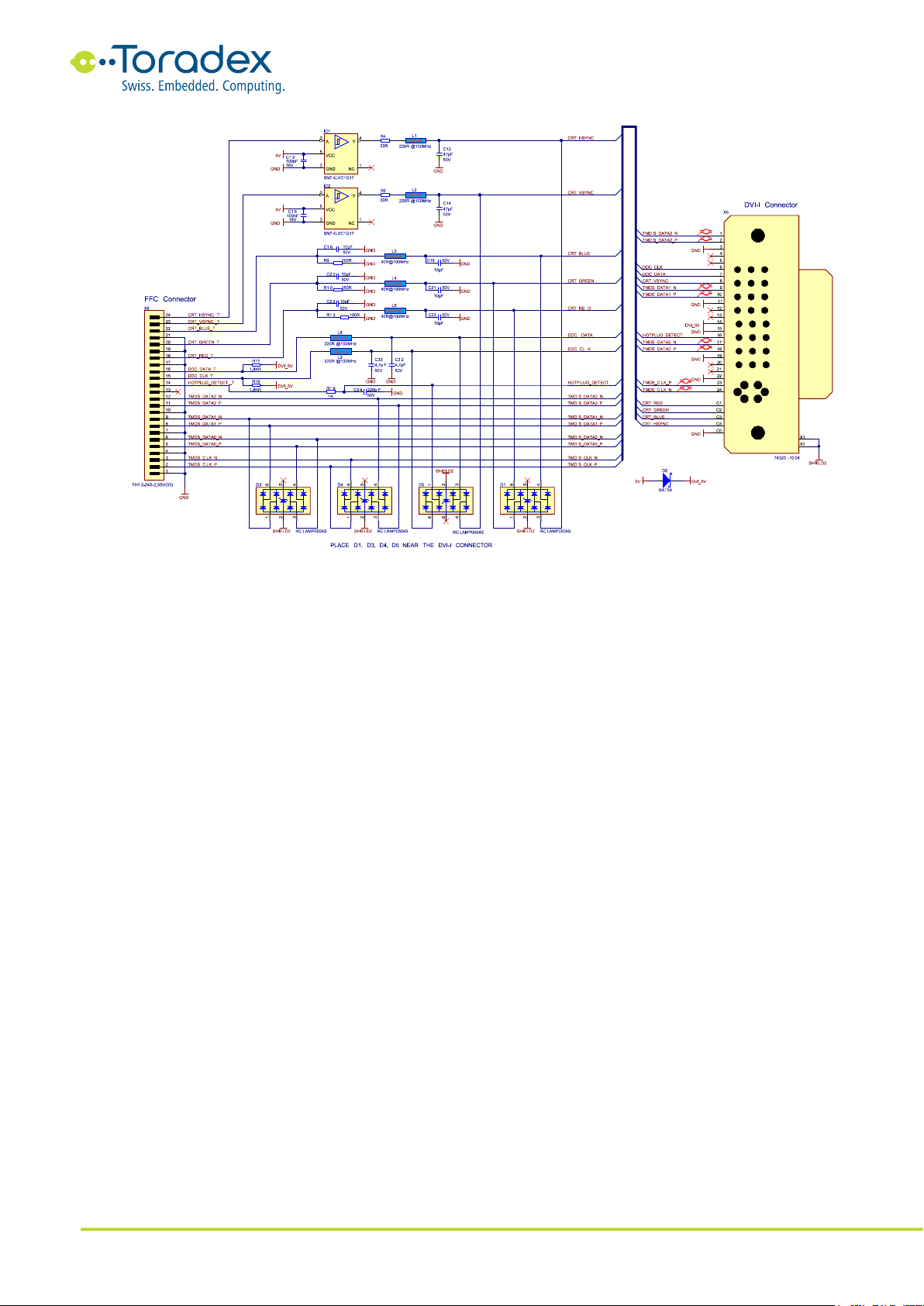
There are different configurations of DVI connectors available. The DVI-D (digital) contains only the
native DVI signals. The DVI-A (analog) provides no DVI signals. Only the analog VGA signals are
provided. The DVI-I (integrated) combines the digital DVI signals and the analog VGA signals. For
the DVI-A and DVI-I, there are passive adapters available for the D-SUB VGA connector. There is
only one DDC channel available on the DVI-I interface. Therefore, the connector is not designed to
use both links (DVI and VGA) contemporaneously. Nevertheless, there are Y-cables available that
provide a DVI and VGA output contemporaneously. Such cables are not standardized and usually
provide the DDC only on the DVI or VGA output. Please be aware of the DDC when using such a
Y-cable.
The following schematic example shows a DVI-I implementation. It can also be used as an example
for a DVI-D design. Just remove the analog VGA signals. The sync signals for the VGA signals need
to be level shifted from 3.3V to 5V. The same is necessary for the DDC signals. The TDMS signals
need to be ESD protected by using diodes. The schematic example shows a discrete solution for the
level shifting and protection. There are also integrated solutions available.
Colibri Carrier Board Design Guide
Toradex AG l Altsagenstrasse 5 l 6048 Horw l Switzerland l +41 41 500 48 00 l www.toradex.com l info@toradex.com
Page | 20
Figure 12: DVI-I Reference Schematic
2.5.2.2 HDMI Schematic Example
The HDMI connector does not feature an Analog VGA interface, but an optional Consumer
Electronics Control (CEC) interface is available on the connector. The location of the CEC signal is
not standardized on the Colibri modules. Check the datasheet of the modules for more
information on the position of the signal. The CEC is a single-wire interface used to control
consumer audio and video devices such as television sets or AV receivers. There are many different
CEC trade names (VIERA Link, Anynet+, EasyLink, Aquos Link, BRAVIA Link, and others.). The CEC
is a 3.3V interface. Nevertheless, it is recommended to add a level shifter from the internal 3.3V
logic level. This eliminates problems with displays that pull-up the signal to other voltage levels.
The I2C signals for the DDC and the hotplug detection (HPD) need to be shifted to/from the 5V
logic level of the HDMI to the Colibri level of 3.3V. The HPD has a 100kΩpull-down resistor
already on the baseboard
Table of contents
Other Toradex Carrier Board manuals


