Acromag VPX4812 User manual

Artisan Technology Group is your source for quality
new and certied-used/pre-owned equipment
• FAST SHIPPING AND
DELIVERY
• TENS OF THOUSANDS OF
IN-STOCK ITEMS
• EQUIPMENT DEMOS
• HUNDREDS OF
MANUFACTURERS
SUPPORTED
• LEASING/MONTHLY
RENTALS
• ITAR CERTIFIED
SECURE ASSET SOLUTIONS
SERVICE CENTER REPAIRS
Experienced engineers and technicians on staff
at our full-service, in-house repair center
WE BUY USED EQUIPMENT
Sell your excess, underutilized, and idle used equipment
We also offer credit for buy-backs and trade-ins
www.artisantg.com/WeBuyEquipment
REMOTE INSPECTION
Remotely inspect equipment before purchasing with
our interactive website at www.instraview.com
LOOKING FOR MORE INFORMATION?
Visit us on the web at www.artisantg.com for more
information on price quotations, drivers, technical
specications, manuals, and documentation
Contact us: (888) 88-SOURCE | sales@artisantg.com | www.artisantg.com
SM
View
Instra

VPX4812/4814
Single-Slot 3U VPX Bus
XMC Carrier Card with P16 Support
VPX Switch Card
USER’S MANUAL
ACROMAG INCORPORATED
30765 South Wixom Road
Wixom, MI 48393-2417 U.S.A.
Tel: (248) 295-0310
Copyright 2019, Acromag, Inc., Printed in the USA.
Data and specifications are subject to change without notice.
8501022D

VPX4812/4814 User’s Manual Single-Slot 3U VPX Bus XMC Carrier Card/Switch Card Module
Acromag, Inc. Tel: 248-295-0310 -
2
- www.acromag.com
The information contained in this manual is subject to change without notice. Acromag, Inc. makes no
warranty of any kind with regard to this material, including, but not limited to, the implied warranties of
merchantability and fitness for a particular purpose. Further, Acromag, Inc. assumes no responsibility
for any errors that may appear in this manual and makes no commitment to update, or keep current,
the information contained in this manual.
No part of this manual may be copied or reproduced in any form, without the prior written consent of
Acromag, Inc.
IMPORTANT SAFETY CONSIDERATIONS
It is very important for the user to consider the possible adverse effects of power, wiring, component,
sensor, or software failures in designing any type of control or monitoring system. This is especially
important where economic property loss or human life is involved. It is important that the user
employ satisfactory overall system design. It is agreed between the Buyer and Acromag, that this is
the Buyer's responsibility.

VPX4812/4814 User’s Manual Single-Slot 3U VPX Bus XMC Carrier Card/Switch Card Module
Acromag, Inc. Tel: 248-295-0310 -
3
- www.acromag.com
1.0 General Information ........................................................................................................................5
Key Features.....................................................................................................................................5
Introduction .....................................................................................................................................6
Module and Backplane Profiles .......................................................................................................6
Build Levels ......................................................................................................................................7
2.0 Ordering Information.......................................................................................................................8
3.0 Preparation For Use.........................................................................................................................9
Unpacking and Inspection................................................................................................................9
4.0 Operational Block Diagram............................................................................................................10
5.0 Board Layout..................................................................................................................................11
6.0 Connectors.....................................................................................................................................12
P0 Connector .................................................................................................................................12
P1 Connector .................................................................................................................................12
P2 Connector .................................................................................................................................13
J15 Connector ................................................................................................................................13
J16 Connector ................................................................................................................................14
J5 Connector –JTAG Header..........................................................................................................14
7.0 Switch Settings...............................................................................................................................15
Front Panel Layout.........................................................................................................................17
8.0 Handling.........................................................................................................................................18
ESD Safe Work Area Guidelines .....................................................................................................18
9.0 Installation .....................................................................................................................................19
Board Keying ..................................................................................................................................19
Installation Notes...........................................................................................................................19
10.0 Specifications .................................................................................................................................20
Physical ..........................................................................................................................................20
Front Panel.....................................................................................................................................20
Power Requirements .....................................................................................................................20
Power Consumption ......................................................................................................................20
Auxiliary Supply..............................................................................................................................21
Power-Up/Reset Sequence............................................................................................................21
Bus Compliance..............................................................................................................................21
Form Factor....................................................................................................................................21
Flammability ..................................................................................................................................21
Environmental................................................................................................................................22

VPX4812/4814 User’s Manual Single-Slot 3U VPX Bus XMC Carrier Card/Switch Card Module
Acromag, Inc. Tel: 248-295-0310 -
4
- www.acromag.com
EMI/EMC Regulatory Compliance..................................................................................................23
11.0 Service and Repair .........................................................................................................................24
Service and Repair Assistance........................................................................................................24
Preliminary Service Procedure.......................................................................................................24
Where to Get Help.........................................................................................................................24
Appendix A –Accessory Modules...............................................................................................................25
TRANS-V112...................................................................................................................................25
Certificate of Volatility ................................................................................................................................29
Revision History ..........................................................................................................................................30

VPX4812/4814 User’s Manual Single-Slot 3U VPX Bus XMC Carrier Card/Switch Card Module
Acromag, Inc. Tel: 248-295-0310 -
5
- www.acromag.com
1.0 General Information
The VPX4812 is an XMC Carrier Card Module in the 3U VPX form factor, targeted for processing,
communications, and display applications in the commercial, military, and aerospace markets.
The VPX4812 provides support for Rear I/O connections from the XMC P16 connector. The
TRANS-V112 is the Rear Transition Module for the VPX4812 used to bring out Rear I/O
connections through the backplane.
The VPX4812 supports up to four VPX Fat Pipe (x4) connections to other cards in the system at
Gen 2.0 speeds. The VPX4812 can be used as a switch card allowing an upstream Fat Pipe or
Double Fan Pipe connection –typically to a CPU –to communicate with up to three downstream
Fat Pipe connections or a single Double Fat Pipe connection.
The VPX4812 also provides support for a VPX Double Fat Pipe (x8) connection to an XMC card at
Gen 2.0 speeds.
The VPX4814 disconnects the PCIe connection to the third downstream card allowing it to be
used in systems with an Ethernet control plane interface. This provides the VPX4814 with the
ability to be used as an XMC Carrier Card in the majority of the standard OpenVPX profiles.
Key Features
•24-Channel 5-Port PCI Express Gen. 2.0 Switch
•The XMC site is PCIe 8-Lanes Gen. 2.0
•Module conforms to VPX Spec. VITA 46.0, 46.4, and 46.9
•The XMC site supports X24s+X8d+X12d I/O mapping (VITA
46.9)
•16 Lanes PCI Express to backplane (VITA 46.0 and 46.4)
•Supports Non-Transparent Bridging Applications
•3U VPX form factor supporting OpenVPX/VITA 65
•Air and conduction cooled variants available
•REDI covers supporting VITA 48 available
VPX4812/4814 User’s Manual Single-Slot 3U VPX Bus XMC Carrier Card/Switch Card Module
Acromag, Inc. Tel: 248-295-0310 -
6
- www.acromag.com
Introduction
The VPX4812 has two primary functions that can be utilized in a VPX system simultaneously.
1. XMC Carrier Card –The VPX4812 supports a Double Fat Pipe (x8) connection from an
XMC module to the on-board PCIe switch. The voltage used to power the XMC module
can be toggled between 5V or 12V using a DIP switch located on the VPX4812.
2. VPX Switch Card –The VPX4812 contains a 24-lane 5-port PCIe switch capable of Gen
2.0 speeds. When utilizing the VPX4812 as a switch card, a CPU module configured to be
an upstream port can communicate with up to three downstream VPX cards in the
system as well as an XMC module on the 4812.
The VPX4812 supports the use of non-transparent bridging using the on-board PCIe switch. By
utilizing non-transparent bridging (NTB), the VPX4812 can be used to implement multi-hosted
topologies including intelligent adapter cards, dual-host systems with redundancy, and even
blade server systems.
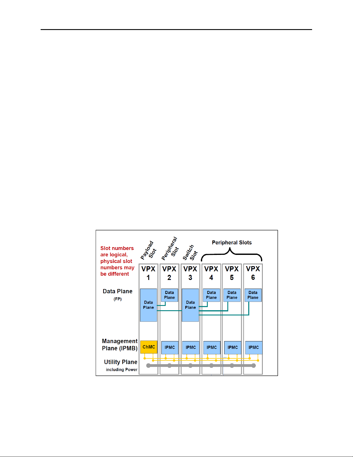
Module and Backplane Profiles
The VPX4812 conforms to OpenVPX switch module profile MOD3-SWH-4F-16.4.5-2. This switch
profile is intended to be used in the OpenVPX backplane profile BKP3-CEN06-15.2.12-n shown
below.
Figure 1: OpenVPX Backplane Profile BKP3-CEN06-15.2.12-n

VPX4812/4814 User’s Manual Single-Slot 3U VPX Bus XMC Carrier Card/Switch Card Module
Acromag, Inc. Tel: 248-295-0310 -
7
- www.acromag.com
The VPX4812 also conforms to OpenVPX peripheral module profile MOD3-PER-1F-14.3.2 when
used as an XMC carrier card. Typically, this peripheral profile can be used in a wide range of
OpenVPX backplane profiles but due to the PCIe switch connections on P1, the VPX4812 may be
incompatible with profiles that contain other plane interfaces on P1. Check the VPX connector
pinout in this manual against the intended backplane topology to ensure compatibility.
The VPX4814 disconnects the lower PCIe lanes on P1 while retaining all of the XMC carrier card
functionality of the VPX4812. This allows it to be used as an XMC carrier card in a wider range of
OpenVPX backplane profiles including profiles that contain Ethernet control plane interfaces on
P1.
Build Levels
The VPX4812/14 is available in three electrically compatible build levels, each of which is
carefully tailored to a particular set of requirements and environments. All three levels fully
support the power and versatility of VPX, so no matter how large or diversified your project,
absolute compatibility is assured at all stages of development. The three build levels have three
basic mechanical configurations, both in accordance with the VITA 46.0 VPX standard and the
VITA 48 REDI standard:
1. Air (convection) cooled modules are intended for use in standard industrial chassis.
2. Conduction-cooled modules are intended for use in sealed Air Transportable Racking
(ATR) and other conduction-cooled environments.
3. REDI cover, Conduction-cooled modules are intended for use in sealed Air Transportable
Racking (ATR) and other conduction-cooled environments.

VPX4812/4814 User’s Manual Single-Slot 3U VPX Bus XMC Carrier Card/Switch Card Module
Acromag, Inc. Tel: 248-295-0310 -
8
- www.acromag.com
2.0 Ordering Information
Available Models
VPX4812-LF
VPX4812 Air-cooled Model
VPX4812-CC-LF
VPX4812 Conduction-cooled Model
VPX4812-REDI-LF
VPX4812 REDI Model
VPX4814-LF
VPX4814 Air-cooled Model
VPX4814-CC-LF
VPX4814 Conduction-cooled Model
VPX4814-REDI-LF
VPX4814 REDI Model
VPX4812/4814 User’s Manual Single-Slot 3U VPX Bus XMC Carrier Card/Switch Card Module
Acromag, Inc. Tel: 248-295-0310 -
9
- www.acromag.com
3.0 Preparation For Use
Unpacking and Inspection
Upon receipt of this product, inspect the shipping carton for evidence
of mishandling during transit. If the shipping carton is badly
damaged or water stained, request that the carrier's agent be present
when the carton is opened.
If the carrier's agent is absent when the carton is opened, and the
contents of the carton are damaged, keep the carton and packing
material for the agent's inspection.
For repairs to a product damaged in shipment, refer to the Acromag
Service Policy to obtain return instructions. It is suggested that
salvageable shipping cartons and packing material be saved for future
use in the event the product must be shipped.
This board is physically protected with packing material and
electrically protected with an anti-static bag during shipment. It is
recommended that the board be visually inspected for evidence of
mishandling prior to applying power.
The board utilizes static sensitive components and should only be
handled at a static-safe workstation.
IMPORTANT: Adequate air circulation must be provided to prevent a temperature rise above the
maximum operating temperature.
Adequate air circulation must be provided to prevent a temperature rise above the maximum
operating temperature and to prolong the life of the electronics.
If the installation is in an industrial environment and the board is exposed to environmental air,
careful consideration should be given to air-filtering.

VPX4812/4814 User’s Manual Single-Slot 3U VPX Bus XMC Carrier Card/Switch Card Module
Acromag, Inc. Tel: 248-295-0310 -
10
- www.acromag.com
4.0 Operational Block Diagram

VPX4812/4814 User’s Manual Single-Slot 3U VPX Bus XMC Carrier Card/Switch Card Module
Acromag, Inc. Tel: 248-295-0310 -
11
- www.acromag.com
5.0 Board Layout
VPX4812/4814 User’s Manual Single-Slot 3U VPX Bus XMC Carrier Card/Switch Card Module
Acromag, Inc. Tel: 248-295-0310 -
12
- www.acromag.com
6.0 Connectors
P0 Connector
P0 Wafer
A
B
C
D
E
F
G
1
+3.3 V
+3.3 V
+3.3 V
Unused
+12 V
+12 V
+12 V
2
+3.3 V
+3.3 V
+3.3 V
Unused
+12 V
+12 V
+12 V
3
+5 V
+5 V
+5 V
Unused
+5 V
+5 V
+5 V
4
NVRAM_LOCK
PLT_RST#
GND
-12V_AUX
GND
Unused
Unused
5
SMB_DATA
SMB_CLK
GND
+3.3V AUX
GND
Unused
Unused
6
GA0#
GA1#
GND
+12V_AUX
GND
GA2#
GA3#
7
Unused
Unused
GND
Unused
Unused
GND
Unused
8
GND
Unused
Unused
GND
PCIe VPX
REF_CLK P
PCIe VPX
REF_CLK N
GND
# = Low true signal
P1 Connector
P1 Wafer
A
B
C
D
E
F
G
1
PCIE_VPX_P0_RXP
PCIE_VPX_P0_RXN
GND
PCIE_VPX_P0_TXP
PCIE_VPX_P0_TXN
GND
Unused
2
GND
PCIE_VPX_P1_RXP
PCIE_VPX_P1_RXN
GND
PCIE_VPX_P1_TXP
PCIE_VPX_P1_TXN
GND
3
PCIE_VPX_P2_RXP
PCIE_VPX_P2_RXN
GND
PCIE_VPX_P2_TXP
PCIE_VPX_P2_TXN
GND
Unused
4
GND
PCIE_VPX_P3_RXP
PCIE_VPX_P3_RXN
GND
PCIE_VPX_P3_TXP
PCIE_VPX_P3_TXN
GND
5
PCIE_VPX_P4_RXP
PCIE_VPX_P4_RXN
GND
PCIE_VPX_P4_TXP
PCIE_VPX_P4_TXN
GND
Unused
6
GND
PCIE_VPX_P5_RXP
PCIE_VPX_P5_RXN
GND
PCIE_VPX_P5_TXP
PCIE_VPX_P5_TXN
GND
7
PCIE_VPX_P6_RXP
PCIE_VPX_P6_RXN
GND
PCIE_VPX_P6_TXP
PCIE_VPX_P6_TXN
GND
Unused
8
GND
PCIE_VPX_P7_RXP
PCIE_VPX_P7_RXN
GND
PCIE_VPX_P7_TXP
PCIE_VPX_P7_TXN
GND
9
PCIE_VPX_P8_RXP
PCIE_VPX_P8_RXN
GND
PCIE_VPX_P8_TXP
PCIE_VPX_P8_TXN
GND
Unused
10
GND
PCIE_VPX_P9_RXP
PCIE_VPX_P9_RXN
GND
PCIE_VPX_P9_TXP
PCIE_VPX_P9_TXN
GND
11
PCIE_VPX_P10_RXP
PCIE_VPX_P10_RXN
GND
PCIE_VPX_P10_TXP
PCIE_VPX_P10_TXN
GND
Unused
12
GND
PCIE_VPX_P11_RXP
PCIE_VPX_P11_RXN
GND
PCIE_VPX_P11_TXP
PCIE_VPX_P11_TXN
GND
13
PCIE_VPX_P12_RXP1
PCIE_VPX_P12_RXN1
GND
PCIE_VPX_P12_TXP1
PCIE_VPX_P12_TXN1
GND
Unused
14
GND
PCIE_VPX_P13_RXP1
PCIE_VPX_P13_RXN1
GND
PCIE_VPX_P13_TXP1
PCIE_VPX_P13_TXN1
GND
15
PCIE_VPX_P14_RXP1
PCIE_VPX_P14_RXN1
GND
PCIE_VPX_P14_TXP1
PCIE_VPX_P14_TXN1
GND
Unused
16
GND
PCIE_VPX_P15_RXP1
PCIE_VPX_P15_RXN1
GND
PCIE_VPX_P15_TXP1
PCIE_VPX_P15_TXN1
GND
Note 1: These signals are unconnected on all VPX4814 models.
RX is defined as a signal that is an input to the VPX4812.
TX is defined as a signal that is an output from the VPX4812.

VPX4812/4814 User’s Manual Single-Slot 3U VPX Bus XMC Carrier Card/Switch Card Module
Acromag, Inc. Tel: 248-295-0310 -
13
- www.acromag.com
P2 Connector
P2 Wafer
A
B
C
D
E
F
G
1
J16_SIO11_P
J16_SIO11_N
GND
J16_SIO10_P
J16_SIO10_N
GND
Unused
2
GND
J16_SIO9_P
J16_SIO9_N
GND
J16_SIO8_P
J16_SIO8_N
GND
3
J16_SIO7_P
J16_SIO7_N
GND
J16_SIO6_P
J16_SIO6_N
GND
Unused
4
GND
J16_SIO5_P
J16_SIO5_N
GND
J16_SIO4_P
J16_SIO4_N
GND
5
J16_SIO3_P
J16_SIO3_N
GND
J16_SIO2_P
J16_SIO2_N
GND
Unused
6
GND
J16_SIO1_P
J16_SIO1_N
GND
J16_SIO0_P
J16_SIO0_N
GND
7
J16_DP01_N
J16_DP01_P
GND
J16_DP00_N
J16_DP00_P
GND
Unused
8
GND
J16_DP03_N
J16_DP03_P
GND
J16_DP02_N
J16_DP02_P
GND
9
J16_DP11_N
J16_DP11_P
GND
J16_DP10_N
J16_DP10_P
GND
Unused
10
GND
J16_DP13_N
J16_DP13_P
GND
J16_DP12_N
J16_DP12_P
GND
11
J16_DP05_N
J16_DP05_P
GND
J16_DP04_N
J16_DP04_P
GND
Unused
12
GND
J16_DP07_N
J16_DP07_P
GND
J16_DP06_N
J16_DP06_P
GND
13
J16_DP09_N
J16_DP09_P
GND
J16_DP08_N
J16_DP08_P
GND
Unused
14
GND
J16_DP15_N
J16_DP15_P
GND
J16_DP14_N
J16_DP14_P
GND
15
J16_DP17_N
J16_DP17_P
GND
J16_DP16_N
J16_DP16_P
GND
Unused
16
GND
J16_DP19_N
J16_DP19_P
GND
J16_DP18_N
J16_DP18_P
GND
J15 Connector
A
B
C
D
E
F
1
PCIE_XMC_P0_RXP
PCIE_XMC_P0_RXN
+3.3V
PCIE_XMC_P1_RXP
PCIE_XMC_P1_RXN
VPWR
2
GND
GND
NC
GND
GND
XMC_RSTI#
3
PCIE_XMC_P2_RXP
PCIE_XMC_P2_RXN
+3.3V
PCIE_XMC_P3_RXP
PCIE_XMC_P3_RXN
VPWR
4
GND
GND
JTAG_TCK
GND
GND
XMC_RSTO#
5
PCIE_XMC_P4_RXP
PCIE_XMC_P4_RXN
+3.3V
PCIE_XMC_P5_RXP
PCIE_XMC_P5_RXN
VPWR
6
GND
GND
JTAG_TMS
GND
GND
+12V
7
PCIE_XMC_P6_RXP
PCIE_XMC_P6_RXN
+3.3V
PCIE_XMC_P7_RXP
PCIE_XMC_P7_RXN
VPWR
8
GND
GND
JTAG_TDI
GND
GND
-12V_AUX
9
NC
NC
NC
NC
NC
VPWR
10
GND
GND
JTAG_TDO
GND
GND
GA0#
11
PCIE_XMC_P0_TXP
PCIE_XMC_P0_TXN
NC
PCIE_XMC_P1_TXP
PCIE_XMC_P1_TXN
VPWR
12
GND
GND
GA1#
GND
GND
NC
13
PCIE_XMC_P2_TXP
PCIE_XMC_P2_TXN
+3.3V_AUX
PCIE_XMC_P3_TXP
PCIE_XMC_P3_TXN
VPWR
14
GND
GND
GA2#
GND
GND
SMB_DATA
15
PCIE_XMC_P4_TXP
PCIE_XMC_P4_TXN
NC
PCIE_XMC_P5_TXP
PCIE_XMC_P5_TXN
VPWR
16
GND
GND
NVRAM_LOCK
GND
GND
SMB_CLK
17
PCIE_XMC_P6_TXP
PCIE_XMC_P6_TXN
NC
PCIE_XMC_P7_TXP
PCIE_XMC_P7_TXN
NC
18
GND
GND
NC
GND
GND
NC
19
PCIE_VPX REF_CLK P
PCIE_VPX REF_CLK N
NC
NC
ROOT0#
NC
# = Low true signal

VPX4812/4814 User’s Manual Single-Slot 3U VPX Bus XMC Carrier Card/Switch Card Module
Acromag, Inc. Tel: 248-295-0310 -
14
- www.acromag.com
J16 Connector
A
B
C
D
E
F
1
J16_DP00_P
J16_DP00_N
NC
J16_DP01_P
J16_DP01_N
NC
2
GND
GND
NC
GND
GND
NC
3
J16_DP02_P
J16_DP02_N
NC
J16_DP03_P
J16_DP03_N
NC
4
GND
GND
NC
GND
GND
NC
5
J16_DP04_P
J16_DP04_N
NC
J16_DP05_P
J16_DP05_N
NC
6
GND
GND
NC
GND
GND
NC
7
J16_DP06_P
J16_DP06_N
NC
J16_DP07_P
J16_DP07_N
NC
8
GND
GND
J16_SIO10_N
GND
GND
J16_SIO11_N
9
J16_DP08_P
J16_DP08_N
J16_SIO10_P
J16_DP09_P
J16_DP09_N
J16_SIO11_P
10
GND
GND
J16_SIO8_N
GND
GND
J16_SIO9_N
11
J16_DP10_P
J16_DP10_N
J16_SIO8_P
J16_DP11_P
J16_DP11_N
J16_SIO9_P
12
GND
GND
J16_SIO6_N
GND
GND
J16_SIO7_N
13
J16_DP12_P
J16_DP12_N
J16_SIO6_P
J16_DP13_P
J16_DP13_N
J16_SIO7_P
14
GND
GND
J16_SIO4_N
GND
GND
J16_SIO5_N
15
J16_DP14_P
J16_DP14_N
J16_SIO4_P
J16_DP15_P
J16_DP15_N
J16_SIO5_P
16
GND
GND
J16_SIO2_N
GND
GND
J16_SIO3_N
17
J16_DP16_P
J16_DP16_N
J16_SIO2_P
J16_DP17_P
J16_DP17_N
J16_SIO3_P
18
GND
GND
J16_SIO0_N
GND
GND
J16_SIO1_N
19
J16_DP18_P
J16_DP18_N
J16_SIO0_P
J16_DP19_P
J16_DP19_N
J16_SIO1_P
J5 Connector –JTAG Header
Pin Number
Description
1
JTAG_TDI
2
JTAG_TDO
3
GND
4
JTAG_TCK
5
JTAG_TMS
6
JTAG_VREF

VPX4812/4814 User’s Manual Single-Slot 3U VPX Bus XMC Carrier Card/Switch Card Module
Acromag, Inc. Tel: 248-295-0310 -
15
- www.acromag.com
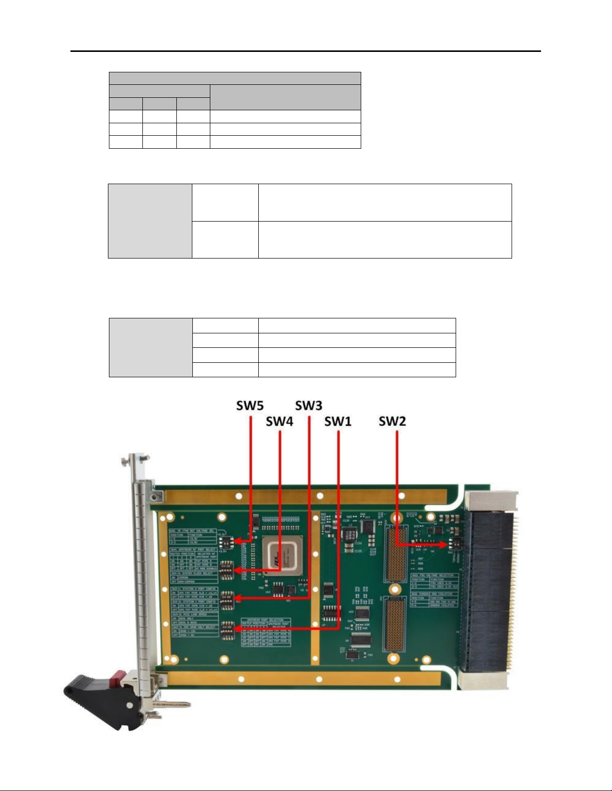
7.0 Switch Settings
The following describes the VPX4812 switches with their default positions and their functions.
SW1 –Upstream Port Selection
Switch Position
Selected Upstream Port
1
2
3
4
ON
ON
ON
ON
VPX Fat Pipe A (default)
OFF
ON
ON
ON
VPX Fat Pipe B
OFF
ON
OFF
ON
VPX Fat Pipe C
ON
OFF
OFF
ON
VPX Fat Pipe D
ON
ON
ON
OFF
XMC
SW2
(FRUSEL &
ORBGND)
1-2 (default)
FRU uses 3.3V
2-3
FRU uses 3.3V_AUX
4-5 (default)
Orb ground is connected to digital ground.
5-6
Orb ground is isolated from digital ground.
Orb ground is the front panel and the VPX key-guides.
SW3-1
(STATION 0 PORT
CONFIG)
ON (default)
VPX Fat Pipe A = x4, VPX Fat Pipe B = x4
OFF
VPX Fat Pipe A = x8, VPX Fat Pipe B = Disabled
SW3-2
(STATION 1 PORT
CONFIG)
ON
VPX Fat Pipe C = x8, VPX Fat Pipe D = Disabled
OFF (default)
VPX Fat Pipe C = x4, VPX Fat Pipe D = x4
SW3-3
(PCIE LINK
SPEED)
ON
Force Gen 1.0 Speed Only
OFF (default)
Allow Gen 1.0 & Gen 2.0 Speeds
SW3-4
(XMC VPWR
VOLT SELECT)
ON
VPWR = +12V
OFF (default)
VPWR = +5V
VPX4812/4814 User’s Manual Single-Slot 3U VPX Bus XMC Carrier Card/Switch Card Module
Acromag, Inc. Tel: 248-295-0310 -
16
- www.acromag.com
SW4-1:3 –Upstream NT Port Selection
Switch Position
Selected NT Upstream Port
1
2
3
ON
ON
ON
VPX Fat Pipe A
ON
OFF
ON
VPX Fat Pipe B
OFF
OFF
OFF
NT Mode Disabled (default)
Note: In addition to the switch configuration, there are settings for the PEX8624 that must be programmed to the on-
board EEPROM device to enable Non-Transparent Mode.
SW4-4
(SYSTEM CLOCK
SELECT)
ON
(Common) Uses the 100MHz reference clock pins on the
VPX bus generated by the CPU board for PCIe timing. (Pins
E8 & F8 on the VPX P0 connector)
OFF (default)
(Non-Common) Uses the 100MHz reference clock
generated on board for PCIe timing.
Note: Best system stability may be achieved with the use of a 100MHz common clock connection from the SBC,
especially at Gen 2.0 link speeds. If the system does not provide a common clock, then non-common clock mode must
be used.
SW5
(JTAG VREF
SELECT)
1-2 (default)
JTAG_VREF = +3.3V
2-3
JTAG_VREF = +2.5V
4-5
Unused
5-6
Unused

VPX4812/4814 User’s Manual Single-Slot 3U VPX Bus XMC Carrier Card/Switch Card Module
Acromag, Inc. Tel: 248-295-0310 -
17
- www.acromag.com
Front Panel Layout
VPX4812 Front Panel
On the front panel of air-cooled VPX4812 assemblies, there are 5 port status LED’s. The first four
LED’s indicate the PCIe link status for each of the four Fat Pipe connections to other slots on the
VPX backplane. The fifth LED on the front panel indicates the PCIe link status of an XMC module
connected to the VPX4812. The table below describes what the LED On/Off patterns indicate
about the corresponding port states.
Port Status LED On/Off Patterns, by State
State
LED Pattern
Link is down
Off
Link is up, Gen 2.0 speed, all Lanes are up
On
Link is up, Gen 2.0 speed, reduced Lanes are up
Blinking, 0.5 seconds On, 0.5 seconds Off
Link is up, Gen 1.0 speed, all Lanes are up
Blinking, 1.5 seconds On, 0.5 seconds Off
Link is up, Gen 1.0 speed, reduced Lanes are up
Blinking, 0.5 seconds On, 1.5 seconds Off

VPX4812/4814 User’s Manual Single-Slot 3U VPX Bus XMC Carrier Card/Switch Card Module
Acromag, Inc. Tel: 248-295-0310 -
18
- www.acromag.com
8.0 Handling
Modules should be handled in ESD-safe work areas in order to
prevent damage to sensitive components from electrostatic
discharges. These areas must be designed and maintained to prevent
ESD damage.
ESD Safe Work Area Guidelines
1. Module should be handled at properly designated work areas
only.
2. Designated ESD safe work areas must be checked periodically to
ensure their continued safety from ESD. The areas should be
monitored for the following:
a. Proper grounding methods.
b. Static dissipation of work surfaces.
c. Static dissipation of floor surfaces.
d. Operation of ion blowers and ion air guns.
3. Designated work areas must be kept free of static generating
materials such as Styrofoam, vinyl, plastic, fabrics, or any other
static generating materials.
4. Work areas must be kept clean and neat in order to prevent
contamination of the work area.
5. Modules should be handled by the edges. Avoid touching
component leads.
NOTE: When not installed in a system, modules must be enclosed
in shielded bags or boxes. There are three types of ESD protective
enclosure materials this module was shipped in an approved ESD
bag.
6. Whenever handling the module, the operator must be properly
grounded by one of the following:
a. Wearing a wrist strap connected to earth ground.
b. Wearing heel grounders and have both feet on a static
dissipative floor surface.
7. Stacking of modules should be avoided to prevent physical
damage.

VPX4812/4814 User’s Manual Single-Slot 3U VPX Bus XMC Carrier Card/Switch Card Module
Acromag, Inc. Tel: 248-295-0310 -
19
- www.acromag.com
9.0 Installation
IMPORTANT: The VPX4812 has been specifically design for use with 3U VPX backplanes and my not be
compatible with some 6U backplanes. Plugging the board into an unsupported 6U VPX backplane may
cause permanent damage.
Consult the enclosure documentation to ensure that the VPX4812’s power requirements are compatible
with those supplied by the backplane.
Board Keying
The 3U VPX backplane specification requires all backplane slots
to have two guide pins: one above the J0 connector and one
below the J2 connector. As well as providing correct alignment,
these pins are keyed to prevent cards from being inserted into
incorrect backplane slot(s) to avoid electrical incompatibility.
The VPX4812 has receptacles for these guide pins (see the
Connectors section). By default, these are not keyed. Please
contact the factory to discuss keying requirements.
Installation Notes
1. Keying may dictate the backplane slot(s) into which the
VPX4812 can be inserted.
2. Air-cooled versions have an ejector handle to ensure that
the backplane connectors mate properly with the
backplane. The captive screws at the top and bottom of the
front panel allow the VPX4812 to be tightly secured in
position, which provides continuity with system chassis
ground.
3. Conduction-cooled and REDI versions have screw driven
wedge locks at the top and bottom of the board to provide
the necessary mechanical/thermal interface. Correct
adjustment requires a calibrated torque wrench set to
between 0.6 and 0.8 Nm.
This manual suits for next models
7
Table of contents
Other Acromag Carrier Board manuals

Acromag
Acromag APC8620 Series User manual

Acromag
Acromag VPX4812A User manual

Acromag
Acromag AVME9675 Series User manual

Acromag
Acromag ACPC4610E/CC User manual

Acromag
Acromag XMCAP2022 User manual

Acromag
Acromag AVME9630 Series User manual

Acromag
Acromag AVME9675A Series User manual

Acromag
Acromag ACEX4041 User manual


