ETAS ES1651.1-B User manual

ES1651.1-B Carrier Board
User’s Guide

2
Copyright
The data in this document may not be altered or amended without special
notification from ETAS GmbH. ETAS GmbH undertakes no further obligation
in relation to this document. The software described in it can only be used if
the customer is in possession of a general license agreement or single license.
Using and copying is only allowed in concurrence with the specifications
stipulated in the contract.
Under no circumstances may any part of this document be copied, repro-
duced, transmitted, stored in a retrieval system or translated into another
language without the express written permission of ETAS GmbH.
© Copyright 2018 ETAS GmbH, Stuttgart
The names and designations used in this document are trademarks or brands
belonging to the respective owners.
V1.0.0 R04 EN - 07.2018

Contents 3
Contents
1Introduction . . . . . . . . . . . . . . . . . . . . . . . . . . . . . . . . . . . . . . . . . . . . . . . . . . . . . 5
1.1 Applications and Features . . . . . . . . . . . . . . . . . . . . . . . . . . . . . . . . . . . . . 6
1.2 Block Diagram . . . . . . . . . . . . . . . . . . . . . . . . . . . . . . . . . . . . . . . . . . . . . . 8
2Hardware Features . . . . . . . . . . . . . . . . . . . . . . . . . . . . . . . . . . . . . . . . . . . . . . . . 9
2.1 Carrier Board for Piggybacks . . . . . . . . . . . . . . . . . . . . . . . . . . . . . . . . . . . 9
2.2 Inspection and Versioning Data . . . . . . . . . . . . . . . . . . . . . . . . . . . . . . . . . 9
3Configuration. . . . . . . . . . . . . . . . . . . . . . . . . . . . . . . . . . . . . . . . . . . . . . . . . . . 11
3.1 Configuration of the Debug Port Connections of the Processor (JP0) . . . . 11
3.2 JTAG Chain Configuration (JP1) . . . . . . . . . . . . . . . . . . . . . . . . . . . . . . . . 12
3.3 Boot Configuration (SW0) . . . . . . . . . . . . . . . . . . . . . . . . . . . . . . . . . . . . 13
3.4 Reset Switch (SW3) . . . . . . . . . . . . . . . . . . . . . . . . . . . . . . . . . . . . . . . . . 13
3.5 Addressing the ES1651.1-B at the VMEbus (SW1 and SW2) . . . . . . . . . . 14
4Installing I/O Modules . . . . . . . . . . . . . . . . . . . . . . . . . . . . . . . . . . . . . . . . . . . . . 17
4.1 Assembling the Front Panel to the PB4350XXX Module . . . . . . . . . . . . . . 17
4.2 Mounting the I/O Modules . . . . . . . . . . . . . . . . . . . . . . . . . . . . . . . . . . . 20
5Pin Assignments and Display Elements . . . . . . . . . . . . . . . . . . . . . . . . . . . . . . . . 25
5.1 Box Headers for I/O Modules (CO7 - CO10) . . . . . . . . . . . . . . . . . . . . . . . 25
5.2 ETAS-Internal Service Connection (CO11) . . . . . . . . . . . . . . . . . . . . . . . . 26

Contents4
5.3 Interface for Logic Analyser (CO12) . . . . . . . . . . . . . . . . . . . . . . . . . . . . . 26
5.4 LEDs . . . . . . . . . . . . . . . . . . . . . . . . . . . . . . . . . . . . . . . . . . . . . . . . . . . . 27
6Technical Data . . . . . . . . . . . . . . . . . . . . . . . . . . . . . . . . . . . . . . . . . . . . . . . . . . 29
6.1 Fulfilled Standards and Norms . . . . . . . . . . . . . . . . . . . . . . . . . . . . . . . . . 30
7ETAS Contact Addresses. . . . . . . . . . . . . . . . . . . . . . . . . . . . . . . . . . . . . . . . . . . 31
Index . . . . . . . . . . . . . . . . . . . . . . . . . . . . . . . . . . . . . . . . . . . . . . . . . . . . . . . . . 33

Introduction 5
1 Introduction
This User’s Guide contains the description of the ES1651.1-B Carrier Board.
It consists of the following chapters:
• "Applications and Features" on page 6
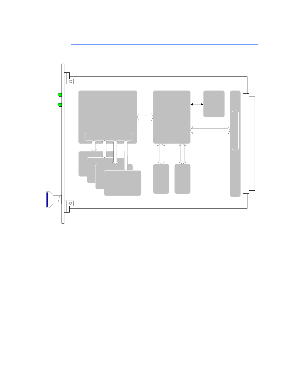
The introduction contains an overview of the characteristics of the
ES1651.1-B Carrier Board and also includes a block diagram.
• "Hardware Features" on page 9
This is where the properties of the ES1651.1-B Carrier Board are
described in detail. These are:
– "Carrier Board for Piggybacks" on page 9
– "Inspection and Versioning Data" on page 9
• "Configuration" on page 11
This section contains a description of the configuration possibilities of
the ES1651.1-B Carrier Board and their presettings.
• "Installing I/O Modules" on page 17
This section describes how to assemble I/O modules on the ES1651.1-
B Carrier Board and any necessary preparatory steps:
– "Assembling the Front Panel to the PB4350XXX Module"
on page 17
– "Mounting the I/O Modules" on page 20
• "Pin Assignments and Display Elements" on page 25
This section contains a description of all connectors on the front panel
and on the board as well as the meaning of the LED displays.
• "Technical Data" on page 29
contains the technical data of the ES1651.1-B Carrier Board.
Note
Some components of the ES1651.1-B Carrier Board may be damaged or
destroyed by electrostatic discharges. Please keep the board in its storage
package until it is installed.
The ES1651.1-B Carrier Board should only be taken from its package, con-
figured and installed at a working place that is protected against static dis-
charge.

Introduction6
1.1 Applications and Features
The ES1651.1-B Carrier Board acts as a carrier board for up to four I/O modules
in VMEbus systems. All modules of types ”PB4350XXX” and ”PB1651XXX”
can be used in any combination. An SPI control unit realized in the FPGA of the
board converts the parallel data flow of the processor into a serial bit flow for
the SPI interfaces of the I/O modules.
VMEbus Interface
The ES1651.1-B Carrier Board has a VMEbus slave interface and reacts to
”A24 non privileged data access” accesses (VMEbus address modifier 39 hex).
The position of the 64-kByte VMEbus address space of the board can be set
either dynamically or statically. Data is exchanged with VMEbus master boards
via a 32-kByte DPRAM. The board can trigger interrupts at the VMEbus.
Inspection and Versioning Data
Inspection and versioning data of the board are stored in a serial non-volatile
data memory.
Processor
The MPC555 processor of the board has a 448-kByte ROM memory which is
large enough for program code and data; this is why the optional external
ROM memory is not assembled.
Note
The components, connectors and conductors of the ES1651.1-B Carrier
Board may carry dangerous voltages.
These voltages may even exist when the board is not installed in the VMEbus
system or the VMEbus system is powered off.
Make sure that the board is protected against contact during operation.
Disconnect all connections to the ES1651.1-B Carrier Board before removing
the board from the VMEbus system.

Introduction8
1.2 Block Diagram
Fig. 1-2 shows a block diagram with all important functional units of the
ES1651.1-B Carrier Board.
Fig. 1-2 Block Diagram of the ES1651.1-B Carrier Board
FPGA Processor
Serial
ROM
External
RAM
(512
kByte)
External
ROM
(opt.)
32
VMEbus Interface
16
DPRAM (32 kByte)
16
I/O Module 3
SPI Control Unit
I/O Module 2
I/O Module 1
I/O Module 0
32

Hardware Features 9
2 Hardware Features
This section contains a description of the different hardware features of the
ES1651.1-B Carrier Board.
2.1 Carrier Board for Piggybacks
The ES1651.1-B Carrier Board is used as a carrier board for I/O modules in
VMEbus systems. I/O modules are available for various tasks, such as the gen-
eration and measuring of ECU signals in real time.
All modules of types ”PB4350XXX” and ”PB1651XXX” can be used. This
means that the LABCAR test system can be equipped both with the standard
I/O modules for the ES1651.1-B Carrier Board (VME system) and with the
highly precise I/O modules for the ES4350 Carrier Board. Up to four I/O mod-
ules of both types mentioned above can be used per ES1651.1-B Carrier
Board.
The I/O modules are connected using ribbon cable. There are four connectors
on the ES1651.1-B Carrier Board for this purpose. For more details on how to
assemble I/O modules, please refer to section
2.2 Inspection and Versioning Data
Inspection and versioning data of the board are stored in a serial non-volatile
data memory which is addressed via the processor’s SPI (Serial Peripheral Inter-
face). The data can be read out via the operating software LABCAR-OPERA-
TOR.

Hardware Features10

Configuration 11
3 Configuration
Fig. 3-1 shows the position of all connectors and switches for configuring the
ES1651.1-B Carrier Board - in addition to important components and connec-
tors for orientation purposes.
Fig. 3-1 Position of the Connectors, Jumpers and Switches (Component
Side)
3.1 Configuration of the Debug Port Connections of the Processor (JP0)
Tab. 3-1 JP0 Jumper
JP0 Jumper Meaning
set Debug port connections
open JTAG interface (preset)
MPC555/
MPC556
0E
C
A
8
6
4
2
0E
C
A
8
6
4
2
SW1 SW2
LD0
LD1
Slot 0
CO7
Slot 1
CO8
Slot 2
CO9
Slot 3
CO10
CO12
JP1
1 2 3
JP0
123456
ON SW0
CO11
SW3

Configuration12
3.2 JTAG Chain Configuration (JP1)
Use the JP1 jumper to set whether the I/O modules are included in the JTAG
chain or not.
Tab. 3-2 JP1 Jumper
JP1 Jumper Meaning
Pos. 1-2 JTAG chain bypasses I/O modules (preset)
Pos. 2-3 I/O modules are included in the JTAG chain
Note
The jumper at JP1 must be in one of the positions listed in Tab. 3-2. Other-
wise the JTAG chain is open which leads to errors.

Configuration 13
3.3 Boot Configuration (SW0)
The boot configuration is determined using the SW0 switch.
Tab. 3-3 DIL Switch SW0 for Boot Configuration
3.4 Reset Switch (SW3)
Results in a reset of the ES1651.1-B Carrier Board, but not a VMebus reset.
DIL switch Meaning Presetting
1 Flash enable – determines whether the
MPC555 Flash memory is activated or deac-
tivated after a reset.
OFF: Flash disabled – the system is booted
from the external memory
ON: Flash enabled
ON
2 Determines the base address of the
MPC555-internal memory space
OFF: 0x0000 0000
ON: 0x0100 0000
OFF
3 Boot port size
OFF: 32-bit port
ON: 16-bit port
OFF
4 Hard reset configuration word
OFF: Configuration word is read by external
data bus
ON: The internal configuration word is used
OFF
5,6 Source for boot code
OFF, OFF: Internal flash memory
OFF, ON: External SRAM
ON, OFF: Dual-Ported RAM
ON, ON: External Flash memory
OFF, OFF

Configuration14
3.5 Addressing the ES1651.1-B at the VMEbus (SW1 and SW2)
The ES1651.1-B Carrier Board can be operated both in (standard) VMEbus
systems with 96-pin backplane connectors and in VME64x systems with geo-
graphical addressing.
Set the two HEX switches SW1 and SW2, (see Fig. 3-1 on page 11) to ”0x00”
to operate the board in ”geographical addressing mode”.
Fig. 3-2 Address Map
On-chip Register
22 Byte
Reserved
/CSO (DPRAM)
32 kByte
VMEbus
0x0000
0x0015
0x7FFF
0x8000
0x FFFF

Configuration 15
In the ”0x00” setting, the ES1651.1-B Board maps 256 bytes into the A24
address space depending on the slot position. Depending on the available
memory area, the 64 kB address space is then assigned dynamically by the
system controller.
Tab. 3-4 Slot Position and Address
Slot Position Address VME Interface
(Control Register)
1 E0E000 - E0E0FF 256 bytes
2 E0E100 - E0E1FF 256 bytes
3 E0E200 - E0E2FF 256 bytes
4 E0E300 - E0E3FF 256 bytes
5 E0E400 - E0E4FF 256 bytes
6 E0E500 - E0E5FF 256 bytes
7 E0E600 - E0E6FF 256 bytes
8 E0E700 - E0E7FF 256 bytes
9 E0E800 - E0E8FF 256 bytes
10 E0E900 - E0E9FF 256 bytes
11 E0EA00 - E0EAFF 256 bytes
12 E0EB00 - E0EBFF 256 bytes
13 E0EC00 - E0ECFF 256 bytes
14 E0ED00 - E0EDFF 256 bytes
15 E0EF00 - E0EFFF 256 bytes
16 E0F000 - E0F0FF 256 bytes
17 E0F100 - E0F1FF 256 bytes
18 E0F200 - E0F2FF 256 bytes
19 E0F300 - E0F3FF 256 bytes
20 E0F400 - E0F4FF 256 bytes
21 E0F500 - E0F5FF 256 bytes
Note
VMEbus backplanes can have a maximum of 21 slots.

Configuration16
The 64 kB address space is assigned statically with every other setting of the
hex switches (≠0x00).
Tab. 3-5 Setting the Address Spaces
Fig. 3-3 Switch for Address Setting
Tab. 3-6 Meaning of the Switches SW1 and SW2
Switch Setting Address Space
0x01 010000 - 01FFFF
0x02 020000 - 02FFFF
0x03 030000 - 03FFFF
.. .
0xFF FF0000 - FFFFFF
SW1 SW2
0xn00x0n
Address A23 - A20 Address A16 - A19
Note
The default setting is: SW1=0x0, SW2=0x0
0E
C
A
8
6
4
2
0E
C
A
8
6
4
2
SW1 SW2

Installing I/O Modules 17
4 Installing I/O Modules
This section describes how to install I/O modules.
4.1 Assembling the Front Panel to the PB4350XXX Module
Proceed as follows to assemble the front panel on a module of the type
”PB4350XX”:
• Tighten the printed board brackets as shown
in Fig. 4-1 with the Pozidrive flathead screws
M2.5x10 provided on the module.
Fig. 4-1 Tightening the Printed Board Brackets
Note
I/O modules of the type ”PB1651XXX” are delivered with the front panel
assembled; modules of the type ”PB4350XXX” come with a front panel
which is not assembled. If you want to mount a module of type
”PB4350XXX” on the ES1651.1-B Carrier Board, you first have to assemble
its front panel.

Installing I/O Modules 19
• Fasten the front panel at the top with the
raised countersunk head screw M2.5x8 to the
bracket attached previously.
• Fasten the front panel at the bottom and the
front panel handle to the bracket attached
previously using the Pozidrive flathead screw
M2.5x16 (Fig. 4-3).
Fig. 4-3 Attaching the Upper and Lower Fastening Screws
• Finally press the identification plate into the
extraction handle.
You have now mounted the front panel for a PB4350XXX module.

Installing I/O Modules20
4.2 Mounting the I/O Modules
Proceed as follows to mount the I/O modules.
To mount distance pins on the ES1651.1-B Carrier Board
• Make sure you have four distance pins at hand
which have an internal thread on both sides.
• Get out four screws.
• Screw all four distance pins onto the
ES1651.1-B Carrier Board (distance pins on
the component side, screws on the solder
(dip) side, see Fig. 4-4)
Fig. 4-4 Mounting Distance Pins on the ES1651.1-B Carrier Board
To insert ribbon cable in box headers on the ES1651.1-B Carrier Board
• Insert the ribbon cable delivered with the cor-
responding I/O module into Slot 0.
• If you want to mount further I/0 modules,
insert the ribbon cable correspondingly into
Slot 1, then Slot 2, Slot 3 etc.
Table of contents
Other ETAS Carrier Board manuals