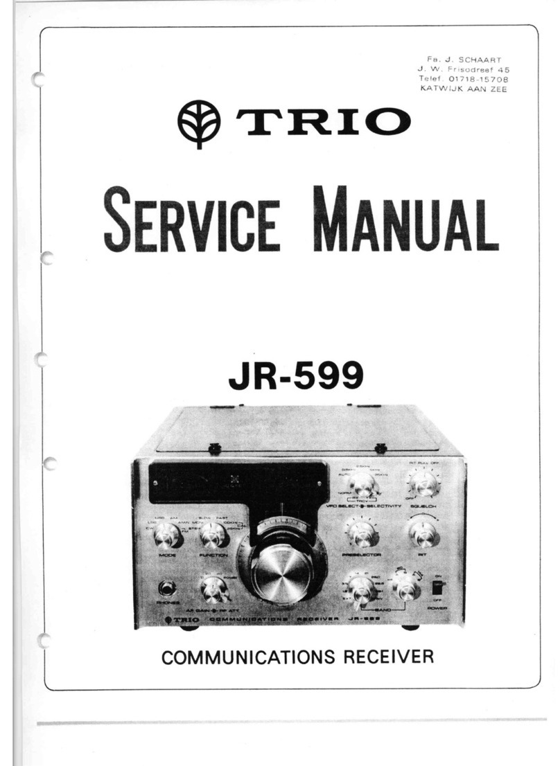
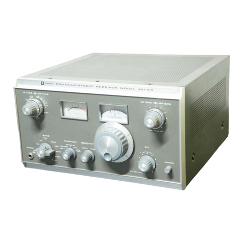
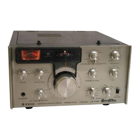
Trio JR-599 User manual

'",
JR-589

~TR.IO
ALL
BAND
SSB
COMMUNICATIONS
~R-599
(I)
The
model
JR-599
is
classified
into
three
models:
CUSTOM
DELUXE,
CUSTOM
SPECIAL (M)
and
CUSTOM SPECIAL (X).
These models may be identified
by
their
name
plates
attached
on
the
front
panels.
The
major
differences
of
these models are
as
shown
in
the
table
below.
Model
IF
Filter
VHF
Converter
CUSTOM
DELUXE
SSB,
FM
Not
equipped
SSB, FM,
CW,
AM
144 MHz
CUSTOM SPECIAL (M)
converter
CUSTOM SPECIAL
(X)
SSB, FM, CW,
AM
50
&144 MHz
converter
RECEIVER
(2)
Optional
filters
and
crystal
converters
are
made
available
at
dealers
of
our
products
for users
to
modify'
sub-models CUSTOM
DELUXE
and
CUSTOM
SPECIAL
(M)
into
models
CUSTOM
SPECIAL
(X) by
their
own
hands.
We
are sure
that
users
can
entertain
themselves
with a
smart
and
pleasantQSO
after
reading
this
manual.
CONTENTS
11111
Iltl
1111:1
'Ill Ilflll"
1111111I11111I1'·1111
II
'Ir!UIIIIIIW"III(JHlI III
tI
1Illftfl
1111I11
ltllll
l/IllllIlllllllIlllll/lIIl1l1llllllU
Iltlllli:lllllllll!llllllllllllllllllllJllllllllllllrtlllllllllllHtllltlUlIIllItIIlI
tllllllllllllll!lIIll11IIl11JllttlllTllllln
Htlll
..
ltlIIIIIIIJUtItIIllIIlI
Special
Features....................................................
2
Circuit Description :........
..
3
Controls and their Functions : . . . .
..
10
Operating Instructions . . . . . . . . . . . . . . . . . . . . . . . . . . . . . . . . . . . . . . . . . . . . .
..
15
Accessory Circuitry 22
Alignment :
..
25
Maintenance 27
Schematic Diagram 29
Specifications ....................................................
..
30
1

SPECIAL
FEATURES
Qllmllllllllllllllllllllllllllllllllllllllllllllllllllllllllllllllllllllllllllllllllllllllllllllllllllllllllllllllll1I11111l11111111l11l111111111111111111111111111111111111111111111111l1111111111111111111111111111111111111111111111111111lI111111111l1111111111111l11111111111111l11111111111111111111111111111111111111111111111l11111111l1111
1.
All solid
state
circuits insure high
quality
reception
of
the
amateur
bands
allocated over a
freq
uency
range from 1.8
to
29.7
MHz,
the
50
and
144 MHz
bands
and
WWV's 10 MHz
standard
signal.
2.
Field
Effect
Transistor
(FET)
used as
RF
amplifier
and
mixer - a SIN, cross
modulation
and
image characteristics
better
than
vacuum
tu
be receivers characteristics.
3. IC
employed
as
IF
amplifier provides lligh
stability
and
gain.
....
4.
VFO
employing
FET
provides ahighly-stable,
low noise-factor
output.
5. Precision
type
double
gear mechanism
and
variable
capacitor
with
linear characteristic
provided for main
tuning
dial covering a25
kHz
band
with
its
one
complete
turn
- a
receiving frequency readable
to
the
nearest
500
Hz.
6.
Fixed
channel oscillators self-contained for 5
channels-spot
reception
available for 5specific
frequencies.
7. Amplifier
type
AGC circuit
with
time-constant
selector
switch -distortionless
reception
of
a
high
input
signal, which
is
specifically useful
for SSB signal.
8.
100
and
25
kHz
crystal
controlled
calibrator
circuits
incorporated
-precise frequency
calibration available for every
one
complete
turn
of
main
tuning
.dial as well as for use
of
this
set
as afrequency measuring set during
~SO.
9. Receiver incremental
tuning
(RIT)
circuit in-
corporated
provides
means
for fme
adjustment
of
receiving frequency
or
correction
of
a
tuned
frequency
without
manipulation
of
main tun-
ing dial during a
combined
transmitter-receiver
operation,
as practised using a
mated
trans-
mitter.
10. Ring, linear
and
ratio
detectors
equipped
for
SSB,
AM
and
FM signal
receptions
respectively.
11. Crystal
and
LC filters serving as
IF
filters for
SSB
and
FM
receptions
respectively, are easily
selected as desired by means
of
aMODE switch
depending
on
the
condition
of
radio inter-
ference with aSELECTIVITY
switch
placed in
AUTO
position
to
interlock
its
electron
switch
with
the
MODE switch.
"An
additional crystal
filter
incorporated
in model CUSTOM SPE-
CIAL
-for
AM
reception."
12. Beat frequency oscillator (BFO)
operated
under
control
of
crystals for
both
SSB
and
CW
receptions with an electronic switch provided
for selection
of
an
appropriate
crystal.
13.
RF
attenuator
inserted
in
antenna
input
circuit
to
provide
means
for
adjustment
of
RF
gain
by
0, 20,
40
and
60
dB
steps, as selected using a
selector
switch -
enables·
model
JR-599
to
serve as afield
strength
measuring set.
14.
Output
transformerless (OTL)
type
audio
frequency
circuit
adopted
-high
power
output
with low
distortion
factor
available.
15.
Operable
from an AC 100, 117,
220
or
240
V
source as well as aDC 12 Vsource, as selected
by means
of
avoltage
selector
switch.
16. Provision
is
made for
mounting
a
50
and 144
MHz crystal converters. [Model
CUST9M
SPE-
CIAL (M) self-contains a144 MHz
converter
and Model CUSTOM SPECIAL (X)
both
50
and 144 MHz converter.]
17. A
combined
transmitter-receiver
operation
available when
operated
in
conjunction
with
model
TX-599
Transmitter,
a
combination
transmitter
for
model
JR-599
Receiver.
18.
An
extremely high-degree transmiHer-receiver
operation,
or
the
so-called cross-operated
VFO,
is practicable when a
combination
of
model
JR-599
Receiver
and
Model
TX-599
Trans-
mitter
are
operated
with their VFOs placed
under
control
of
the
mated
sets.
19.
Communication
speaker
"SP-55"
made
avail-
able
to
insure higher-quality reception.
2

The block diagram
of
model JR-599 Receiver
is
as
shown
in
Fig. 1. This receiver generally operates
on
the
double
superheterodyne
system, in which
the
receiving signals ranging from 1.8
to
29.7
MHz
including the WWV's 10
MHz
standard signal are
converted by the 1st mixer
into
the 1st
IF
signals
ranging from 8.295
to
8.895 MHz, which are
further converted by the 2nd mixer
into
the 2nd
IF
signal
of
3.395 MHz.
For
the
receiving signals
of
50 and 144
MHz
the receiver operates
on
the
triple superheterodyne
system, in which the receiving signals are converted
initially
by
acrystal converter
into
the 28 MHz
band signals before they are applied
to
the
RF
unit.
1.
RF Unit (UC1120J)
The
signal entered from the
antenna
passes
through the protective diodes to the ANT coil
of
this
RF
unit selected
in
accordance with the
frequency band
to
which the signal belongs.
The
ANT coils are provided independently for
all
receiving bands to insure the supreme performance
of
the receiver set.
The
signal passing through the ANT coil
is
applied to
RF
amplifier Q1 comprising field effect
transistor
(FET)
3SK22, where
it
is
amplified
enough.
An FET, featuring a
better
cross modulation
characteristic and ahigh
output
impedance com-
pared with ordinary transistors, enables the
RF
coil
inserted succeeding to
the
RF
amplifier to provide
ahigher
Q.
The
RF
coils, similady to
the
ANT coils, are
provided independently for all receiving bands and
mounted
as acoil pack
on
aprinted circuit board.
The
amplified
RF
signal
output
ranging frbm
1.8
to
29.7 MHz
is
applied via
the
RF
coil selected
corresponding
to
the receiving band
to
gate 1
of
1st
mixer Q2,
to
which the 1st local oscillator voltage
111111111111111111111111111111111111111111111111111111111111111111111111l1l11l11l11111111111111111111111111ll111111111111111111l111111111l11l1Illllllllll1111111111111'1l11111111111111l1111111111IlJllllllJll11111l1J1111l111111l1111l11111111111111111l111l1111l1111111l111lIllllllllllllllll1JllllllllllllllllllllllllllllllllllJllllllll1flllll
VR
POWER
AMP
RING
DET
Xn3393.5kHz
X,,3396.5 "
X,,3395.0 "
AM
1----l<:l-f-+-_-jD)l-E_T~
~
l.-...,....--J
L{>I-J
FM
ANL
Block
Diagram
Fig.
1
t--
__
~BUFFER
r:::::::::::L
.1.
.L
~
=r----T
OSC
4.9-55MHz
5.5-4.9MHz
TO
TX
VFO
X,
29.
895MHz
X,36.895 "
X.37.395 "
X,37.995 "
X,,18.895 "
OSC
OUTI
~I
~BUF~ER
I
OSC
...I. .J.
=
-----
=
T T
HETERODYNE XTAL
(X,-X,,)
Xl
-------
X,l
O.695MHz
S'r
X,12.395 "
X,15.859 "
X,22.895 "
r-----~
I
2M
I
XTAL I
:CONVERTOR
I
L
...1
r
C>-r
__
6M
__
~-'J
r
WXTAL U
ICONVERTORI
L
...J
IlllllllllI11111111l11111111111lllll1rllllllllllllllllllllll1111111111111111111111111111111111111111111111111111111111111111111111111:11111111111111111111111111111111111111111111111111111111111111111111111111111111111111111111111111111111111111111111111111111111111111111111111111111111111111111IIIIIIIII1IlllllltlNIlIIIIIIIIIIIII1ll111
3

is
injected
through
ga
te
2.
Thus, 1st
mixer
Q2
comprising
FET
3SK22
heterodynes
its
input
signal with Ist local oscillator
outpu
t
to
deliver
the
1st IF signal ranging from
8.295
to
8.895
MHz.
Ist local oscillator Q3
is
an
overtone
oscillator
employing
type
2SKl9
FET,
to
which avoltage
of
9V
is
supplied as
the
Bvoltage from
the
regulat-
ed
power
supply.
The
oscillation coils and crystals provided for
1
st
local oscillator Q3 are
incorporated
in acoil
pack.
The
output
signal
of
1st local oscillator Q3
is
taken
out
from
the
collector
of
oscillator transistor
and applied
to
1st
mixer
Q2. Part
of
the
output
is
fed
through
buffer
Q4 comprising
type
2SC460
transistor
to
the
remote
terminal.
Buffer
Q4
lowers the
impedance
of
its
input
signal in
order
to
have
the
output
signal sent from
the
remote
terminal
to
the
transmitter
operating
under
a
combined
transmitter-receiver basis serve as the
2nd
mixer
signal.
The
RF
unit
also
incorporates
part
of
the
AGC
circuit
extending
from AGC
control
transistor
Q5
to
the
input
side
of
RF
amplifier Q2,
the
gain
of
which being
automatically
controlled
as follows:
Gates
1
and
2to
RF
amplifier
Ql
are
kept
closed when
no
signal presents with avoltage
of
4V
developing across Zener diode D3, normally based
from the source voltage, and
opened
with the
output
of
AGC
control
transistor Q5 when asignal
presents
to
control
the
gain
of
RF
amplifier Q
1.
In
this case,
FET
used as
RF
amplifier Q1 provides a
better
AGC characteristic
compared
with ordinary
transistors.
2.
IF Unit (UC1212J)
The
1st
IF
signal delivered from 1st
mixer
Q2
in
the
RF
unit
is
fed
to
band pass filter B.P.F. in
this
IF
unit, where
the
unwanted
frequency com-
ponent
of
the
input
signal
is
rejected.
The
B.P.F.
has apass
band
of
600
kHz from
8.295
to
8.895
MHz. .
The
1
st
IF
signal
is
then
applied
to
2nd
mixer
Ql
consisting
of
an
FET
3SK22, where
it
is
heterodyned
with
the
output
signal
of
variable
frequency oscillator (VFO)
to
turn
into
the
2nd
IF
signal. This signal
is
fed once
to
the
filter
unit
and
then
conducted
back
to
the
IF
unit, where
it
is
applied to 1
st
IF
amplifier ICQ2 (TA7045M).
The
2nd
IF
signal ou
tpu
t
of
1
st
IF amplifier ICQ2
is
applied
to
2nd
IF
amplifier Q3 (2SC460), where
it
is
further
amplified.
The
output
signal
of
2nd
IF
amplifier Q3 is fed
to
three
types
of
detector
circuit: aring
detector
comprising diodes D4
~
D7, an
AM
detector
consisting
of
capacitor
C14 (33 PF) and diode D3
(IN60) and a
ratio
detector
comprising adiscrimi-
nator
transformer
connected
succeeding
to
limiter
Q8 (2SC460). Thus,
the
ring
detector
detects
the
SSB and
CW
signals applied as its inputsignals
into
an
AF
signal.
The
AM
detector
detects
the
AM
signal applied as its
input
signal
into
another
AF
signal. While,
the
ratio
detector
ratio
detects
the
FM
signal delivered from limiter Q8 (2SC460)
into
the
third
AF
signal.
Part
of
2nd
IF
amplifier Q3
is
also applied via
capacitor
Cl3
to
an AGC
detector
circuit consist-
ing
of
diodes D1
and
D2 (IN60).
The
detected
output
from
diode
D1
is
fed
to
an AGC amplifier
Q4, where
it
is
amplified
and
applied
to
transistor
Q5
(2SA495)
serving as
both
an
emitter
follower
and a
current
amplifier. Thus, transistor Q5
delivers two
outputs:
One
output,
which is taken
out
from
the
emitter
side for
the
AGC,
is
fed
to
1st
amplifier ICQ2
and
2nd
amplifier Q3
and,
via
resistor
R22
(l0
K.Q),
to
RF
amplifier Q1 in
the
RF
unit. Part
of
the
above
output
is
also fed via
resistor R23
(220
K.Q)
to
squelch amplifier Q6.
While,
the
other
output,
taken
out
from
the
collector
side,
is
directly supplied
to
the Smeter,
thereby
deflecting the
meter
depending
on
the
AGC voltage
detected.
The
time
constant
of
the above
mentioned
AGC circuit is
determined
by time
constant
capaci-
tor
C3
inserted succeeding
to
AGC amplifier Q4
but
outside
the
IF
unit.
The
rise-up
of
the
AGC circuit depends
on
the
collector-emitter resistance
of
AGC amplifier Q4
when amplifier transistor
Q4
conducts
and
the
operation
of
the
above-mentioned time
constant
capacitor
Q3.
When the AGC circuit
is
started
by
the
output
of
2nd
IF
amplifier Q3, AGC amplifier
Q4
offers a
low impedance against time
constant
capacitor
C3
because
of
its
current
amplification characteristic
and, therefore,
conducts
at
once
owing
to
the time
constant
capacitor
C3
discharged momentarily.

When
the
output
of
2nd
IF amplifier
is
cut
off, on
the
contrary, AGC amplifier Q4 increases its
impedance against time
constant
capacitor C3,
thereby bringing itself
to
the
cut-off
condition
slowly because
of
capacitor
C3
charged gradually.
Thus,
it
follows
that
AGC amplifier
Q4
provides an
ideal quick-start slow-release characteristic for its
operation.
(Note
that
the
above-mentioned AGC
operation
applies to acase where the FUNCTION
switch
is
placed in
the
(AGC)
FAST
position for
the
quick AGC operation.
For
the
(AGC) SLOW
position
of
FUNCTION switch AGC amplifier
Q4
provides an AGC characteristic
just
opposite
to
the
above characteristic because
of
the
discharge and
charge
of
time
constant
capacitor C3
conducted
reversely.)
By
the
way,
the
output
of
AGC transistor Q5
applied via resistor R23 to squelch amplifier Q6
(2SC733)
is
amplified there and
then
applied
to
the
base
of
buffer transistor Q7 (2SC733),
thereby
controlling
the
base voltage with
the
input
signal.
As aresult, buffer transistor Q7 controls
AF
amplifier
Ql
in the
AF
unit with its
output
to
perform asquelch
operation
under
control
of
the
inputsignal.
Buffer transistor Q7,
mentioned
above, also
acts as
an
emitter
follower providing ahigher
impedance
to
conduct
the
detected
SSB,
CW,
AM
or
FM signal with alower impedance
to
the
AF
volume control outside the
IF
unit,
as
selected by
the
MODE switch from
the
2nd
IF
amplifier Q3
output.
3.
Filter Unit (UC1213J)
The
filter
unit
is inserted outside
the
IF
unit
between
the
output
of
2nd
mixer
Q2 and
the
input
of
1st
IF
amplifier Q2 in
the
latter
unit.
This
unit
incorporates four fllters with diode
switches provided for
the
SSB,
CW,
AM
and FM
signals respectively. These filters are so designed
that
an
appropriate
filter
is
selected by means
of
a
diode switch when the MODE switch
is
placed in
the position for adesired receiving signal.
Now, suppose
that
the
MODE switch
is
placed
in
the
SSB position for reception
of
the SSB
signal. This applies avoltage
of
13.8 V
to
the SSB
terminal for
the
diode switch
of
filter
XF-l.
This
causes a
current
to
flow from the terminal through
resistor RI
(220
D)
in
the
two directions to
resistors R2 (4.7
kD)
and R3
(220
D).
Thus, the
5
current passing resistor R2 flows
as
the
forward
current
through
diode D1
(l
N60) and resistor R21
(1
kD)
to
the
earth. While, the
current
passing
resistor R3 flows as
the
forward
current
through
resistor
R4
(4.7
kD),
diode D2
(lN60)
and resistor
R22
(1
kD)
to
the
earth.
Under
the
above condi-
tion apositive voltage
of
approx. 2.3 V
is
built
up across resistors R21 and R22 to the earth. This
applies abackward voltage
to
diodes D3 through
D8
(l
N60). As aresult, diodes D1 and D2 turns
ON and diodes D3
through
D8 turns
OFF,
thereby
allowing only
the
SSB signal
to
pass
through
fllter
XF-l
from 2nd
mixer
Q1
to
1st
IF
amplifier Q2.
The ratio
of
the
signals
under
the above ON and
OFF
conditions
of
the
diodes
is
approx.
70
dB.
The
XF-l
filter requires
an
external resistance
of
4.7
kD
and an external capacitance
of
33 pF.
Hence,
the
filter is so designed
that
it
employs the
DC
resistors for diode switch as
the
external
resistance
of
4.7
kD
and
the
internal capacitances
of
the
printed
circuit board and coils
L1
and L2
(l
mH),
the
capacitance
of
lead wires and
other
stray
capacitance as
the
external capacitance
of
33 pF.
Other
filters for
the
CW,
AM
and FM signals
XF-2, XF-3 and aLC circuit are selected by their
diode switches
just
in
the
same
manner
as describ-
ed above when
the
MODE switch is placed in
the
CW,
AM
and FM positions, respectively.
4.
VFO
Unit (UC0116J)
The
VFO
Unit
incorporates avariable frequen-
cy oscillator circuit, which delivers
the
output
frequencies varied over afrequency range
of
600
kHz from 5.5 to 4.9 MHz
to
the
2nd
mixer in
order
to convert
the
l.st
IF
signals ranging from
8.895 to 8.295 MHz
into
the
2nd
IF
signal
of
3.395 MHz.
Asub-dial scale is calibrated for
the
above
frequency range from graduation 0
to
gradation
600
at
intervals
of
1kHz.
The
variable frequency osicllator consists
of
oscillator transistor Q1 (3SK22) arranged
as
a
modified Clapp socillator circuit and
operate
quite
stably with
buffer
transistor Q2
(2SKI9).
The
output
of
variable frequency oscillator
is
deliversed through buffer transistor Q2 and one
stage
of
harmomic filter to
the
output
circuit, a
Darlington circuit comprising amplifier transistors
Q3 and Q4, Hence, the
output
circuit operate
stably against
the
variation
of
its load.

The
YFO
unit
also
incorporates
areceive
incremen
tal
tuning
(RIT)
circuit.
The
RIT
circuit
is
operated
from
the
RIT
voltage
generated
in its
generator
circuit, which
is
incorporated
in
the
UC I0 I
OJ
Unit
and
actuated
by
areceiver relay during
the
reception
under
the
combined
transmitter-receiver
operation,
and
varies
the
YFO
frequency
regardless
of
the
setting
of
YFO
SELECT
dial.
The
RIT
control
on
the
front
panel provides
means
for
controlling
the
above-
mentioned
RIT
voltage.
Note
that
the
YFO
Unit
should
never be
removed
from
its case
or
modified
internally
since
its
adjustment
needs ahigh degree
of
adjustment
technique.
5.
Carrier (BFO)
Unit
(UC1214J)
The
carrier
unit
incorporates
abeat
frequency
oscillator
(BFO)
circuit.
The
BFO
circuit, consisting mainly
of
oscillator
transistor
Q2
(2SC460),
buffer
transistor Q2
(2SC460)
and crystals
X-I,
X-2
and
X-3
with
a
diode switch consisting
of
diodes DI
through
D4
(I
SI555),
inserts a
beat
or
carrier
frequency
in
the
ring
detector
for
reception
of
the
SSB
or
CW
signal.
Oscillator
transistor
Q2
is
the
Pierce B-E circuit
and its
output
frequencies are
adjusted
by
means
of
trimmer
capaci
tors
TC
I
through
TC3 inserted in
parallel with crystal X I
through
X3 respectively.
Selection
of
acrystal for
the
BFO in
reception
of
the
CW,
LSB
or
USB signal
is
performed
by the
above-mentioned
diode
switch as follows:
Suppose,
for
example,
that
the
MODE
switch
is
placed
in
the
LSB
position
for
reception
of
aLSB
signal. This applies a
power
supply
voltage
of
13.8
Y
to
the
LSB
terminal
of
the
Carrier (BFO) Unit.
As aresult, aforward voltage
is
applied from
the
LSB
terminal
through
resistor
R4
(22
kS1)
and
choke
coil
L4
(I
mH)
to
diode
D4
(I
S1555), there-
by
conducting
the
diode
since
the
diode
offers
alow
internal
resistance
because
of
the
voltage applied.
This in
turn
inserts crystal
X3
connected
in series
with
the
diode
via
capacitor
C6
(22
pF)
across
the
base
and
emitter
of
oscillator
transistor
Q
I.
Hence, oscillator
transistor
Q I
starts
in oscillation
at
the
X3 crystal
frequency,
or
3393.5
kHz.
The
beat
frequency
oscillator
operates
just
in
the
same
manner
as
mentioned
above
for
reception
of
the
USB
or
CW
signal. But, its
center
frequency
3.395
MHz
is
shifted
by
700
to
800
Hz
for
reception
of
the
CW
signal because the
center
frequency
zero beats
with
the
ou
tput
signal
of
2nd
IF
amplifier Q3 in this case owing
to
the fact
that
the
output
signal'
is
continuous
wave,
and
this
makes
it
difficult
to
receive
the
incoming
frequen-
cy.
The
above-mentioned
shift
of
the
YFO
frequen-
cy
is
accomplished
by
the
diode
switch
as follows:
When
the
MODE
switch
is
placed
in
the
CW
position,
aDC voltage
is
applied
from
the
CWR
terminal
of
this carrier
unit
via resistor
RI
(2.2
kS1)
and
choke
coil
Ll
(I
mH)
to
diode
DI,
turning
the
diode
ON. This
grounds
crystal X2
through
the
diode
without
any
capacitor
and,
therefore,
insert
the
crystal directly across the base
and emi
tter
of
oscilla
tor
transistor
QI. As aresult, .
oscillator
transistor
Q2
starts
in oscillation at a
frequency
alittle
lower
than
the crystal frequen-
cy.
The
beat
tone
for
the
CW
reception
may
be
adjusted
through
the
use
of
trimmer
capacitor
TC
I, which provides
means
for
varying the BFO
frequency
by
±200
Hz.
The
output
of
BFO
oscillator
transistor
Q I
is
applied via avoltage divider circuit comprising
capacitor
CII
(10
pF)
and
CI3
(22
pF)
to
buffer
transistor Q2.
Buffer
transistor
Q2,
acting
as an
emitter
follower, offers an
output
impedance
as
low as a
bout
100
S1,
thereby
minimizing variation
of
the
output
voltage
and
frequency.
6.
25 kHz /100
kHz
Marker
Unit
(UC1505J)
The
25
kHz
/
100
kHz
marker
unit
incorpo-
rates a
marker
signal
generator
circuit which
generates a
marker
signal over a
frequency
range
from
3.5
to
28
MHz
at
intervals
of
25
or
100
kHz
for
calibration
of
the
main
tuning
dial. Selection
of
a
25
or
100
kHz
marker
signal
may
be
accomplished
by
means
of
the
FUNCTION
switch.
The
marker
signal
generator
circuit
consists
mainly
of
four
transistors Q I
through
Q4
(2SC373)
and
one
100
kHz
crystal
(HC/!3U).
Transistor
Q
1,
acting
as
an
oscillator, oscillates
,«ith
the
1
00
kHz
crystal
at
a
frequency
of
100
kHz.
Trimmer
capacitor
TC
I
inserted
in ,the
collector
circuit
of
oscilla
tor
transistor
Q I provides
means for fine
adjustment
of
the
oscillator fre-
quency.
The
output
of
oscillator
transistor
Q I
is
fed via
capacitor
C4
(33
pF)
to
diode
DI,
through
which
6

it
is
shaped
into
apulsed wavefonn occuring
at
a
period
of
one
fourth
the
100 kHz and drives a
free-running multivibrator consisti.ng
of
transistors
Q2 and Q3 at aperiod
of
just
25
kHz since the
multivibrator has afree-running period
of
about
25
kHz.
The
output
of
the
multivibrator
is
applied to
amplifier transistor Q4,
through
which
it
is
shaped
in the rectangular wavefonn and delivered to
RF
amplifier Q1 in the
RF
Unit.
When
the
FUNCTION switch
is
placed in the
100 kHz CAL position
the
emitter
of
transistor Q2
is
grounded via
the
MS
terminal
of
this unit,
turning transistor Q2 off. This disables the multi-
vibrator
and
allows transistor Q3
to
operate as a
mere amplifier. As aresult,
the
100 kHz pulsed
signal from
the
oscillator transistor are
conducted
as
they
are to amplifier transistor Q4 and, there-
fore,
to
RF
amplifier Q
1.
7.
Regulated
Power
Supply Unit (UC1010J)
The
regulated
power
supply
unit
provides
necessary operating voltages for the VFO, BFO and
1st local oscillator. Especially,
it
supplies avoltage
with least variation to
the
VFO (including the
RIT
circuit)
to
prevent
the
VFO from changing its
oscillator frequency with variation
of
the supply
voltage.
The
unit
consists mainly
of
four transistors Q1
(2SA497),
Q2
(2SC373), Q3 (2SC372) and Q4
(2SC372) and reference diode D1 (RD6A).
Transis
tor
Q1
is
the current
con
trol transistor,
which controls the
input
current
in accordance
with
an
error
voltage. Transistors Q2 and Q3 are
the
error
voltage amplifier transistors. Transistor
Q4
is the
error
voltage
detector
transistor and also
serves as
the
temperature-characteristic cancelling
transistor for transistor Q3. Diode D1 (RD6A) is
the
zener diode for producing areference voltage.
The
error
voltage
detected
by
error
voltage
detector
Q4
is
amplified
through
two amplifier
stages
of
transistors
Q2
and Q3. This allows
the
regulated
power
supply
unit
to
provide
an
ex-
tremely excellent voltage stability.
The
voltage stability due
to
a
temperature
change depends
on
the
temperature
characteristics
of
the reference voltage diode and the error voltage
amplifIer circuit.
The
reference voltage diode used is zener diode
RD6A, which has a
temperature
coefficient
of
O.
7
While,
the
error
voltage amplifier circuit consists ot
amplifier transistors Q2 and Q3 with transistor Q3
coupled
through
differential
connection
to
error
voltage
detector
diode Q4, and offers least varia-
tion
of
its characteristic due
to
temperature
change
because transistors Q3 and
Q4
cancel their tem-
perature characteristics.
Further,
current
control
t,dnsistor Q1 suffers from
almost
no
change
of
its
characteristic due
to
temperature change because it
is
asilicon PNP transistor.
In
addition,
this regulated power supply
unit
is
so arranged
that
it
protects
current
control
transis-
tor
Q1 against
an
excessive currentwhich might be
flowed through
the
transistor when the
output
terminal
is
shorted
to earth, as
encountered
in
ordinary regulated
power
supply circuits.
Resistors RIO
and
R
11
and variable resistor
VR2 are provided to
produce
necessary
RIT
voltages
to
be fed
to
the
RIT
circuit in
the
VFO
unit.
8. AF Unit (UC1307J)
The
AF
unit
incorporates
an
AF
amplifier
circuit to
operate
the
speaker. This amplifier
circuit amplifies
the
AF
output
delivered via
variable resistor
VR4
(l0
kn),
or
the
AF
volume
control, from squelch
buffer
transistor Q7, which
is
connected
through the MODE switch and detec-
tor
circuits to 2nd
IF
amplifier transistor Q3.
The
AF
amplifier circuit, consisting mainly
of
four amplifier transistor Q1 (2SC733), Q2
(2SC734), Q3 (2SD90) and
Q4
(2SB473), operates
as follows:
The
AF
signal from squelch
buffer
transistor
Q7
is
conducted
from
the
IN terminal
of
the unit
via capacitor
Cl
to
amplifier transistor Q
1,
where
the
signal
is
amplified on
the
voltage amplification
basis.
The
output
of
amplifier transistor
Ql
is
amplified by amplifier transistor Q2 on
both
the
voltage and
power
amplification bases.
The
output
signal from amplifier transistor Q2
is
applied to a
power
amplifier consisting
of
transistors Q3 and
Q4, where it
is
amplified
on
the
power
amplifica-
tion basis. Since transistors Q3 and
Q4
are coupled
through a
comprementary
connection
circuit to
the
preceding circuit,
they
form an
output
trans-
formerless (OTL) circuit and, therefore, deliver
the
output
signal with extremely small
distortion
compared with
that
of
the
conventional
power

transformer
transformer
coupled
to
the
preceding
stage. Anegative voltage is fed
back
from
the
joint
of
transistors
Q3 and
Q4
via resistor
RIO
(I
Ok.Q)
to
the
input
side
of
transistor
Q2,
thereby
not
only
reducing
the
disortion
of
output
signal
further
but
lowering
the
output
impedance
with
the
resultant
improvement
of
damping
factor. In
addition,
a
negative DC
current
is
fed back
from
the
collector
of
transistor
Q4
to
the
emitter
of
transistor
Q2
because
of
transistors
Q2,
Q3
and
Q4
connected
in
series
and
this reduces
the
variation
of
the voltage
at
the
joint
of
transistors Q3
and
Q4.
Variable resistor
VR
I
inserted
in
the
collector
circuit
of
transistor
Q2
is
the
semi-fixed
control
VR
Ifor
adjustment
of
the
supply
current
to
transistors Q3 and
Q4
wr.en
no
signal presents.
The
variation
of
the
above
supply
current
is
compensated
by
thermister
TH
1
(5T32)
inserted in
parallel
with
the
semi-fixed
control.
Capacitor
C7
(33
pF)
is avoltage cancelling
capacitor
for
the
negative
feedback
voltage
to
the
collector
side
of
transistor Q2.
9. Fixed Channel
Unit
(UC0113J)
The
fixed
channel
unit
incorporates
oscillator
transistor
Q I
arranged
so as
to
form
aPierce C-G
oscillator
circuit
and
emitter
follower
transistor
Q2
acting
as abuffer.
Oscillator
transistor
Q I
operates
in
conjunction
with
afixed channel crystal selected by the CH
SELECT
switch
among
those which are
mounted
on
a
separate
printed
circuit
board
for
reception
of
the fixed
channel
signals.
The
output
of
oscillator transistor Q2
is
fed
through
emitter
follower
Q2
to
2nd
mixer
Q2,
where
it
is
heterodyned
with
the
fixed channel
.signal
under
reception.
10. Crystal Converter
The
TRIO
model
JR-599
SPECIAL (X) are sup-
plied with
the
50 MHz Crystal
Converter
(CC-69)
and
the
144
MHz Crystal
Converter
(CC-29)
to
provide
means
for
reception
of
the
50
and
144
MHz
VHF
bands.
(A)
50
MHz
Crystal Converter CC-69 (UC-2302J)
The
50 MHz crystal
converter
consists
mainly
of
RF
amplifier QI,
mixer
Q2
and
two
local oscillators Q3 and
Q4,
as
shown
in the
circuit
and
block diagrams given in Fig.
2.
RF
amplifier Q I
and
mixer
Q2
employ
an
FET
2SKI9
and
FET
3SK22
respectively.
Local oscillators Q3
and
Q4,
each comprising
transistor
2SC785, provide local oscillator fre-
quencies
of
22
and
23.7
MHz
for
the
mixer
operating
with
the
Aand B
channel
signals,
respectively.
The
input
signal, i.e.
the
signal
in
areceiv-
ing
frequency
range
from
50 to
51.7
MHz for
channel
A
or
from
51.7
to
53.4
MHz for
channel
B,
is
applied from
the
antenna
to
the
ANT
input
circuit
of
the
converter, from which
it
is
fed
through
RF
amplifier
Q2
to
mixer
Q2.
Thus,
mixer
Q2
heterodynes
the
A
channel
signal
of
50
to
51.7
MHz
with
the
22 MHz
output
of
local oscillator Q3
into
an
HF
signal
of
28 to
29.7
MHz.
For
the
B
channel
signal
of
51.7
to
53.4
MHz,
the
mixer
heterodynes
the
signal
with
the
23.7
MHz
output
of
local
oscillator Q3
into
an
HF
signal
of
28
to
29.7
MHz. These
HF
signals are
then
fed
to
the
input
circuit
of
the
RF
amplifier unit.
A
protective
circuit comprising diodes D I
and D2 is
inserted
in
the
ANT
input
circuit
of
this
converter
for
protection
of
RF
amplifier
and
mixer
comprising
an
FET.
The
RF
amplifier stage
is
operated
under
an
AGC
to
improve the selectivity.
In
addition,
avariable
capacity
capacitor
is
inserted
in
each
tuning
circuit for the
RF
amplifier
and
the
mixer
stages
to
vary the
resonance
frequency
of
tuning
circuit
and
widen its
substantial
pass band
simultaneously
with
selection
of
the
A
or
Bchannel for
improvement
of
the sensitivity
and
selectivity
of
the
converter
(Utility model applied for).
(S)
144
MHz
Crystal Converter CC-29 (UC2301J)
The
144
MHz crystal
converter
consisJs
mainly
of
RF
amplifier QI,
mixer
Q2,
2local
oscillators Q3
and
Q4,
and
tripler
Q5,
as
shown
ll1
the
circuit
and
block
diagrams given in Fig.
3.
RF
amplifier
Q I
and
mixer
Q2
employ
an
FET
2SK19
and
FET
3SK22
respectively.
Local oscillators Q3
and
Q4,
each
comprising
transistor
2SC535, provide local oscillator fre-
quencies
of
I16
and
I17.7 MHz for the
mixer
operating
with
the Aand B
channel
signals,
respectively.
Tripler
Q5,
consisting
of
transis-
8

tor
2SC384, triples the frequency
of
each local
oscillator
output
to
obtain the above-
mentioned local oscillator frequencies.
The
input
signal, i.e. the signal in areceiv-
ing frequency range from 144
to
145.7
MHz
for channel A
or
from 145.7
to
147.4 MHz for
channel
B,
is
applied from the antenna
to
the
ANT
input
circuit
of
the
converter, from which
it
is fed through
RF
amplifier Q1 to mixer Q2.
Thus, mixer Q2 heterodynes the Achannel
signal
of
144
to
145.7
MHz
with the 116
MHz
output
of
tripler Q3,
or
the Achannel local
oscillator frequency,
into
an
HF signal
of
28 to
29.7 MHz.
For
the Bchannel signal
of
145.7
to
147.4 MHz,
the
mixer heterodynes the
signal with
the
117.7
MHz
output
oftripler
Q3, or
the
Bchannel local oscillator frequency,
into
an HF signal
of
28
to
29.7
MHz.
These
HF signals are then fed to the
input
circuit
of
the
RF
amplifier unit.
Aprotective circuit compnsmg diodes D1
and D2
is
inserted in the ANT
input
circuit
of
this converter for protection
of
RF
amplifier
and
mixer, comprising
an
FET
respectively.
The RF amplifier stage
is
operated under
an AGC to improve the selectivity.
In addition, avariable capacitor diodes
is
inserted in each tuning circuit for the
RF
amplifier
and
the mixer stages
to
vary the
resonance frequency
of
tuning circuit and
widen its substantial pass band simultaneously
with selection
of
the
A
or
Bchannel for
improvement
of
the sensitivity and selectivity
of
the converter (Utility model applied for).
1l1111111111111ll11l111ll11ll1ll1ll111ll11ll111ll11111tllllllllllllllIIlIllIIIll1ll1llllllllllllllllllllllll1I111111111ll1l111111111ll111l1111ll1ll1ll1l1ll1ll1ll1l1ll1ll1ll111l1111ll111l1l1l11111111111l1ll1ll1l11111111l11l1ll1l1l11l1111111ll11l1111111111111111111111l111ll11ll11l1111111111111111111111111111111111Il1tllltltllllllll111111l
ACHANNEL
BCHANNEL
OUTPUT
FREQUENCY
50MHz
~517MHz
51.7MHz·~
53.4MHz
23.7MHz
(b)
Block
.
ANT
Fig.
2
50
MHz
Crystal
Converter
(CC·69)
ACHANNEL
BCHANNEL
OUTPUT
FREQUENCY
28MHz
-29.
7MHz
144MHz
~
145.7MHz
145.7MHz
~
1474MHz
(bl
Block
/
ANT
Fig.
3
144
MHz
Crystal
Converter
(CC·29)
IlrurnrffllOllllrlllllllllllllllllllllllllllllllllllllllllllllllllllllllll11Illlllllllllllltlllllllllllllllllllllllllllll1l11l11111111111111lUI111111111111111111111111111111111111111111111111111I11111111llllllllllltlllllllllllllllllllllllllllllllllllllllllll111111111I11111111111111111111111111111111111111111111111111111111111111111"
9

CONTROLS
AND
THEIR
FUNCTIONS
Front
Panel
Controls
(Photo 1)
(1)
BAND
(Main Band Selector Switch)
Main band selector switch BAND, a 10-
position
rotary
switch provides means for
selection
of
adesired receiving band among
the
8bands allocated over afrequency range from
1.8
to
29.1 MHz
the
WWV's
10 MHz standard
signal
and
an
external band.
select either HF or VHF band as the operating
band. When this switch
is
placed in the HF
position,
it
makes
the
main band selector
switch effective
to
select any band for recep-
tion as mentioned in item
(1)
above. In
other
positions,
the
switch inserts a50 or 144
MHz
crystal converter in the receiver circuit for
reception
of
the 50 or 144 MHz band respec-
tively. (Note
that
this switch
is
ineffective on
model JR-599 CUSTOM DELUXE provided
that
the
model
is
operated with
no
50 or 144
MHz
crystal converter mounted additionally.
This
is
because said model
is
marketed without
the
converter.)
(3) POWER (Power Switch)
The POWER switch provid power ON-OFF
control
to
the
receiver. In
the
ON position,
it
applies power
to
the
power supply circuit and
places the receiver in the runing condition.
(2)
BAND
(Auxiliary
Band Selector Switch)
Auxiliary band selector switch BAND, a
5-position
rotary
switch, provides means
to
(4)
RIT
(Receiver Incremental
Tuning
Control)
Control RIT provides means for fine adjust-
®
®
BANC
......
(JI
a"",
CD
®
(])
-JA-
•••
;==~;;;;;;;;;r_-;r-~~==-;;;i----
cID
l"r...,-:=~~---
®
@
@
®®
@----
===,.l'1':
@
----~=-====-~d1
Photo
1
Front
Panel
10

ment
of
arecelvmg frequency when this
receiver
is
operated
with model TX-599 Trans-
mitter
as acombined transmitter-receiver.
If
the user wantto operate this receiver
on
the
QSO basis, set up
the
receiver and model
TX-599 for acombined transmitter-receiver
operation.
Then,
set the BAND switches and main
tuning
dial
on
the receiver for the riominal
transmitting frequency
of
adesired
partner
station
with
the
RIT switch placed in position
O.
Tune
the receiver
to
the actual transmitting
frequency
of
the
partner
station and proceed
to
the
QSO operation.
If
the receiving frequency shifts during the
QSO operation, re-tune the receiver to the
current
receiving frequency by turning the
RIT
control
to
and
fro, instead
of
manipulating the
main tuning dial. Otherwise, the transmitting
frequency
of
the local station will be shifted.
(5) PRESELECTOR (RF
Amplifier
Tuning
controll
The PRESELECTOR switch
is
the tuning
control
for
the
RF
amplifier stage
of
this
receiver. This control should be adjusted until
the
receiver provides the maximum sensitivity.
(6) SQUELCH (Squelch Control)
The
SQUELCH control serves as the ON-
OFF
control for
both
the squelch and RIT
operations.
That
is, turning this control clock-
wise from
the
OFF
position intensity
the
squelch control to the
IF
output
until the
audio frequency circuit
is
disabled for regenera-
tion
of
the
incoming signal.
While, pulling the
knob
of
this
control
out
of
its normal position turns the RIT switch off.
(7) (8)
VFO
SELECT -
SELECTIVITY
(Composite
VFO
and Selectivity Selector Switch)
The
VFO SELECT -SELECTIVITY con-
trol
is
acomposite switch consisting
of
aVFO
and selectivity selector switches.
The
VFO SELECT switch, a4-position
rotary
switch forming the
upper
knob
of
the
VFO SELECT-SELECTIVITY switch, provides
means
to
select adesired VFO
under
the
combined transmitter-receiver operation
of
models
JR-599
and TX-599. Normally, this
switch should be
kept
in the NORM position.
11
The
SELECTIVITY switch, a5-position
rotary
switch forming the lower
knob
of
the
VFO SELECT-SENSITIVITY switch, provides
means
to
select an
adequate
IF
band
depending
on
the
type
of
emission for the signal
under
reception
of
the
condition
of
radio inter-
ference. In
other
words, this switch should be
placed
at
aposition for which the speaker
delivers
the
sound
output
which
is
most easy
to
hear.
(9) (10)
AF
GAIN
-RF
ATT
(Composite
AF
Gain-
RF
Attenuator
Selector Switch)
The
AF GAIN -
RF
ATT control
is
a
composite switch consisting
of
an
AF
GAIN
control and an
RF
ATT switch.
The
AF GAIN control, acontrol forming
the
upper
knob
of
the
AF
GAIN -
RF
ATT
switch,
is
the
volume control for the speaker
output.
Turning this control clockwise
in-
creases the volume
of
speaker
output.
The
RF
ATT switch, a4-position
rotary
switch forming
the
lower
knob
of
the AF
GAIN -
RF
ATT
switch, provides means to
insert aresistance
attenuator
of
60
dB
at
20
dB
step in the
input
circuit
of
the
RF
amplifier
stage. Using this switch, therefore, model
JR-599
may be used
to
make measurent
of
a
field intensity.
(11) PHONES (Phone Jack)
The
PHONES
jack
is
provided for connec-
tion
of
ahead
phone
plug.
(12) FUNCTION (Function Selector Switch)
The
FUNCTION switch, a6-position
rotary
switch, provides means
to
place model JR-599
under
adesired functional condition such as a
stand-by operation, monitor, sJow and fast
responses and calibration, as obtained by turn-
ing the switch in the STABY, MONI, SLOW,
FAST, 100 kHz and
25
kHz positions respec-
tively.
(13) MODE (Receiver Mode Selector Switch)
The
MODE switch, a6-position
rotary
switch, provides means to select an adequate
mode
of
the receiver operation depending on
the
type
of
emission
of
the signal
to
be
received.

t
(a)
CW
(Continuous
Wave)
Switch
position
CW
is
provided
to
operate
the
receiver
on
an
incoming
con-
tinuous
wave for
reception
of
the
Morse
telegraph
codes.
(b)
LSB
(Lower
Side
Band)
Switch
position
LSB is
provided
to
opera
te
the
receiver
on
an
incoming
LSB
signal for
reception
of
the
3.5
and
7.5 MHz
bands. This
is
because
it
is
an
international
custom
to
use
the
LSB
of
SSB signal for
transmission
and
reception
of
the
3.5
and
7
MHz bands.
(c) USB
(Upper
Sideband)
Switch
position
USB
is
provided
to
operate
the
receiver
on
an
incoming
USB
signal for
reception
of
the
bands
above
the
14 MHz
band.
This
is
because it is ageneral
rule
to
use
the
USB
of
SSB signal
for
trans-
mission and
reception
of
the
bands
above
the 14 MHz
band.
Users
should
be careful
enough
not
to
select a
wrong
sideband
signal for
reception
of
aSSB
band.
Otherwise,
the
receiver fails
to
damodulate
the
incoming
signal
at
all.
(d)
AM
(Amplitude
Modulation)
Switch
position
AM
is
provided
to
operate
the
receiver
on
an
incoming
ampli-
tude-modulated
signal for
reception
of
the
radiotelephone
speech.
If
the
receiver
is
operated
on
an incom-
ing
SSB signal
with
the
MODE
switch
placed
in
this
AM
position
by
mistake,
the
speaker
mere
numbles
out
its
sound
out-
pu
1.
When
operating
the
receiver
with
the
incoming
signals belonging
to
the
bands
below
7MHz
band,
therefore,
never fail
to
turn
the
MODE
switch
in
the
LSB posi-
tion.
For
the
signals belonging
to
the
14
MHz
band
or
higher,
turn
the
switch
in
the
USB
position.
(e) AM.N
(Automatic
Noise
Suppression)
Switch
position
AM.N is
provided
to
suppress
the
annoying
pulsed
noises
due
to
the
atomospherics,
motor
cars engine
and
so
on
appealing
in
the
sound
output
of
speaker
during
reception
of
an
incoming
signal from
an
AM
station.
(f) FM
(Frequency
Modulation)
This
is
the
switch
position
provided
to
operate
the
receiver
on
an
incoming
FM
signal
with
the
built-in 50
or
144
MHz
crystal
converter
inserted
in
the
receiver
circui
1.
(14) S
METER
The
S
METER
indicates
the
level
of
the
signal
under
reception,
as read
on
its scale
in
dB.
The
scale
is
so
calibrated
that
the
meter
reads
40
dB
when
it
deflects
to
graduation
S-9.
(15) Sub-dial Scale
The
sub-dial scale
is
the
disc scale
mounted
below
a
rectangular
small
window
at
the
upper
center
section
of
front
panel.
The
scale bears
the
blue
and
orange gradua-
tions
which,
starting
with
the
zero
blue gradua-
tion,
are
calibrated
alternately
around
the
circumferenece
of
the
disc
for
a
frequency
range
from
0
to
600
MHz
at
intervals
of
25
kHz.
This scale, being
mounted
on
the
shaft
of
the
main
tuning
dial,
shifts
its
position
by
one
graduation
for
everyone
complete
turn
of
the
tuning
dial,
or
a
frequency
band
covering 25
kHz.
(16) Main Dial Scale
The
main dial scale
is
the
disc scale
tightly
kept
in
position
against
the
bottom
side
of
the
main
tuning
dial
with
spring
pressure.
The
scale bears
the
black
and
red gradua-
tions,
which,
starting
with
the
zero
black
graduations,
are
calibrated
around
the
entire
circumference
of
the
disc for
frequency
ranges
from 0
to
25 kHz
and
25
to
50
kHz,
the
former
being
marked
with
black figures
and
the
latter
red figures. Hence,
it
provides
means
for
indicating
the
receiving
frequency
to
which
the
receiver
tuned
through
the
use
of
the
main
tuning
dial.
Because
of
its
constructional
characteristic,
this
scale
may
be
calibrated
quite
easily by
12

shifting its zero graduation
to
a
point
for which
the
receiver zero beats with the calibration
signal while depressing
and
turning
it
with
the
black
knob
incorporated
to
the main tuning
dial below the dial knob.
(17) Main
Tuning
Dial
The
main tuning dial
is
the
knob
with
the
main-dial
and
su
b-dial scales in terlocked
wi
th
its shaft.
This dial provides means
to
tune
the
receiver circuit with adesired band signal
within a
band
width
of
600
kHz, for which
it
shifts the main-dial
and
sub-dial scale gradua-
tions
by
25 kHz for
everyone
complete
turn
of
its knob.
Note
that
this dial is
stopped
at
a
point
when
rotated
outside the 0
to
600
kHz
range
of
the
su
b-dial scale. Do
not
try
to
rotate
the
dial
beyond
the
above point. Otherwise,
the
double gear mechanism for the dial may be
damaged.
Rear Panel
Controls
and
Terminals
(Photo
2)
(1)
HF
ANT
This
is
the
antenna
terminals provided for
exclusive use
with
HF
antenna
having an
impedance
of
50
to
75n
and
providing a
receiving
band
from 1.8
to
28 MHz.
(2) SPEAKER
This
is
the
AF
output
terminals provided
for
connection
of
an external speaker. This
terminals have an
output
impedance
of
8n,
but
speakers
with
voice coil
of
4 -
16n
are also
available.
(3) REMOTE
The
REMOTE terminals are the connecting
terminals for a
transmitter
to
be
operated
in
combination
with
this receiver.
When this receiver
is
to
be
operated
with
model TX-599
Transmitter,
connect
between
the
REMOTE terminals
of
the
receiver and
IlllllllllllllllllllllltllllllllllllllllllllllllllllllllIlltlllll'III'llll"III"IIII"lllllllllllllll'lllllllIllllllllllllIllllllllllllllll'll,llllllllllllllllllllIltlllllllllllllllllllllllll.,rllllllllll"IIIIIllllll1111111111,"llllllllllll"lll'llllllllllllllltlllllll11111'llllllllllllllllllllllilllllll'lllllllllllllllll11111\111111
®®
•
Photo
2Rear Panel
11111111111111111111111111111111111111111111111111111111111Illllltlllllllllllllllllllllllllllllllllllllllllllllll1"lllIlllllllll'''IIIIII'IIIIIIIIIII'IIII'IIIIIIIIIII'111111111111111111111111111111111111111111111111111111111111111111111111111111111111111111111111111111111111111IIIIIIIIIIlUlIIIIIIIIIIIllllIIIIIIIlIIIIIIIIIIIIlIIII11111.
13

transmitter
using the cord supplied with the
transmitter
for
the
above purpose.
If
the
transmitter
to
be
operated
is
the one
other
than
model
TX-599, use the cord with
plug
connector
supplied with the receiver
to
connect
between
the
transmitter
and receiver.
(4)
DC
Input Terminals
This
is
the
input
terminals provided for
connection
of
a
DC
source
to
this receiver.
The
requirement
for
the
DC
source
is
such
that
the
source should provide
an
output
voltage
of
12
to
15
Vand a
current
capacity
of
lA.
(5)
AC
-
DC
selector switch
This
is
aselector switch for selection
of
an
AC
or
DC
source. But, the switch
is
normally
fixed in
the
AC position. When it is desired to
operate
the
receiver from aDC source, remove
the
stopper
from
the
switch,
turn
the switch in
the
DC
position,
and
fix
it
in
that
position by
means
of
the
stopper.
(6) VOLTAGE SELECTOR
This
is
aplug
socket
with abuilt-in IA fuse
mounted
for
connection
of
an
AC
input
line.
The
socket
is
provided with 100, I17,
220
and
240
volts
tenninals
at
the
output
side for
selection
of
an AC 100, I17,
220
or
240
volts
source.
(7)
AC
power cord
This AC
power
cord connects the receiver
to
an
AC
110, 117, 220
or
240
volts source
providing aline frequency
of
50
or
60
Hz when
plugged in
the
AC line
outlet
available.
(8)
VHF
ANTENNA
This
is
the
M
type
connector
provided as
the
antenna
terminals for exclusive use with
the
50 MHz band
antenna
having an impedance
of
50
to
70
Q.
Note, however,
that
model
JR-599
DE-
LUXE
is
not
provided with this
connector
because
it
self-contains
no
50
MHz
crystal
coverter.
(9)
VHF
ANTENNA
This
is
the
M
type
connector
provided
as
the
antenna
terminals for exclusive use with
the
144
MHz band
antenna
having an imped-
ance
of
50 to
70
Q.
Note, however,
that
model
JR-599
DE-
LUXE is
not
furnished with this
connector
because
it
self-contains
no
144 MHz crystal
converter.
14

OPERATING
.
INSTRUCTIONS
1. Accessories
The
model
JR-599
Receiver
is
supplied
with
the
accessories listed below.
Users are
requested
to
check
the
contents
of
JR-599's
container
against
the
list
below
when
unpacking
the
container.
l6-pin
connector
(plug) I
2-pin
connector
(plug)
I
Spare
legs 2
Operating
manual
I
2.
Installation Place
Select
aplace
where
dry
air
and
less
moisture
prevail
and
further
the
receiver
installed
is
not
exposed
to
direct
sun
beams
at
the
installation
place. Also,
refrain
from
locating
the
receiver
near
an
object
generating
high
heat,
since
the
receiver
is
a
product
using
the
transistors
throughout
its
circuit.
/
Photo
3
An
Example
of
Antenna
(For
VHF)
15
3. Power
Sou
rce
This
receiver is
operable
from
an
AC 100, 117,
220
and
240
V,
50
or
60
Hz
source,
as
selected
by
means
of
the
VOLT
AGE
SELECTOR
plug
socket.
If
the
input
voltage
suffers
from
an
error
of
input
voltage,
for
instance
an
error
of
more
than
±1
0%
to
AC
100
V
input,
insert
an
appropriate
vol tage
regulator
ex
ternally
between
the
receiver
and
the
power
line
to
adjust
the
input
voltage
to
100
volts.
Afuse having a
current
carrying
capacity
of
IA
is
enough
for use as
the
power
fuse.
4. Antenna
In
order
to
have this
receiver
fully
demonstra
te
its
performance,
it is a
prerequisite
to
operate
the
receiver with
an
antenna
providing
better
charac-
teristics.
Avertical
or
inverted
- L
type
antenna
may
be
errected
easily as asimple
antenna
which
meets
the
above
requirement.
Otherwise,
it
is
recommen-
dable
to
use a
transmitting
antenna
designed for
an
amatuer
radio
station
commonly
as areceiving
antenna
through
provision
of
a
selector
swi
tch
and
this will enable
the
receiver
to
receive ahigh-
quality
signal.
Use
of
a
dipole
or
Vagi
antenna
is also
recommendable
since
such
antenna
is
employed
widely
among
amatuer
radio
stations.
Mind
to
ground
the
receiver
set
without
fail
to
insure a
stable
reception
and
prevent
dangers
such
as
short-circuiting.
Photo
3
shows
an
example
of
the
antenna
opera
ble wi
th
this receiver.
5. Speaker
Selects
high-quality
speaker
with
an
input
impedance
of
4
to
16 n
for
operation
with
this
re-
ceiver
and
its
is
sure
that
users
can
entertain
them-
selves
with
the
high-quality
sounds
furnished
by
the
receiver. In
this
connection,
the
TRIO
has al-
ready
marketed
models
SP-50, SP-IO
and
SP-55
Speakers
to
respond
the
demand
of
users.
6. Receiving Procedure
First
set
up
the
model
JR-599
for
operation
by
connecting
the
power
line,
the
antenna
and
the
speaker
to
their
associated
terminals.
Then,
set
the
front
panel
controls
to
the
positions
as
shown

below. Also,
refer
to
paragraph given
under
the
titles
"Front
Panel
Controls"
and
"Rear
Panel
Controls".
When
the
model
JR-599
is
to
be
operated
in
combination
with
a
transmitter,
never fail
to
connect
between
the
receiver
and
transmitter
by
inserting
the
connecting
cord
with
16-pin con-
nector
supplied with
the
receiver in
their
REMOTE
terminals.
When all
above-mentioned
steps are
completed,
turn
the POWER switch
to
ON.
This
lights all pilot
lamps, which illuminate the dial surfaces
and
meter
darkened
higher
to
until
they
are loomed clearly
on
the
front
panel, Here, carry
out
the
following
steps:
(I)
Slowly
turn
the
main
tuning
dial until the
receiver is
tuned
to
the desired signal.
(2)
Adjust
the
PRESELECTOR
control
until the
receiver provides
the
maximum
gain.
(3)
Set
the
AF
GAIN
control
at
aposition for
which
the
speaker gives a
sound
output
at
an
adequate
volume.
(4) Place
the
FUNCTION
switch
in
either
SLOW
or
FAST
position
depending
on
the
level
fluctuation
of
the
signal
under
reception.
~5)
Normally keep
the
RF
ATT
switch
in
the 0
dB position. Use switch positions 2,
40
and
60
dB
when
the
receiver is used
to
measure
the field
strength
quantitatively.
(6)
Turn
the
SQUELCH
control
to
a
point
where
the
AF
inpu
tcircuitis
just
cut
off
electrical-
ly.
Setting
the
control
at
such acritical
point
POWER:
BAND:
RF
ATT:
AF
GAIN:
MODE
FUNCTION:
PRESELECTOR:
RIT:
VFO
SELECT:
SELECTIVITY:
SQUELCH:
AC-DC selector:
OFF
Adesired
band
and
HF
odB
Center
Adesired
mode
of
receiver
operation
FAST
Center
o
NORM
AUTO
OFF
Bu
t, depress the
inner
knob
against
the
panel face
to
turn
the
RIT
circuit ON.
AC
makes
it
possible
to
turn
on
the
AF
input
circuit
as
soon
as
an
input
signal presents and,
therefore,
is
effective
to
eliminate
the
un-
wanted
noise
during
reception
of
no signal.
(7) Finely
tune
the
receiver
to
the
receiving signal
by
tuning
the
RIT
control,
which varies the
VFO
frequency
just
alittle. Hence,
it
is
possible for
the
user
to
catch
two
different
signals
momentarily
by
operating
the
RIT
control
as follows: Pull the SQUELCH con-
trol
towards
you
to
disable the
RIT
control.
Ca
tch a
certain
incoming
signal using the main
tuning
dial. Depress the SQUELCH
control
to
restore
the
RIT
control
to
its normal
condition.
Then,
catch
another
incoming
signal by
operating
the
RIT
control. These
steps
make
it
possible
for
the
user
to
catch
the
abovementioned
signals
momentarily
by
pulling
and
depressing
the
SQUELCH
control
to
turn
the
RIT
control
off
and
on.
(8)
Note
that
on
model CUSTOM DELUXE
the
SELECTIVITY switch inserts
the
SSB filter in
the
receiver
circuit
in its all positions except-
ing
position
25 kHz, in which
it
inserts
an
LC
filter coil having apass
band
of
25 kHz in the
circuit. This
LC
filter coil
is
required
for FM
reception
of
this receiver,
but
generally
not
required
for
reception
of
HF
bands.
(9)
The
MODE switch
should
be placed in
an
appropriate
position
depending
on
the
type
of
emission used in
the
partner
station.
Bu
t,
it
is
ageneral practice
to
use the LSB
position for
the
SSB signal lower
than
7MHz
and
the USB for
the
signal higher
than
14
MHz.
Switch
position
AM.N
is
provided for
reception
of
the
AM
signal
under
extraordina-
ry heavy noises. Placing the MODE switch in
the
AM.N position inserts anoise limiter in
the receiver circuit
at
the
output
side
of
AM
detector,
thereby
limiting
the
noise level.
In
the
FM position,
the
switch
inserts
the
FM
detector
in
the
receiver circuit
for
reception
of
the
FM signal.
In
this case, however, place
the
SELECTIVITY
switch
in
either
AUTO or
25 kHz
position
because the FM signal gener-
ally features awider band width.
(10) Reading areceiving frequency.
The
main
tuning
dial shifts areceiving fre-
quency
by 25 kHz for
everyone
complete
turn. This shift
of
receiving
frequency
is
16

indicated
on
the
main
and
sub
tuning
dial
scales.
The
main
tuning
dial scale has
the
black
and
red graduations calibrated over
frequency ranges
of
0
to
25
and
25
to
50 kHz
and
accompanying
the
figures
marked
in the
same color. While,
the
subdial scale has
the
blue
and
orange graduations calibrated alter-
nately from 0
to
600
at
intervals
of
25 kHz.
Now,
suppose
that
the
main-
and
sub-dial
scales are set as shown in
the
left-hand
diagram in Fig. 4.
And
the
receiving frequen-
cy
may
be read
off
from
the
main
and
sub-dial scales as follows:
First, observe the dial
setting
for
the
receiving
frequency
on
the
sub-dial scale. Read the
value
of
the
graduation
of
the
scale
set
closest
to
the
actual
setting
at
the
right side with
respect to the
center
red vertical line.
And
you
will get areading
of
100 kHz as
read
off
from the
graduation
marked
in blue.
Then,
read
the
value
of
the
main-dial scale
setting
to
the red vertical index provided above the scale
between
the
LSB
and
USB indexes using
the
graduation
marked
in black because
the
read-
ing
of
the sub-dial setting
is
read using
the
graduation
marked
in blue.
And
you
will get
areading
of
25 kHz.
Add
the
readings
of
the
main-
and
sub-dial settings
and
the
sum gives
the
frequency
of
the
receiving signal
under
reception
and,
in
the
present
example, is
120
kHz. While,
the
right-hand diagram shows
another
example
of
the main-
and
sub-dial
scales
set
to
the
185 kHz.
If
the
receiving
frequency
band
selected
is
the
14
MHz,
then
, I
0"
·t-·,
'\
"UI'II'11llI'\IW:I'11111l1111,1l
111
I:W
'UIl
"'llllhI1l11111:1Il1ummlllUlJItUlllUllUhlllllllllll1'1I"m
t1l\1I1W:t
11l111l1l'!,II:'llll,:llIl1ll1ll;llIlllll:llllllll.IlII~llIllIlmllllJl'llfllllllllm1I1~11I11l11:11111I11l1ll1llmllltllI1l1l11111l111111l11l11l1l1l
(a)
120kHz
Fig
4
(b)
185kHz
Slip
Adjust
flange
and
sel
..
0"
10
Red
Scale
./
Slip·Adjust
flange
ana
,
set
..
0"
or
"25"
10
Red
Scale.
(b)
To
calibrate
when
FUNCTION
switch
is
turned
to
the
25kHz.
Fig
5
(a)
To
calibrate
when
FUNCTION
switch
is
turned
to
the
100kHz
HlIIIII""11ll1U1Il1I1ll1ll1I1I1ll1
1I1IUIHIIUIlIIIlUlI'IIUlltIIIlIIIIIIIIIIIIUlIlIIIIIIIHIIIIIl1IIIIIilllllll,,,1I1111111111111111111111i1l11l11l11lIllllllllljlIUIIIIIIIIII1IIIIIIIIlllllllllllllllllllllllllllllllll1111111111111111UIIIIIIIIIIIIIIIIIIIIIII11l11I1I11I1I1111I1ll11l11l11l1I111I11l11I1I11l11l11I11l11l111II111l11I111I1I11I1l111111111111111111111111111111111111111111111111111111111111111111111111
17

the
receiver
may
be
operated
more
convenient-
ly in
the
following
steps
compared
with
the
model
JR-599
Receiver CUSTOM
DELUX.
(I)
When
the
receiver is
operated
with
the
SELECTIVITY
switch
placed in
the
AUTO
position,
it
can be
operated
with
an
appropriate
fil
ter
merely
by
placing
the
MODE
switch
in adesired
position.
In
other
words, afilter having
the
band
width
corresponding
to
the
position
of
the
MODE
switch
is
inserted
in
the
receiver
circuit
as follows
when
the
MODE
switch
is
placed
in
adesired
position.
(2)
When
the
receiver
is
operated
with
the
MODE
switch
placed
in a
certain
posi-
tion,
it
can
be
operated
with
any
desired
band
merely
by
swi
tching
the
SELEC-
TIVITY
switch
from
the
AUTO
to
a
desired
position.
(3)
When
the
receiver is
operated
with
the
SELECTIVITY
switch
placed
in
the
CW
position,
the
CW
filter is
automatically
inserted
in the receiver
circuit
by
merely
switching
the
MODE
switch
to
the
CW
position.
If
the
SELECTIVITY
switch
is
placed in
the
0.5 kHz
position,
the
CW
filter
can
be
inserted
in
the
receiver
circuit
regardless
of
the
position
of
MODE
switch.
(4)
To
receive
any
incoming
signal in
the
50
MHz
band,
proceed
as follows:
With
the
auxiliary
BAND
switch
placed
in
the
50
MHz
position,
place
the
main
BAND
switch
in
the
28.0
position
and
the
receiver
is
set
up
for
reception
of
the
incoming
signal in a
frequency
band
from
50.0
to
50.6
MHz.
Turning
the
main
BAND
switch
to
the
28.5
position
causes
the
receiver
to
set
up
itself
for
reception
of
the
signal in a
frequency
band
from
50.5
to
51.1 MHz.
Thus,
turning
the
main
and
or
auxiliary
BAND
it
follows
that
the
frequencies
under
recep-
tion
are
14.120
and
14.185
MHz respective-
ly.
Note,
however,
that
the
main-dial scale
reading
should
be
taken
using
the
graduation
marked
in
red
provided
that
the
auxiliary-dial
scale
reading
is
taken
using
the
graduation
marked
in orange.
The
vertical
red
index
used
in
the
above
example
is
provided
for
reading
the
receiving
frequencies
in
the
CW,
AM
and
FM
receptions.
For
the
SSB
reception,
use
the
main-dial scale in
connection
with
the
right-hand
USB
index
for
reception
of
the
USB signal
and
the
left-hand
LSB
index
for
reception
of
the
LSB signal.
(11)
To
calibrate
the
main-dial scale,
proceed
as
follows using
the
calibration
signals
provided
by
the
calibrator
circuits
self-contained.
Set
the
FUNCTION
switch
to
the
100
kHz
CAL
position
and
the
MODE
switch
to
the
CW
position.
Slowly
turn
the
main
tuning
dial
and
you
will
hear
the
beat
tones
appearing
and
then
dying
away
through
the
speaker
as
the
dial
is
turned
clockwise.
Find
a
setting
of
the
scale
against
the
vertical
red
index
where
the
receiver
zero
beats
precisely.
Depress
the
main-dial scale using
the
black
knob
assembl-
ed
around
the
main
tuning
dial
and
turn
the
scale
un
til its
zero
graduation
is precisely
set
to
the
setting
and
this
completes
the
calibra-
tion
of
the
scale
to
the
100
kHz
calibration
signal.
Here,
switch
the
MODE
switch
to
the
25
kHz
CAL
position
and
you
will
hear
a
zero
beat
tone
at
intervals
of
25
kHz
when
the
main-
dial is
turned.
Depress
the
main-dial scale
and
set
the
zero
graduation
of
the
scale
to
the
setting
of
a
zero
beat
occurring
closest
to
the
signal
under
reception.
Read
the
values
of
the
main-
and
sub-dial scales
under
the
above
condition
and
you
will find
the
frequency
of
an
unknown
signal
under
reception.
Fig. 5
.
illustrates
the
procedure
for
calibration
of
the
main-dial scale.
(A) Operating instruction for Model JR-599
CUSTOM SPECIAL
The
model
JR-599
Receiver CUSTOM
SPECIAL
(X)
self-contains
a
CW
and
AM fil-
ters
and
a
50
and
144
MHz
converters.
Hence,
MODE
switch
Position
CW
LSB, USB
AM, AM.N
FM
Band
width
0.5
kHz
2.5
kHz
5
kHz
25
kHz
Filter
selected
CW
filter
SSB filter
AM
filter
18

switches
further
sets
up
the receiver for
reception
of
the
signals in
the
50 MHz
band
as listed below:
28.0
28.5
29.1
28.0
·28.5
29.1
(5)
To
receive
any
incoming signal in the
144
MHz
band,
for
reception
of
the 50
MHz band above
except
BAND switch
should be placed in
the
144 Aand B
positions.
The
switch
positions
and
the
receiving
frequency
range in this case are
as shown below.
It
should be
noted
that
an
antenna
with
better
characteristics
is
required
for
the
receiver
to
such
extent
that
the receiver
sensitivity depends solely on the
antenna
when
the
receiver
is
operated
for recep-
tion
of
the
50
MHz band.
For
this
reason,
the
model
JR-599
CUSTOM
SPECIAL (X) should be
connected
to
the
antenna
installed specifically for recep-
tion
of
the
50
MHz band. Also, use the
antenna
connector
on
the
rear panel
marked
50 MHz for
connection
of
the
antenna
lead wire.
28.0
28.5
29.1
28.0
28.5
29.1
Switch position
Main BAND Auxiliary
BAND
50 A
50
A
50
A
50 B
50
B
50 B
Switch
position
Main BAND Auxiliary
BAND
144 A
144A
144A
144 B
144
B
144 B
Receiving frequency
range
50.0
to
50.6
MHz
50.5t05LIMHz
51.1t051.7MHz
51.7
to
52.3 MHz
52.2
to
52.8
MHz
52.8
to
53.4
MHz
Receiving frequency
range
144.0
to
144.6 MHz
144.5
to
145.1 MHz
145.1
to
145.7 MHz
145.7
to
146.3 MHz
146.2
to
146.8 MHz
146.8
to
147.4 MHz
Note
that
the receiver needs
an
antenna
with
better
characteristic for reception
of
the
144 MHz as in case
of
the
50 MHz
band reception.
For
this reason,
the
model
JR-599
CUSTOM SPECIAL (X)
should be
connected
to
the
antenna
installed specifically for
reception
of
the
144 MHz band. Also, use
the
antenna
connector
on
the
rear panel
marked
144
MHz for
connection
of
the
antenna
lead
wire.
(B) Combined transmitter-receiver operation
using
acombination of models JR-599
and
TX-599
The
model
JR-599
Receiver can be
operated
with
the
model TX-599
Transmitter
as a
combined
transmitter-receiver when the
receiver
and
transmitter
are installed
together
and
set
up
as
described below.
(1)
Connect
between
the
REMOTE termi-
nals
on
the
models TX-599
and
JR-599
as shown in Fig. 6using
the
connecting
cable
with
16-pin
connector
supplied
with the model TX-599.
Connect
the
antenna
to
the
antenna
terminal
of
the
transmitter. Also, con-
nect
the RX-ANT terminal on the trans-
mitter
to
the
antenna
terminal
of
Model
JR-599
with
connecting
cable.
Then,
throw
the
switch
on
the
rear receiver
panel
into
the
TRCV position.
The
above completes the set-up
of
the
models TX-599
and
JR-599
for acom-
bined transmitter-receiver operation.
(2)
As
for the
operation
of
the model
TX-599
under
acombined transmitter-
receiver
operation,
refer
to
the operating
manual
for
model TX-599.
When the VFO SELECT switch
on
model
JR-599
is
in the NORM position,
models
JR-599
and TX-599
operate
separately even
though
they
are set up
for
the
combined
transmitter-receiver
operation.
19
As seen from
the
above figures, the
model
JR-599
CUSTOM SPECIAL (X)
is
capable
of
covering afrequency range
of
3.4
MHz
for
reception
of
the
144
MHz
band.
When models
JR-599
and TX-599
set
up
for
the
combined
transmitter-receiver
operation
are
operated
with the VFO
SELECT switch
on
model
JR-599
set
at
the RX position,
the
VFO
in
model
Other manuals for JR-599
2
Other Trio Receiver manuals

