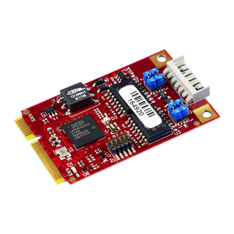
VersaLogic STD32 VL-1225 User manual

-~
ARTISAN
®
~I
TECHNOLOGY
GROUP
Your definitive source
for
quality
pre-owned
equipment.
Artisan Technology
Group
Full-service,
independent
repair
center
with
experienced
engineers
and
technicians
on staff.
We
buy
your
excess,
underutilized,
and
idle
equipment
along
with
credit
for
buybacks
and
trade-ins
.
Custom
engineering
so
your
equipment
works
exactly as
you
specify.
•
Critical
and
expedited
services
•
Leasing
/
Rentals/
Demos
• In
stock/
Ready-to-ship
•
!TAR-certified
secure
asset
solutions
Expert
team
ITrust
guarantee
I
100%
satisfaction
All
tr
ademarks,
br
a
nd
names, a
nd
br
a
nd
s a
pp
earing here
in
are
th
e property of
th
e
ir
r
es
pecti
ve
ow
ner
s.
Find the Versalogic VL1225 at our website: Click HERE

Model VL-1225 & VL-1226
Analog Input/Output Cards for the STD Bus
REFERENCE MANUAL
Contents Copyright 2002
All Rights Reserved
VersaLogic Corporation
3888 Steward Rd.
Eugene, OR 97402
(541) 485-8575
Fax (541) 485-5712
TM
Doc. Rev. 10/30/02
NOTICE:
Although every effort has been made to ensure this documentation is error-free, VersaLogic makes no
representations or warranties with respect to this product and specifically disclaims any implied
warranties of merchantability or fitness for any particular purpose.
VersaLogic reserves the right to revise this product and associated documentation at any time without
obligation to notify anyone of such changes.

ii VL-1225/6 Analog Input/Output Board

VL-1225/6 Analog Input/Output Board iii
Table of Contents
1. Overview
Introduction . . . . . . . . . . . . . . . . . . . . . . . . . . . . . . . . . . . . . . . . . . . . . . . . . . . . . . . . . . . . . . . . . 1-1
Features . . . . . . . . . . . . . . . . . . . . . . . . . . . . . . . . . . . . . . . . . . . . . . . . . . . . . . . . . . . . . . . . . . . . 1-1
Specifications . . . . . . . . . . . . . . . . . . . . . . . . . . . . . . . . . . . . . . . . . . . . . . . . . . . . . . . . . . . . . . . . 1-2
2. Configuration
Jumper Options . . . . . . . . . . . . . . . . . . . . . . . . . . . . . . . . . . . . . . . . . . . . . . . . . . . . . . . . . . . . . . 2-1
VL-1225 Jumper Block Locations . . . . . . . . . . . . . . . . . . . . . . . . . . . . . . . . . . . . . . . . . . . . . 2-2
VL-1225 Jumper Options. . . . . . . . . . . . . . . . . . . . . . . . . . . . . . . . . . . . . . . . . . . . . . . . . . . . 2-3
VL-1226 Jumper Block Locations . . . . . . . . . . . . . . . . . . . . . . . . . . . . . . . . . . . . . . . . . . . . . 2-4
VL-1226 Jumper Options. . . . . . . . . . . . . . . . . . . . . . . . . . . . . . . . . . . . . . . . . . . . . . . . . . . . 2-5
Board Addressing . . . . . . . . . . . . . . . . . . . . . . . . . . . . . . . . . . . . . . . . . . . . . . . . . . . . . . . . . . . . . 2-6
8-Bit I/O Addressing . . . . . . . . . . . . . . . . . . . . . . . . . . . . . . . . . . . . . . . . . . . . . . . . . . . . . . . 2-7
10-Bit I/O Addressing . . . . . . . . . . . . . . . . . . . . . . . . . . . . . . . . . . . . . . . . . . . . . . . . . . . . . . 2-8
16-Bit I/O Addressing . . . . . . . . . . . . . . . . . . . . . . . . . . . . . . . . . . . . . . . . . . . . . . . . . . . . . . 2-9
IOEXP Signal . . . . . . . . . . . . . . . . . . . . . . . . . . . . . . . . . . . . . . . . . . . . . . . . . . . . . . . . . . . . . 2-10
16-Bit Memory Addressing . . . . . . . . . . . . . . . . . . . . . . . . . . . . . . . . . . . . . . . . . . . . . . . . . . 2-11
MEMEX Signal . . . . . . . . . . . . . . . . . . . . . . . . . . . . . . . . . . . . . . . . . . . . . . . . . . . . . . . . . . . 2-12
Analog Input Configuration . . . . . . . . . . . . . . . . . . . . . . . . . . . . . . . . . . . . . . . . . . . . . . . . . . . . . 2-13
Input Mode. . . . . . . . . . . . . . . . . . . . . . . . . . . . . . . . . . . . . . . . . . . . . . . . . . . . . . . . . . . . . . . 2-13
Single Ended Mode . . . . . . . . . . . . . . . . . . . . . . . . . . . . . . . . . . . . . . . . . . . . . . . . . . . . . 2-13
Pseudo-Differential Mode . . . . . . . . . . . . . . . . . . . . . . . . . . . . . . . . . . . . . . . . . . . . . . . . 2-14
Differential Mode . . . . . . . . . . . . . . . . . . . . . . . . . . . . . . . . . . . . . . . . . . . . . . . . . . . . . . 2-14
Current Loop Mode . . . . . . . . . . . . . . . . . . . . . . . . . . . . . . . . . . . . . . . . . . . . . . . . . . . . . 2-15
Input Voltage Range . . . . . . . . . . . . . . . . . . . . . . . . . . . . . . . . . . . . . . . . . . . . . . . . . . . . . . . 2-16
Input Resolution . . . . . . . . . . . . . . . . . . . . . . . . . . . . . . . . . . . . . . . . . . . . . . . . . . . . . . . . . . 2-16
Input Data Format . . . . . . . . . . . . . . . . . . . . . . . . . . . . . . . . . . . . . . . . . . . . . . . . . . . . . . . . 2-17
Analog Output Configuration . . . . . . . . . . . . . . . . . . . . . . . . . . . . . . . . . . . . . . . . . . . . . . . . . . . 2-18
Output Voltage Range . . . . . . . . . . . . . . . . . . . . . . . . . . . . . . . . . . . . . . . . . . . . . . . . . . . . . . 2-18
Output Data Format . . . . . . . . . . . . . . . . . . . . . . . . . . . . . . . . . . . . . . . . . . . . . . . . . . . . . . . 2-19
Output Power-Up Voltage . . . . . . . . . . . . . . . . . . . . . . . . . . . . . . . . . . . . . . . . . . . . . . . . . . . 2-20
Interrupt Configuration . . . . . . . . . . . . . . . . . . . . . . . . . . . . . . . . . . . . . . . . . . . . . . . . . . . . . . . . 2-21
3. Installation
Handling . . . . . . . . . . . . . . . . . . . . . . . . . . . . . . . . . . . . . . . . . . . . . . . . . . . . . . . . . . . . . . . . . . . . 3-1
Installation . . . . . . . . . . . . . . . . . . . . . . . . . . . . . . . . . . . . . . . . . . . . . . . . . . . . . . . . . . . . . . . . . . 3-1
Priority Chain . . . . . . . . . . . . . . . . . . . . . . . . . . . . . . . . . . . . . . . . . . . . . . . . . . . . . . . . . . . . . . . 3-1
Signal Levels . . . . . . . . . . . . . . . . . . . . . . . . . . . . . . . . . . . . . . . . . . . . . . . . . . . . . . . . . . . . . . . . 3-1
External Connections . . . . . . . . . . . . . . . . . . . . . . . . . . . . . . . . . . . . . . . . . . . . . . . . . . . . . . . . . 3-2
Mating Connectors . . . . . . . . . . . . . . . . . . . . . . . . . . . . . . . . . . . . . . . . . . . . . . . . . . . . . . . . 3-2
Physical Pin Locations . . . . . . . . . . . . . . . . . . . . . . . . . . . . . . . . . . . . . . . . . . . . . . . . . . . . . 3-2
Connector Pinout . . . . . . . . . . . . . . . . . . . . . . . . . . . . . . . . . . . . . . . . . . . . . . . . . . . . . . . . . 3-3
Table of Contents

iv VL-1225/6 Analog Input/Output Board
4. Registers
Introduction . . . . . . . . . . . . . . . . . . . . . . . . . . . . . . . . . . . . . . . . . . . . . . . . . . . . . . . . . . . . . . . . . 4-1
Register Mapping . . . . . . . . . . . . . . . . . . . . . . . . . . . . . . . . . . . . . . . . . . . . . . . . . . . . . . . . . . . . . 4-1
Analog Input Registers . . . . . . . . . . . . . . . . . . . . . . . . . . . . . . . . . . . . . . . . . . . . . . . . . . . . . . . . 4-2
Input Channel Select Register . . . . . . . . . . . . . . . . . . . . . . . . . . . . . . . . . . . . . . . . . . . . . . . 4-2
Input Data Low Register . . . . . . . . . . . . . . . . . . . . . . . . . . . . . . . . . . . . . . . . . . . . . . . . . . . . 4-3
Input Data High Register . . . . . . . . . . . . . . . . . . . . . . . . . . . . . . . . . . . . . . . . . . . . . . . . . . . 4-3
Input Data Representation . . . . . . . . . . . . . . . . . . . . . . . . . . . . . . . . . . . . . . . . . . . . . . . . . . 4-4
Input Binary Format (10-Bit Resolution) . . . . . . . . . . . . . . . . . . . . . . . . . . . . . . . . . . . . 4-4
Input Binary Format (11-Bit Resolution) . . . . . . . . . . . . . . . . . . . . . . . . . . . . . . . . . . . . 4-5
Input Offset Binary Format (10-Bit Resolution) . . . . . . . . . . . . . . . . . . . . . . . . . . . . . . . 4-6
Input Offset Binary Format (11-Bit Resolution) . . . . . . . . . . . . . . . . . . . . . . . . . . . . . . . 4-7
Input Two’s Complement Format (10-Bit Resolution) . . . . . . . . . . . . . . . . . . . . . . . . . . 4-8
Input Two’s Complement Format (11-Bit Resolution) . . . . . . . . . . . . . . . . . . . . . . . . . . 4-9
Analog Output Registers . . . . . . . . . . . . . . . . . . . . . . . . . . . . . . . . . . . . . . . . . . . . . . . . . . . . . . . 4-10
Output Data Registers. . . . . . . . . . . . . . . . . . . . . . . . . . . . . . . . . . . . . . . . . . . . . . . . . . . . . . 4-10
Output Data Representation . . . . . . . . . . . . . . . . . . . . . . . . . . . . . . . . . . . . . . . . . . . . . . . . . 4-10
Output Binary Format . . . . . . . . . . . . . . . . . . . . . . . . . . . . . . . . . . . . . . . . . . . . . . . . . . 4-10
Output Offset Binary Format . . . . . . . . . . . . . . . . . . . . . . . . . . . . . . . . . . . . . . . . . . . . . 4-11
Output Two’s Complement Format . . . . . . . . . . . . . . . . . . . . . . . . . . . . . . . . . . . . . . . . 4-12
Interrupt Registers . . . . . . . . . . . . . . . . . . . . . . . . . . . . . . . . . . . . . . . . . . . . . . . . . . . . . . . . . . . 4-13
Interrupt Control Register . . . . . . . . . . . . . . . . . . . . . . . . . . . . . . . . . . . . . . . . . . . . . . . 4-13
Interrupt Status Register . . . . . . . . . . . . . . . . . . . . . . . . . . . . . . . . . . . . . . . . . . . . . . . . 4-13
5. Operation
Polled Mode Analog Input . . . . . . . . . . . . . . . . . . . . . . . . . . . . . . . . . . . . . . . . . . . . . . . . . . . . . . 5-1
Interrupt Mode Analog Input . . . . . . . . . . . . . . . . . . . . . . . . . . . . . . . . . . . . . . . . . . . . . . . . . . . 5-2
Analog Output . . . . . . . . . . . . . . . . . . . . . . . . . . . . . . . . . . . . . . . . . . . . . . . . . . . . . . . . . . . . . . . 5-2
6. Software Examples
Polled Mode Analog Input . . . . . . . . . . . . . . . . . . . . . . . . . . . . . . . . . . . . . . . . . . . . . . . . . . . . . . 6-1
Interrupt Mode Analog Input . . . . . . . . . . . . . . . . . . . . . . . . . . . . . . . . . . . . . . . . . . . . . . . . . . . 6-2
Analog Output . . . . . . . . . . . . . . . . . . . . . . . . . . . . . . . . . . . . . . . . . . . . . . . . . . . . . . . . . . . . . . . 6-5
7. Reference
Specifications . . . . . . . . . . . . . . . . . . . . . . . . . . . . . . . . . . . . . . . . . . . . . . . . . . . . . . . . . . . . . . . . 7-1
VL-1225 Jumper Block Locations . . . . . . . . . . . . . . . . . . . . . . . . . . . . . . . . . . . . . . . . . . . . . . . . 7-2
VL-1226 Jumper Block Locations . . . . . . . . . . . . . . . . . . . . . . . . . . . . . . . . . . . . . . . . . . . . . . . . 7-4
Register Map . . . . . . . . . . . . . . . . . . . . . . . . . . . . . . . . . . . . . . . . . . . . . . . . . . . . . . . . . . . . . . . . 7-6
Calibration . . . . . . . . . . . . . . . . . . . . . . . . . . . . . . . . . . . . . . . . . . . . . . . . . . . . . . . . . . . . . . . . . . 7-7
Input Calibration (VL-1225 and VL-1226) . . . . . . . . . . . . . . . . . . . . . . . . . . . . . . . . . . . . . . . 7-7
Output Calibration (VL-1225 only) . . . . . . . . . . . . . . . . . . . . . . . . . . . . . . . . . . . . . . . . . . . . 7-8
External Connections . . . . . . . . . . . . . . . . . . . . . . . . . . . . . . . . . . . . . . . . . . . . . . . . . . . . . . . . . 7-8
Mating Connectors . . . . . . . . . . . . . . . . . . . . . . . . . . . . . . . . . . . . . . . . . . . . . . . . . . . . . . . . 7-8
Physical Pin Locations . . . . . . . . . . . . . . . . . . . . . . . . . . . . . . . . . . . . . . . . . . . . . . . . . . . . . 7-9
Connector Pinout . . . . . . . . . . . . . . . . . . . . . . . . . . . . . . . . . . . . . . . . . . . . . . . . . . . . . . . . . 7-9
Decimal / Hex / ASCII Conversion Chart . . . . . . . . . . . . . . . . . . . . . . . . . . . . . . . . . . . . . . . . . . 7-10
STD 80 Bus Pinout . . . . . . . . . . . . . . . . . . . . . . . . . . . . . . . . . . . . . . . . . . . . . . . . . . . . . . . . . . . 7-11
STD 32 Bus Pinout Extension . . . . . . . . . . . . . . . . . . . . . . . . . . . . . . . . . . . . . . . . . . . . . . . . . . . 7-12
VL-1225 Parts Placement Diagram . . . . . . . . . . . . . . . . . . . . . . . . . . . . . . . . . . . . . . . . . . . . . . . 7-13
VL-1225 Schematic . . . . . . . . . . . . . . . . . . . . . . . . . . . . . . . . . . . . . . . . . . . . . . . . . . . . . . . . . . . 7-14
VL-1225 Parts List . . . . . . . . . . . . . . . . . . . . . . . . . . . . . . . . . . . . . . . . . . . . . . . . . . . . . . . . . . . . 7-17
VL-1226 Parts Placement Diagram . . . . . . . . . . . . . . . . . . . . . . . . . . . . . . . . . . . . . . . . . . . . . . . 7-19
VL-1226 Schematic . . . . . . . . . . . . . . . . . . . . . . . . . . . . . . . . . . . . . . . . . . . . . . . . . . . . . . . . . . . 7-20
VL-1226 Parts List . . . . . . . . . . . . . . . . . . . . . . . . . . . . . . . . . . . . . . . . . . . . . . . . . . . . . . . . . . . . 7-23
Table of Contents

VL-1225/6 Analog Input/Output Board 1-1
Overview
This manual details the installation and operation of VersaLogic’s VL-1225 and VL-1226 analog I/O cards.
The VL-1225 card includes both analog input and output channels. The VL-1226 includes the same analog
input channels, but no output channels. Both cards provide 10- or 11-bit input resolution.
Introduction
In its standard configuration the VL-1225/6 provides 16 single-ended, or 8 differential analog input
channels. It features 10- or 11-bit resolution, 25 µs conversion time, and an on-board DC to DC converter
(requires +5 volt supply only). The board operates with an input range 0 to +10, ±5, or ±10 volts. It can
accommodate input signals in a single-ended, differential, or pseudo-differential configuration.
Each input channel can be read as desired by the system CPU. The board is capable of 25,000 samples
per second throughput.
In addition to the input channels noted above, the VL-1225 card includes two 8-bit analog output channels.
These channels may be jumpered for 0 to +10, ±5, or ±10 volt output at 5 mA.
The VL-1225 and VL-1226 are plug-in compatible with the Analog Devices RTI-1225 and RTI-1226 cards.
Features
• 16 single-ended or 8 differential input channels.
• Two output channels (VL-1225 only).
• 10-bit (1024 counts), or 11-bit (2048 counts) input resolution.
• 8-bit output resolution (VL-1225 only).
• 25 µs input conversion time.
• 0 to +10, ±5, or ±10 volt input and output ranges.
• 16-bit memory or I/O addressing.
• MEMEX and IOEXP supported.
• +5 volt single supply operation.
• Plug-in replacement for Analog Devices RTI-1225/1226.
Overview

1-2 VL-1225/6 Analog Input/Output Board
Specifications
Specifications are typical at 25°C with 5.0V supply unless otherwise noted.
ANALOG INPUT (VL-1225 and VL-1226)
Number of Channels: 16 single-ended or 8 differential
Range: 0 to +10V, ±5V, ±10V
Resolution:
10 bits (1024 counts) RTI-1225/6 Compatible Mode
11 bits (2048 counts) VL-1225/6 Extended Mode
Conversion Time: 25 µs + settling time
Settling Time: 15 µs
Throughput: 25,000 channels/sec
Overvoltage Protection:
±35V with power on
±20V with power off
Impedance: 1 x 10⁸ Wmin.
Data Format: Binary, offset binary, or two’s complement
Common Mode Voltage (CMV): ±10V min
Common Mode Rejection (CMR): 60 dB
Linearity: ±½ LSB
Differential Nonlinearity: ±½ LSB
Temperature Coefficient:
Gain ±50 ppm/°C of FSR
Offset ±25 ppm/°C of FSR
Addressing: 16 bits + MEMEX or IOEXP
Mapping: 8-byte memory or I/O block on any 8-byte boundary
Size: Meets all STD 32 Bus mechanical specifications
Storage Temperature: -40° to +75 °C
Free Air Operating Temperature: 0° to +65 °C
Power Requirements:
5V ±5% @ 480 ma typ. (VL-1225)
5V ±5% @ 430 ma typ. (VL-1226)
ANALOG OUTPUT (VL-1225 only)
Number of Channels: 2
Resolution: 8 bits (256 counts)
Data Format: Binary, offset binary, or two’s complement
Range: 0 to +10V, ±5V, ±10V
Settling Time: 25 µs (to ±½ LSB)
Linearity: ±½ LSB
Differential Nonlinearity: ±½ LSB
Temperature Coefficient:
Gain ±50 ppm/°C of FSR
Offset ±30 µV/°C
BUS COMPATIBILITY (VL-1225 and VL1226)
STD 80: Full compliance, all bus speeds
STD Z80: Full compliance, all bus speeds
STD 32: I/O slave, SA8-I, IXP
Overview – Specifications

VL-1225/6 Analog Input/Output Board 2-1
Configuration
Configuration
Jumper Options
Various options available on the VL-1225/6 cards are selected using removable jumper blocks (shorting
plugs). Features are selected or deselected by installing or removing the jumpers as noted. The terms
“In” or “Jumpered” are used to indicate an installed plug: “Out” or “Open” are used to indicate a removed
plug.
Figure 2-1 shows the jumper block locations on the VL-1225 card. Figure 2-3 shows the jumper block
locations on the VL-1226 card. The figures indicate the position of the jumpers as shipped from the factory.

2-2 VL-1225/6 Analog Input/Output Board
VL-1225 Jumper Block Locations
Figure 2-1. Jumper Block Locations for VL-1225
Configuration – Jumper Options

VL-1225/6 Analog Input/Output Board 2-3
VL-1225 Jumper Options
JumperJumper
JumperJumper
Jumper AsAs
AsAs
As
BlockBlock
BlockBlock
Block DescriptionDescription
DescriptionDescription
Description ShippedShipped
ShippedShipped
Shipped PagePage
PagePage
Page
V1 Channel 0 Output Voltage Range (see also V16) . . . . . . . . . . . . . . . . . . . . . . . . . . . . . . . . . . . . . . . . . . . . . . . . . . ±10V 2-18
V11-3 = In, V12-4 = In – ±5V
V11-3 = In, V12-4 = Out – ±10V
V11-3 = Out, V12-4 = In – 0 to 10V
V2 Channel 1 Output Voltage Range (see also V16) . . . . . . . . . . . . . . . . . . . . . . . . . . . . . . . . . . . . . . . . . . . . . . . . . . ±10V 2-18
V21-3 = In, V22-4 = In – ±5V
V21-3 = In, V22-4 = Out – ±10V
V21-3 = Out, V22-4 = In – 0 to 10V
V3 Input Voltage Range Select . . . . . . . . . . . . . . . . . . . . . . . . . . . . . . . . . . . . . . . . . . . . . . . . . . . . . . . . . . . . . . . . . . . ±10V 2-16
V31-3 = In, V32-4 = Out, V35-7 = Out, V36-8 = In – ±5V
V31-3 = In, V32-4 = Out, V35-7 = In, V36-8 = Out – ±10V
V31-3 = Out, V32-4 = In, V35-7 = Out, V36-8 = In – 0 to 10V
V4 & V6 Input Mode . . . . . . . . . . . . . . . . . . . . . . . . . . . . . . . . . . . . . . . . . . . . . . . . . . . . . . . . . . . . . . . . . . . . . . . . . . . . . . . S.E. 2-13
V41-2 = In, V43-4 = Out, V45-6 = Out, V47-8 = In, V61-2 = In, V63-4 = Out – Single Ended
V41-2 = In, V43-4 = Out, V45-6 = In, V47-8 = Out, V61-2 = In, V63-4 = Out – Pseudo-Differential
V41-2 = Out, V43-4 = In, V45-6 = Out, V47-8 = Out, V61-2 = Out, V63-4 = In – Differential
V5 Input Data Format . . . . . . . . . . . . . . . . . . . . . . . . . . . . . . . . . . . . . . . . . . . . . . . . . . . . . . . . . . . . . . . . . . . . . . . . . . 2’s Comp. 2-17
V51-3 = Out, V52-4 = In – Binary / Offset Binary
V51-3 = In, V52-4 = Out – Two’s Complement
V71-3 & 3-5 Channel 0 Output Data Format . . . . . . . . . . . . . . . . . . . . . . . . . . . . . . . . . . . . . . . . . . . . . . . . . . . . . . . . . . . . . . . . 2’s Comp. 2-19
V71-3 = In, V73-5 = Out – Binary / Offset Binary
V71-3 = Out, V73-5 = In – Two’s Complement
V72-4 & 4-6 Channel 1 Output Data Format . . . . . . . . . . . . . . . . . . . . . . . . . . . . . . . . . . . . . . . . . . . . . . . . . . . . . . . . . . . . . . . . 2’s Comp. 2-19
V72-4 = In, V74-6 = Out – Binary / Offset Binary
V72-4 = Out, V74-6 = In – Two’s Complement
V8 MEMEXSelect . . . . . . . . . . . . . . . . . . . . . . . . . . . . . . . . . . . . . . . . . . . . . . . . . . . . . . . . . . . . . . . . . . . . . . . . . . . . . Ignore 2-12
V81-2 = In, V82-3 = Out – Ignore MEMEX
V81-2 = Out, V82-3 = Out – Enable on MEMEX high
V81-2 = Out, V82-3 = In – Enable on MEMEX low
V9 Board Address (A10 – A15) . . . . . . . . . . . . . . . . . . . . . . . . . . . . . . . . . . . . . . . . . . . . . . . . . . . . . . . . . . . . . . . . . . . FF08H 2-6
V91-2 = In – A15 decoded Low V91-2 = Out – A15 decoded High
V93-4 = In – A14 decoded Low V93-4 = Out – A14 decoded High
V95-6 = In – A13 decoded Low V95-6 = Out – A13 decoded High
V97-8 = In – A12 decoded Low V97-8 = Out – A12 decoded High
V99-10 = In – A11 decoded Low V99-10 = Out – A11 decoded High
V911-12 = In – A10 decoded Low V911-12 = Out – A10 decoded High
V10 IOEXP Select . . . . . . . . . . . . . . . . . . . . . . . . . . . . . . . . . . . . . . . . . . . . . . . . . . . . . . . . . . . . . . . . . . . . . . . . . . . . . Ignore 2-10
V101-2 = In, V102-3 = Out – Ignore IOEXP
V101-2 = Out, V102-3 = Out – Enable on IOEXP high
V101-2 = Out, V102-3 = In – Enable on IOEXP low
V11 Board Address (A8, A9) / 8-Bit Mode Selector . . . . . . . . . . . . . . . . . . . . . . . . . . . . . . . . . . . . . . . . . . . . . . . . . . . . A8Hi, A9Hi 2-6
V111-3 = In, V112-4 = In, V113-5 = Out, V114-6 = Out – 8-Bit Mode (ignore A8 & A9)
V111-3 = Out, V112-4 = Out, V113-5 = Out, V114-6 = Out – 10- or 16-Bit Decoding (A8 = High, A9 = High)
V111-3 = Out, V112-4 = Out, V113-5 = Out, V114-6 = In – 10- or 16-Bit Decoding (A8 = High, A9 = Low)
V111-3 = Out, V112-4 = Out, V113-5 = In, V114-6 = Out – 10- or 16-Bit Decoding (A8 = Low, A9 = High)
V111-3 = Out, V112-4 = Out, V113-5 = In, V114-6 = In – 10- or 16-Bit Decoding (A8 = Low, A9 = Low)
V12 Board Address (A3 – A7) . . . . . . . . . . . . . . . . . . . . . . . . . . . . . . . . . . . . . . . . . . . . . . . . . . . . . . . . . . . . . . . . . . . . FF08H 2-6
V121-2 = In – A7 decoded Low V121-2 = Out – A7 decoded High
V123-4 = In – A6 decoded Low V123-4 = Out – A6 decoded High
V125-6 = In – A5 decoded Low V125-6 = Out – A5 decoded High
V127-8 = In – A4 decoded Low V127-8 = Out – A4 decoded High
V129-10 = In – A3 decoded Low V129-10 = Out – A3 decoded High
V13 Address Type Select . . . . . . . . . . . . . . . . . . . . . . . . . . . . . . . . . . . . . . . . . . . . . . . . . . . . . . . . . . . . . . . . . . . . . . . . Memory 2-6
V131-2 = In, V133-4 = Out, V135-6 = Out, V137-8 = In – 16-Bit Memory Mapped
V131-2 = In, V133-4 = Out, V135-6 = In, V137-8 = Out – 8- or 10-Bit I/O Mapped
V131-2 = Out, V133-4 = In, V135-6 = Out, V137-8 = In – 16-Bit I/O Mapped
V14 Analog Input Resolution . . . . . . . . . . . . . . . . . . . . . . . . . . . . . . . . . . . . . . . . . . . . . . . . . . . . . . . . . . . . . . . . . . . . . 10-Bit 2-16
V14 = In – 10-Bit V14 = Out – 11-Bit
V15 Interrupt Request Select . . . . . . . . . . . . . . . . . . . . . . . . . . . . . . . . . . . . . . . . . . . . . . . . . . . . . . . . . . . . . . . . . . . . . None 2-21
V151-2 = Out, V153-4 = Out, V155-6 = Out, V157-8 = Out – None
V151-2 = Out, V153-4 = Out, V155-6 = Out, V157-8 = In – INT2* (P50)
V151-2 = Out, V153-4 = Out, V155-6 = In, V157-8 = Out – INT1* (P37)
V151-2 = Out, V153-4 = In, V155-6 = Out, V157-8 = Out – INT* (P44)
V151-2 = In, V153-4 = Out, V155-6 = Out, V157-8 = Out – IRQx (E47)
V16 D/A Power-Up Output Voltage . . . . . . . . . . . . . . . . . . . . . . . . . . . . . . . . . . . . . . . . . . . . . . . . . . . . . . . . . . . . . . . . . RTI-1225 2-20
V161-2 = In, V162-3 = Out – Zero Volts (in Two’s Complement/Bipolar, and Binary/Unipolar modes)
– Negative Full Scale (in Offset Binary/Bipolar mode)
V161-2 = Out, V162-3 = In – Zero Volts (in Offset Binary/Bipolar mode)
– Negative Full Scale (in Two’s Complement/Bipolar mode)
– Half Scale (in Binary/Unipolar mode)
Figure 2-2. VL-1225 Jumper Functions
Configuration – Jumper Options
2-4 VL-1225/6 Analog Input/Output Board
VL-1226 Jumper Block Locations
Figure 2-3. Jumper Block Locations for VL-1226
Configuration – Jumper Options

VL-1225/6 Analog Input/Output Board 2-5
VL-1226 Jumper Options
JumperJumper
JumperJumper
Jumper AsAs
AsAs
As
BlockBlock
BlockBlock
Block DescriptionDescription
DescriptionDescription
Description ShippedShipped
ShippedShipped
Shipped PagePage
PagePage
Page
V1 1225 Only . . . . . . . . . . . . . . . . . . . . . . . . . . . . . . . . . . . . . . . . . . . . . . . . . . . . . . . . . . . . . . . . . . . . . . . . . . . . . . . . — —
V2 1225 Only . . . . . . . . . . . . . . . . . . . . . . . . . . . . . . . . . . . . . . . . . . . . . . . . . . . . . . . . . . . . . . . . . . . . . . . . . . . . . . . . — —
V3 Input Voltage Range Select . . . . . . . . . . . . . . . . . . . . . . . . . . . . . . . . . . . . . . . . . . . . . . . . . . . . . . . . . . . . . . . . . . . ±10V 2-16
V31-3 = In, V32-4 = Out, V35-7 = Out, V36-8 = In – ±5V
V31-3 = In, V32-4 = Out, V35-7 = In, V36-8 = Out – ±10V
V31-3 = Out, V32-4 = In, V35-7 = Out, V36-8 = In – 0 to 10V
V4 & V6 Input Mode . . . . . . . . . . . . . . . . . . . . . . . . . . . . . . . . . . . . . . . . . . . . . . . . . . . . . . . . . . . . . . . . . . . . . . . . . . . . . . . S.E. 2-13
V41-2 = In, V43-4 = Out, V45-6 = Out, V47-8 = In, V61-2 = In, V63-4 = Out – Single Ended
V41-2 = In, V43-4 = Out, V45-6 = In, V47-8 = Out, V61-2 = In, V63-4 = Out – Pseudo-Differential
V41-2 = Out, V43-4 = In, V45-6 = Out, V47-8 = Out, V61-2 = Out, V63-4 = In – Differential
V5 Input Data Format . . . . . . . . . . . . . . . . . . . . . . . . . . . . . . . . . . . . . . . . . . . . . . . . . . . . . . . . . . . . . . . . . . . . . . . . . . 2’s Comp. 2-17
V51-3 = Out, V52-4 = In – Binary / Offset Binary
V51-3 = In, V52-4 = Out – Two’s Complement
V7 1225 Only . . . . . . . . . . . . . . . . . . . . . . . . . . . . . . . . . . . . . . . . . . . . . . . . . . . . . . . . . . . . . . . . . . . . . . . . . . . . . . . . — —
V8 MEMEXSelect . . . . . . . . . . . . . . . . . . . . . . . . . . . . . . . . . . . . . . . . . . . . . . . . . . . . . . . . . . . . . . . . . . . . . . . . . . . . . Ignore 2-12
V81-2 = In, V82-3 = Out – Ignore MEMEX
V81-2 = Out, V82-3 = Out – Enable on MEMEX high
V81-2 = Out, V82-3 = In – Enable on MEMEX low
V9 Board Address (A10 – A15) . . . . . . . . . . . . . . . . . . . . . . . . . . . . . . . . . . . . . . . . . . . . . . . . . . . . . . . . . . . . . . . . . . . FF08H 2-6
V91-2 = In – A15 decoded Low V91-2 = Out – A15 decoded High
V93-4 = In – A14 decoded Low V93-4 = Out – A14 decoded High
V95-6 = In – A13 decoded Low V95-6 = Out – A13 decoded High
V97-8 = In – A12 decoded Low V97-8 = Out – A12 decoded High
V99-10 = In – A11 decoded Low V99-10 = Out – A11 decoded High
V911-12 = In – A10 decoded Low V911-12 = Out – A10 decoded High
V10 IOEXP Select . . . . . . . . . . . . . . . . . . . . . . . . . . . . . . . . . . . . . . . . . . . . . . . . . . . . . . . . . . . . . . . . . . . . . . . . . . . . . Ignore 2-10
V101-2 = In, V102-3 = Out – Ignore IOEXP
V101-2 = Out, V102-3 = Out – Enable on IOEXP high
V101-2 = Out, V102-3 = In – Enable on IOEXP low
V11 Board Address (A8, A9) / 8-Bit Mode Selector . . . . . . . . . . . . . . . . . . . . . . . . . . . . . . . . . . . . . . . . . . . . . . . . . . . . A8Hi, A9Hi 2-6
V111-3 = In, V112-4 = In, V113-5 = Out, V114-6 = Out – 8-Bit Mode (ignore A8 & A9)
V111-3 = Out, V112-4 = Out, V113-5 = Out, V114-6 = Out – 10- or 16-Bit Decoding (A8 = High, A9 = High)
V111-3 = Out, V112-4 = Out, V113-5 = Out, V114-6 = In – 10- or 16-Bit Decoding (A8 = High, A9 = Low)
V111-3 = Out, V112-4 = Out, V113-5 = In, V114-6 = Out – 10- or 16-Bit Decoding (A8 = Low, A9 = High)
V111-3 = Out, V112-4 = Out, V113-5 = In, V114-6 = In – 10- or 16-Bit Decoding (A8 = Low, A9 = Low)
V12 Board Address (A3 – A7) . . . . . . . . . . . . . . . . . . . . . . . . . . . . . . . . . . . . . . . . . . . . . . . . . . . . . . . . . . . . . . . . . . . . FF08H 2-6
V111-2 = In – A7 decoded Low V111-2 = Out – A7 decoded High
V113-4 = In – A6 decoded Low V113-4 = Out – A6 decoded High
V115-6 = In – A5 decoded Low V115-6 = Out – A5 decoded High
V117-8 = In – A4 decoded Low V117-8 = Out – A4 decoded High
V119-10 = In – A3 decoded Low V119-10 = Out – A3 decoded High
V13 Address Type Select . . . . . . . . . . . . . . . . . . . . . . . . . . . . . . . . . . . . . . . . . . . . . . . . . . . . . . . . . . . . . . . . . . . . . . . . Memory 2-6
V131-2 = In, V133-4 = Out, V135-6 = Out, V137-8 = In – 16-Bit Memory Mapped
V131-2 = In, V133-4 = Out, V135-6 = In, V137-8 = Out – 8- or 10-Bit I/O Mapped
V131-2 = Out, V133-4 = In, V135-6 = Out, V137-8 = In – 16-Bit I/O Mapped
V14 Analog Input Resolution . . . . . . . . . . . . . . . . . . . . . . . . . . . . . . . . . . . . . . . . . . . . . . . . . . . . . . . . . . . . . . . . . . . . . 10-Bit 2-16
V14 = In – 10-Bit V14 = Out – 11-Bit
V15 Interrupt Request Select . . . . . . . . . . . . . . . . . . . . . . . . . . . . . . . . . . . . . . . . . . . . . . . . . . . . . . . . . . . . . . . . . . . . . None 2-21
V151-2 = Out, V153-4 = Out, V155-6 = Out, V157-8 = Out – None
V151-2 = Out, V153-4 = Out, V155-6 = Out, V157-8 = In – INT2* (P50)
V151-2 = Out, V153-4 = Out, V155-6 = In, V157-8 = Out – INT1* (P37)
V151-2 = Out, V153-4 = In, V155-6 = Out, V157-8 = Out – INT* (P44)
V151-2 = In, V153-4 = Out, V155-6 = Out, V157-8 = Out – IRQx (E47)
V16 1225 Only . . . . . . . . . . . . . . . . . . . . . . . . . . . . . . . . . . . . . . . . . . . . . . . . . . . . . . . . . . . . . . . . . . . . . . . . . . . . . . . . — —
Figure 2-4. VL-1226 Jumper Functions
Configuration – Jumper Options
2-6 VL-1225/6 Analog Input/Output Board
Board Addressing
The VL-1225/6 supports 8-, 10-, and 16-bit I/O addressing, and 16-bit memory addressing. 8-bit I/O
addressing is used with most 8-bit processors (Z80, 8085, 6809, etc.) which provide 256 I/O addresses. 10-
or 16-bit addressing can be used with 16-bit processors (8088, 80188, 80186, etc.) to decode 1024 or 65536
I/O port addresses. 16-bit memory addressing can be used with most 8-bit processors (Z80, 8085, 6809,
etc.) if desired.
I/O addressing can be extended (capacity doubled) using the IOEXP signal which is decoded by the VL-1225/
6. Memory addressing can be extended (capacity doubled) using the MEMEX signal which is decoded by
the VL-1225/6.
As shipped the board is configured for 16-bit memory addressing with a board address of hex FF08. The
card occupies eight consecutive addresses (i.e. FF08H to FF0FH). The VL-1226 uses four of these
addresses as control, data, and status registers, the remaining four are inaccessible. The VL-1225 uses
six addresses, with two inaccessible. See the Register Mapping section on page 4-1 for further information.
Configuration – Board Addressing

VL-1225/6 Analog Input/Output Board 2-7
8-Bit I/O Addressing
To configure the board for an 8-bit I/O address refer to the figure below. Use the table to select the
jumpering for the appropriate upper and lower halves of the desired starting address (i.e., “3” and “0” =
hex address 30).
This jumper configuration ignores the state of the IOEXP signal in addressing the board. To use the
IOEXP signal refer to page 2-10.
Upper Lower
V121-2 V123-4 V125-6 V127-8 Digit V129-10 Digit
XXXX0 X0
XXX–1 – 8
XX–X2
XX––3
X–XX4
X–X– 5
X––X6
X–––7
–XXX8
–XX– 9
–X–XA
–X––B
–– XXC
––X–D
–––XE
––––F
X = Jumper installed
– = Jumper removed
JumperJumper
JumperJumper
Jumper AsAs
AsAs
As
BlockBlock
BlockBlock
Block DescriptionDescription
DescriptionDescription
Description ShippedShipped
ShippedShipped
Shipped
V8 MEMEX Select . . . . . . . . . . . . . . . . . . . . . . . . . . . . . . . . . . . . . . . . . . . . . . . . . . . . . . . . . . . . . . . . . . . Ignore
V9 Board Address (A10 – A15) . . . . . . . . . . . . . . . . . . . . . . . . . . . . . . . . . . . . . . . . . . . . . . . . . . . . . . . . . FF08H
V10 IOEXP Select . . . . . . . . . . . . . . . . . . . . . . . . . . . . . . . . . . . . . . . . . . . . . . . . . . . . . . . . . . . . . . . . . . . . Ignore
V11 Board Address (A8, A9) / 8-Bit Mode Selector . . . . . . . . . . . . . . . . . . . . . . . . . . . . . . . . . . . . . . . . . . . A8Hi, A9Hi
V12 Board Address (A3 – A7) . . . . . . . . . . . . . . . . . . . . . . . . . . . . . . . . . . . . . . . . . . . . . . . . . . . . . . . . . . . FF08H
V13 Address Type Select . . . . . . . . . . . . . . . . . . . . . . . . . . . . . . . . . . . . . . . . . . . . . . . . . . . . . . . . . . . . . . Memory
Figure 2-5. 8-Bit I/O Address Jumpers
Configuration – Board Addressing

2-8 VL-1225/6 Analog Input/Output Board
10-Bit I/O Addressing
To configure the board for a 10-bit I/O address refer to the figure below. Use the table to select the
jumpering for the appropriate upper, middle, and lower hex digits of the desired starting address (i.e., “1”
and “3” and “0” = hex address 130).
This jumper configuration ignores the state of the IOEXP signal in addressing the board. To use the
IOEXP signal refer to page 2-10.
Upper Middle Lower
V113-5 V114-6 Digit V121-2 V123-4 V125-6 V127-8 Digit V129-10 Digit
XX0 XXXX0 X 0
X–1 XXX– 1 – 8
–X2 XX– X2
––3 XX––3
X–XX4
X–X– 5
X––X6
X–––7
–XXX8
–XX– 9
–X–XA
–X––B
–– XXC
––X–D
–––XE
––––F
X = Jumper installed
– = Jumper removed
JumperJumper
JumperJumper
Jumper AsAs
AsAs
As
BlockBlock
BlockBlock
Block DescriptionDescription
DescriptionDescription
Description ShippedShipped
ShippedShipped
Shipped
V8 MEMEX Select . . . . . . . . . . . . . . . . . . . . . . . . . . . . . . . . . . . . . . . . . . . . . . . . . . . . . . . . . . . . . . . . . . . Ignore
V9 Board Address (A10 – A15) . . . . . . . . . . . . . . . . . . . . . . . . . . . . . . . . . . . . . . . . . . . . . . . . . . . . . . . . . FF08H
V10 IOEXP Select . . . . . . . . . . . . . . . . . . . . . . . . . . . . . . . . . . . . . . . . . . . . . . . . . . . . . . . . . . . . . . . . . . . . Ignore
V11 Board Address (A8, A9) / 8-Bit Mode Selector . . . . . . . . . . . . . . . . . . . . . . . . . . . . . . . . . . . . . . . . . . . A8Hi, A9Hi
V12 Board Address (A3 – A7) . . . . . . . . . . . . . . . . . . . . . . . . . . . . . . . . . . . . . . . . . . . . . . . . . . . . . . . . . . . FF08H
V13 Address Type Select . . . . . . . . . . . . . . . . . . . . . . . . . . . . . . . . . . . . . . . . . . . . . . . . . . . . . . . . . . . . . . Memory
Figure 2-6. 10-Bit I/O Address Jumpers
Configuration – Board Addressing

VL-1225/6 Analog Input/Output Board 2-9
16-Bit I/O Addressing
To configure the board for a 16-bit I/O address refer to the figure below. See the table to select the
jumpering for the appropriate four hex digits of the desired starting address (i.e., “6” and “1” and “3” and
“0” = hex address 6130).
This jumper configuration ignores the state of the IOEXP signal in addressing the board. To use the
IOEXP signal refer to page 2-10.
Upper Second Third Lower
V91-2 V93-4 V95-6 V97-8 Digit V99-10 V911-12 V113-5 V114-6 Digit V121-2 V123-4 V125-6 V127-8 Digit V129-10 Digit
XXXX0 XXXX 0 XXXX 0 X 0
XXX–1 XXX– 1 XXX– 1 – 8
XX–X2 XX– X 2 XX–X 2
XX–– 3 XX–– 3 XX– – 3
X–XX4 X– XX 4 X–XX 4
X–X– 5 X–X– 5 X– X– 5
X––X6 X––X 6 X––X 6
X–––7 X––– 7 X––– 7
–XXX8 – XXX 8 –XXX 8
–XX– 9 –XX– 9 – XX– 9
–X–XA –X–X A –X–X A
–X––B –X–– B –X–– B
––XXC ––XX C ––XX C
––X–D ––X– D ––X– D
–––XE –––X E –––X E
––––F –––– F –––– F
X = Jumper installed
–= Jumper removed
JumperJumper
JumperJumper
Jumper AsAs
AsAs
As
BlockBlock
BlockBlock
Block DescriptionDescription
DescriptionDescription
Description ShippedShipped
ShippedShipped
Shipped
V8 MEMEX Select . . . . . . . . . . . . . . . . . . . . . . . . . . . . . . . . . . . . . . . . . . . . . . . . . . . . . . . . . . . . . . . . . . . Ignore
V9 Board Address (A10 –A15) . . . . . . . . . . . . . . . . . . . . . . . . . . . . . . . . . . . . . . . . . . . . . . . . . . . . . . . . . FF08H
V10 IOEXP Select . . . . . . . . . . . . . . . . . . . . . . . . . . . . . . . . . . . . . . . . . . . . . . . . . . . . . . . . . . . . . . . . . . . . Ignore
V11 Board Address (A8, A9) / 8-Bit Mode Selector . . . . . . . . . . . . . . . . . . . . . . . . . . . . . . . . . . . . . . . . . . . A8Hi, A9Hi
V12 Board Address (A3 –A7) . . . . . . . . . . . . . . . . . . . . . . . . . . . . . . . . . . . . . . . . . . . . . . . . . . . . . . . . . . . FF08H
V13 Address Type Select . . . . . . . . . . . . . . . . . . . . . . . . . . . . . . . . . . . . . . . . . . . . . . . . . . . . . . . . . . . . . . Memory
Figure 2-7. 16-Bit I/O Address Jumpers
Configuration – Board Addressing

2-10 VL-1225/6 Analog Input/Output Board
IOEXP Signal
The IOEXP (I/O expansion) signal on the STD Bus is normally used to select between two different I/O
banks or maps. It can be used to double the number of available I/O addresses in the system (by selecting
between two banks of I/O boards). The IOEXP signal is usually controlled by (or jumpered to ground on)
the system CPU card.
A low IOEXP signal usually selects the standard or normal I/O map. A high IOEXP signal usually selects
the secondary or alternate I/O map. Boards that ignore (or do not decode) IOEXP will appear in both I/
O maps.
As shipped the IOEXP jumper is configured to ignore the IOEXP signal. The board will be addressed
whether the IOEXP signal is high or low. It can be jumpered for two other modes as shown below.
JumperJumper
JumperJumper
Jumper AsAs
AsAs
As
BlockBlock
BlockBlock
Block DescriptionDescription
DescriptionDescription
Description ShippedShipped
ShippedShipped
Shipped
V10 IOEXP Select . . . . . . . . . . . . . . . . . . . . . . . . . . . . . . . . . . . . . . . . . . . . . . . . . . . . . . . . . . . . . . . . . . . . Ignore
V101-2 = In, V102-3 = Out –Ignore IOEXP
V101-2 = Out, V102-3 = Out –Enable on IOEXP high
V101-2 = Out, V102-3 = In –Enable on IOEXP low
Figure 2-8. IOEXP Options
Configuration – Board Addressing

VL-1225/6 Analog Input/Output Board 2-11
16-Bit Memory Addressing
To configure the board for a 16-bit memory address refer to the figure below. Use the table to select the
jumpering for the appropriate four hex digits of the desired starting address (i.e., “6” and “1” and “3” and
“0” = hex address 6130).
This jumper configuration ignores the state of the MEMEX signal in addressing the board. To use the
MEMEX signal refer to the MEMEX Signal heading in this section.
Upper Second Third Lower
V91-2 V93-4 V95-6 V97-8 Digit V99-10 V911-12 V113-5 V114-6 Digit V121-2 V123-4 V125-6 V127-8 Digit V129-10 Digit
XXXX0 XXXX 0 XXXX 0 X 0
XXX–1 XXX–1 XXX–1–8
XX–X2 XX–X2 XX–X2
XX––3 XX–– 3 XX–– 3
X–XX4 X–XX 4 X–XX 4
X–X–5X–X–5X–X–5
X––X6 X––X6 X––X6
X–––7X––– 7X––– 7
–XXX8 –XXX 8 –XXX 8
–XX–9–XX–9–XX–9
–X–XA –X–XA –X–XA
–X––B–X–– B–X–– B
––XXC ––XX C ––XX C
––X–D––X–D––X–D
–––XE –––XE –––XE
––––F–––– F–––– F
X = Jumper installed
–= Jumper removed
JumperJumper
JumperJumper
Jumper AsAs
AsAs
As
BlockBlock
BlockBlock
Block DescriptionDescription
DescriptionDescription
Description ShippedShipped
ShippedShipped
Shipped
V8 MEMEX Select . . . . . . . . . . . . . . . . . . . . . . . . . . . . . . . . . . . . . . . . . . . . . . . . . . . . . . . . . . . . . . . . . . . Ignore
V9 Board Address (A10 –A15) . . . . . . . . . . . . . . . . . . . . . . . . . . . . . . . . . . . . . . . . . . . . . . . . . . . . . . . . . FF08H
V10 IOEXP Select . . . . . . . . . . . . . . . . . . . . . . . . . . . . . . . . . . . . . . . . . . . . . . . . . . . . . . . . . . . . . . . . . . . . Ignore
V11 Board Address (A8, A9) / 8-Bit Mode Selector . . . . . . . . . . . . . . . . . . . . . . . . . . . . . . . . . . . . . . . . . . . A8Hi, A9Hi
V12 Board Address (A3 –A7) . . . . . . . . . . . . . . . . . . . . . . . . . . . . . . . . . . . . . . . . . . . . . . . . . . . . . . . . . . . FF08H
V13 Address Type Select . . . . . . . . . . . . . . . . . . . . . . . . . . . . . . . . . . . . . . . . . . . . . . . . . . . . . . . . . . . . . . Memory
Figure 2-9. 16-Bit Memory Address Jumpers
Configuration – Board Addressing

2-12 VL-1225/6 Analog Input/Output Board
MEMEX Signal
The MEMEX (memory expansion) signal on the STD Bus is normally used to select between two different
memory banks or maps. It can be used to double the number of available memory addresses in the system
(by selecting between the two memory banks). The MEMEX signal is usually controlled by (or jumpered
to ground on) the system CPU card.
A low MEMEX signal usually selects the standard or normal memory map. A high MEMEX signal usually
selects the secondary or alternate memory map. Boards that ignore (or do not decode) MEMEX will appear
in both memory maps.
As shipped the MEMEX jumper is configured to ignore the MEMEX signal. The board will be addressed
whether the MEMEX signal is high or low. It can be jumpered for two other modes as shown below.
JumperJumper
JumperJumper
Jumper AsAs
AsAs
As
BlockBlock
BlockBlock
Block DescriptionDescription
DescriptionDescription
Description ShippedShipped
ShippedShipped
Shipped
V8 MEMEX Select . . . . . . . . . . . . . . . . . . . . . . . . . . . . . . . . . . . . . . . . . . . . . . . . . . . . . . . . . . . . . . . . . . . Ignore
V81-2 = In, V82-3 = Out –Ignore MEMEX
V81-2 = Out, V82-3 = Out –Enable on MEMEX high
V81-2 = Out, V82-3 = In –Enable on MEMEX low
Figure 2-10. MEMEX Options
Configuration – Board Addressing

VL-1225/6 Analog Input/Output Board 2-13
Analog Input Configuration
The VL-1225/6 board accommodates 16 single-ended or 8 differential channels.
Input Mode
The VL-1225/6 board can be configured for three types of voltage inputs: differential, single-ended, and
pseudo-differential. In addition, by adding an external user-supplied 500 Wresistor, the VL-1225/6 can be
hooked up to a 4-20 ma current loop. All inputs connected to the boards must be of the same type.
Typical connections for the three input modes are shown in the figures below. Since ground loops (current
flowing between various equipment ground lines) affect analog measurements made with reference to
ground, careful attention should be paid to the ground connections shown. In particular, the STD Bus
power supply logic ground line should never be connected to earth ground when operating in the
differential or pseudo-differential modes.
Single Ended Mode
The single-ended mode is used for signals that are referenced to a common ground. It is normally used
only for higher level signals on short distance runs (less than 10 feet). In this mode up to 16 input channels
can be accommodated.
Figure 2-11. Single Ended Input Mode
Configuration – Analog Input Configuration
This manual suits for next models
1
Table of contents
Other VersaLogic Control Unit manuals
Popular Control Unit manuals by other brands

Monacor
Monacor ATT-135/SI quick guide

Advantech
Advantech AIW-357 DK-G2U user manual

ProSoft Technology
ProSoft Technology InRax MVI71-DNPSNET user manual

Emerson
Emerson Topworx D Series Installation, operation & maintenance manual

PURGEnVENT
PURGEnVENT 7900AAV manual

Weidmüller
Weidmüller DPA/RTD operating instructions