VICOR PI352 series User manual

UG:307 vicorpower.com Applications Engineering: 800 927.9474 Page 1
PI352x-0x-EVAL1
Cool-Power®ZVS Switching Regulators
60VIN Buck Customer Eval Board User Guide
Note: Acutal evaluation board appearance may vary slightly depending on product ordered
Introduction
This customer evaluation board is designed for the PI352x family of 10 x 14 ZVS Bucks. It
can be configured to demonstrate a single product in a stand-alone local sense or a remote
sense configuration.
The PI352x family of wide input range DC-DC ZVS-Buck regulators feature high efficiency with
integrated controller, power switches, and support components all within a high density 0.4” x
0.55” System-in-Package (SiP). Required components are placed inside a demarcation featuring a
solution size of 7.3” x 1.74”. The demarcation includes an external inductor, compensation capacitor,
voltage selection resistors, soft-start capacitor, and input-output capacitors to form a complete
DC-DC regulator.
Contents Page
USER GUIDE | UG:307
Introduction 1
Box Contents 3
Recommended
Test Equipment 3
Features 3
Board Operation Modes 4
Thermal Consideration 4
Power Up Procedure 4
Board Description 5
General Components 6
Test Points Description 8
Sockets Description 9
Schematic 10
Schematic (Cont.) 11

UG:307 vicorpower.com Applications Engineering: 800 927.9474 Page 2
Bill of Materials
IMPORTANT NOTICE:
Be sure to read the precautions below entirely BEFORE using the Evaluation Board. Do not operate the
evaluation board unless you have the appropriate safety precautions in place on your bench to ensure a
successful experience.
The list below is not comprehensive and is not a substitute for common sense and good practice.
Refer to the specific regulator module data sheet for electrical rating of the device, thermal and
mechanical product details. It is important to remain within the device rated range when testing.
When testing electronic products always use approved safety glasses. Follow good laboratory practice
and procedures.
During operation insure the power devices and surrounding structures can be operated safely.
Care should be taken to protect the user from accidental contact when under power.
Provide a strain relief for wires and place the system on the bench in such a way as to prevent
accidental displacement from bench top.
Review thermal consideration and guideline associated with operating the evaluation board. Most
notably use a bench top fan and use rubber feet to elevate the PCB as they allow air flow to
the bottom.
Remove power and use caution when connecting and disconnecting test probes and interface lines
to avoid inadvertent short circuits and contact with hot surfaces.
Verify power connections to avoid reversing applied voltage polarities.
Avoid creating ground loops between the SGND and PGND pins when making measurements.
The product evaluation board is designed for general laboratory evaluation. It is not recommended
for installation in end user equipment.

UG:307 vicorpower.com Applications Engineering: 800 927.9474 Page 3
The evaluation board is designed to faciliatate the evaluation of the performance of Vicor’s mounted
ZVS buck product. Sockets are provided to permit quick probing. Input sockets can be used to place
a bulk capacitor. The evaluation board provides lugs, and bottom layer banana jack footprint for input
and output connections, signal connectors allowing wire, signal test points for easy connection to
standard test equipment, and Kelvin Johnson-Jack for accurate voltage measurements of power nodes.
Box Contents
The evaluation board ships with the following contents:
1 Customer evaluation board
3 x pre-installed jumpers
1 x hardware kit: 5 x size 10 screws, lugs and washers
Recommended Test Equipment
The following is a list of recommended test equipment.
1. Safety glasses.
2. DC power supply: Refer to the specific PI352x model datasheet to ensure the supply has sufficient
power and current capability.
3. Electronic load: Refer to the specific PI352x model datasheet to ensure the load has sufficient
power handling and current capability for testing.
4. Bench top cooling fan.
5. Digital multi-meters (DMMs).
6. Oscilloscope and probes.
7. Interconnect wires, cables and fastening hardware.
Features
1. Input and output lugs for source and load connections.
2. Input sockets to place through-hole input aluminum-electrolytic capacitor.
3. Input source filter (L102, R105).
4. Toggle switch (S101) for enabling and disabling the regulator through the EN pin.
5. Oscilloscope probe jack for accurate, high frequency input (J101) and output (J102) voltage
measurement.
6. Signal pins test points and wire connectors.
7. Kelvin voltage test points and sockets for all pins of the SiP product.
8. Access to voltage switching node VS1 with a nearby ground receptacle.
9. Mode selection switch for local (default) and remote sense loop.
10. Trim control selection for both local and remote sense:
a. ADJ: potentiometer to exercise the full output range.
b. Fixed: resistor to set unit to nominal output.
11. Local and remote sense AC signal injection (J201).

UG:307 vicorpower.com Applications Engineering: 800 927.9474 Page 4
Board Operation Modes
S101 provides control over enable.
In the “OFF” position, the switch will connect SGND pin to the EN net, which disables the
regulator output.
In the “ON” position, the EN net is allowed to float.
The PI352x evaluation board supports the following operating modes:
Mode S202 S201 S203 J201 (+VRS, -VRS)
Local loop, fixed
Nominal output LS FIXED -Place jumper (J201 pin 1-2) to
short R211 for accurate result -
Local loop, with
Trim range (R206) LS ADJ -
Turn (R206) clockwise to
increase the output voltage and
counterclockwise to decrease the
output voltage.
-
Remote loop,
fixed Nominal
output
-FIXED RS Place jumper (J201 pin 1-2) to
short R211 for accurate result Used to connect to point
of load. If not connected
(R223-R224 = 100Ω) will
be in the loop connecting
this node to local +VOUT
Remote loop, with
Trim range (R221) -ADJ RS
Turn (R206) clockwise to
increase the output voltage and
counterclockwise to decrease the
output voltage.
Thermal Consideration
A fan blowing across the evaluation board is recommended for operation. The fan should be placed
about 4 inches away from the evaluation board edge. A typical bench top fan is recommended
providing about 1000LFM. Using the supplied rubber feet is also required in order to elevate the board
about 0.4 inches off a flat surface and enable air flow underneath the PCB.
Power Up Procedure
1. Confirm bench equipment is powered off.
2. Connect input DC power supply positive lead to +VIN input lug, then connect input power supply
negative lead to PGND input lug of the evaluation board.
3. Connect +VOUT lug to the electronic load positive input, connect the PGND output lug to the
electronic load negative input.
4. Verify proper polarity of both input and output connections.
5. Verify on-board mechanical switch (S101) desired actuator position. “ON” state allows power up
upon application of input voltage. S101 default actuator position is “ON” allowing the unit to
power up upon the application of an input voltage greater than VUVLO_START.
6. Verify that three separate two position jumper socket are placed on header (J201) shorting the
following J201 pins 1 to 2, 3 to 4, 5 to 6.
7. Verify desired feedback loop operation:
On-board mechanical switch (S202) default position is “LS” short for local sense loop
On-board mechanical switch (S201) default position is “FIXED” implying the use of the populated
exact value resistors producing a regulated device specific nominal output voltage.
8. Place measuring equipment such as DMM, scope probes as desired

UG:307 vicorpower.com Applications Engineering: 800 927.9474 Page 5
9. Direct airflow from the cooling fan towards the evaluation board.
10. Download the latest product datasheet from Vicor power product page and have it on hand for
reference
11. Apply input voltage greater than the minimum Input under-voltage lockout start
threshold (VUVLO_START).
Board Description
The following section provides a detailed description of the evaluation board features.
1
5
2
3
6
4
7
11
8
9
12
10
112
7
13
13
Figure 1
PI352x Evaluation Board Photo,
Top Side

UG:307 vicorpower.com Applications Engineering: 800 927.9474 Page 6
General Components
1. PI352x family product (PS101)
2. Input lugs: Sized for #10 hardware. Use for making connection to the input source. This board does
not contain reverse polarity protection. Check for proper polarity before applying power.
3. Input filtering: Sockets provision can be used for easy installation of aluminum-electrolytic input
capacitor and filtering (inductor and ceramic capacitors) allows for stable operation with most input
sources. 10 x 2.2µF output ceramic capacitors 1210 (C101- C110) are used to achieve <2% of VIN
peak-to-peak ripple.
4. Enable / Disable switch (S101): When actuator is towards “ON” position, the (EN) pin will be open
and the regulator will be allowed to power up. When actuator is towards “OFF”, the EN pin will be
connected to SGND pin and the regulator will be disabled. When switch (S101) is “ON”, an external
voltage source can control the EN pin state using the external EN test point.
5. Wire to board connector (J108): provides access to the regulator signal. All signal pins are reference
to SGND.
TRK: An external capacitor may be connected between TRK pin and SGND to slow down the
internal reference ramp. With this pin connected to an external capacitor the output voltage
will track the slope effectively executing a soft-start function. See datasheet for additional
tracking options.
EAO: Internal transconductance amplifier output pin.
EN: Regulator enable pin. Regulator is disabled when (S101) is in “OFF” state as this pin is
connected to SGND. In “ON” state the module pin is allowed to float.
SGND: Internal logic ground return for all module. SGND to PGND connection is made inside
the regulator package.
J110 J109
J201
1
3
5
2
4
6
SYNCO
SGND
SYNCI
SGND
Local Sense Local Loop
J108
EN
SGND
TRK
EAO
R211
LGHSGND
Remote Sense Remore Loop
R214
Note: Short pins (1 & 2 ; 3 & 4 ;
5 & 6) using Jumpers
Figure 2
Signal Connector and Header
Pinout, Front View

UG:307 vicorpower.com Applications Engineering: 800 927.9474 Page 7
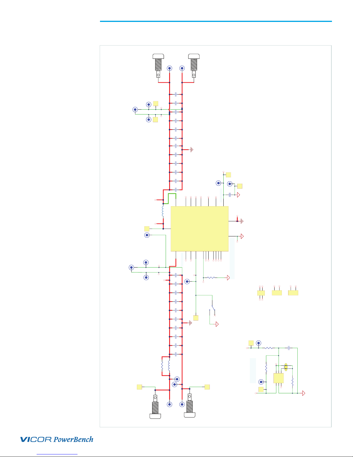
6. Loop compensation mode selection (S202): Used to select one of the following:
Local Sense (LS): default. Single ended feedback loop using the internal to the regulator
operational transconductance amplifier. +VOUT Lug is the local sensed location. +VOUT lug is
connected to the Error Amplifier Inverting Input (EAIN) through a voltage divider network.
Remote Sense (RS): Non-isolated remote sensing option using the internal to the regulator
independent differential amplifier which outputs (VDIFF) is in turn connected to the
transconductance amplifier input (EAIN) pin. Remote sensing is achieved using +VRS and –VRS
test points. Resistors R223 and R224 are 100Ωcatch resistor placed to prevent an open loop
condition if accidentally switched to this mode.
7. Trim mode selection (S201 or S203): Switch (S201) and trim potentiometer (R206) are associated
with local sense loop while switch (S203) and trim potentiometer (R221) are associated with remote
sense selection. Both Switches (S201 and S203) provide the following trim modes:
Fixed Trim (FIXED): default. Fixed resistor divider is used to set regulator output to the nominal
datasheet output voltage.
Adjustable Trim (ADJ): selection allows the use of trim potentiometer (R206 or R221) to
exercise the full output voltage range. Turn counterclockwise to increase the output voltage
and clockwise to decrease the output voltage. The trim potentiometer at either lowest or
highest point can only exercise the voltage range defined in the datasheet as valid operational
range within tolerance limits. If preferred, through-hole receptacles are available to bypass the
potentiometer with external leaded resistor.
8. Header-jumper (J201): Default setting is all three jumper sockets populated. This header provides
the following function:
Pin 1 and pin 2 can be used to inject the isolated signal of a network analyzer through
(R211= 49.9Ω) used for bode plot measurement in order to evaluate the stability in
local sense mode.
Pin 3 and pin 4 are used to short the Lighting (LGH)/Constant Current (CC) Sense Input to
SGND. LGH header pin 4 is used for lighting and constant current type applications. When not
in use the constant current mode (CC mode), the LGH pin should be connected to SGND. Refer
to the product datasheet for availability of this pin function.
Pin 5 and pin 6 can be used to inject the isolated signal of a network analyzer through
(R214 = 49.9Ω) used for bode plot measurement in order to evaluate the stability in remote
sense mode.
9. Soft-start capacitor (C123): Capacitor connected to regulator TRK pin and SGND. The soft-start
time is set with an internal 47nF capacitor to roughly 0.94ms. C123 can be added to further stretch
the soft-start ramp CTRK = (tTRK_DESIRED x 50E-6) – 47E-9 where ITRK = 50µA.
10. Internal operational transconductance amplifier compensation network (C201, R212, C203, C202):
this network provides flexibility during loop compensation design to adjust the compensation.
For the purpose of this evaluation board C201 in series to the internal R(ZI) of 5kΩis used.
The maximum mid-band gain that can be achieved when using the internal R(ZI) is roughly
(20•log(R(ZI)•gm•VREF/VOUT_SET). With a reference voltage of 0.99V and output voltage of 5V max
midband gain is ~14dB. R212 + R(ZI) and C203 in series can be used to further increase the mid-
band gain. C202 can be used to lower the high frequency pole if desired. The high frequency pole
is set internally to ~1.7Mhz using a C(HF) = 56pF.
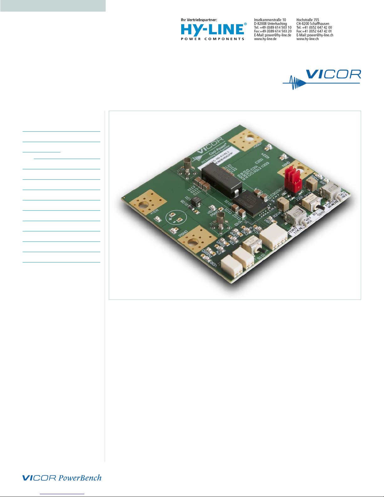
11. Output lugs: Sized for #10 hardware. Use these lugs to connect the output directly to the load.
12. Output oscilloscope probe Jack (J102): Used for making accurate scope measurements of the
output voltage (e.g. ripple). The jack is directly compatible with many common passive voltage
probes models. Remove the grounding lead and insulating barrel of the probe and insert the probe
tip and barrel directly into the jack, ensuring that the probe tip sits in the center socket of the jack.
To avoid the risk of an inadvertent short circuit, do not attempt to install while power is applied.
This Johnson Jack is kelvin connected to C113 positive pin.
13. Output filter: 12x 47µF output ceramic capacitors 1210 (C111- C122). Is used to achieve <1.5% of
VOUT peak to peak ripple.

UG:307 vicorpower.com Applications Engineering: 800 927.9474 Page 8
Test Points Description
Each square point test point can be used with standard probes, clips or hooks. All test points are
labeled on the board. Each test point is accompanied with an adjacent socket for adding a test lead or
to facilitate wiring to external circuitry.
Reference Designator/
Functional name Description
+VIN, PGND Input voltage test points provide connection to input lugs. Use Kelvin (J101) to
avoid interconnection losses if accuracy is desired.
+VOUT, PGND Output voltage test points provide connection to output lugs. Use Kelvin (J102)
to avoid interconnection losses if accuracy is desired.
VDR
A 5.1V auxiliary supply with max loading of 2mA. If used this pin must
have a series resistance such as R103 = 1kΩwith a decoupling cap of
0.1µF such as C124.
PWRGD Power good indicator. During a regulator fault this pin is pulled internally
to signal ground.
EN Input to the regulator. If left floating or driven high (VEN_MAX = 5.5V) regulator
will be enabled.
SGND Internal logic ground.
TRK Soft-start and track input. An external capacitor may be connected between TRK
pin and SGND to increase the rise time of the internal reference during soft-start.
COMP Compensation pin. An internal 5KOhm is in series between this pin and the EAO
pin. A default C201 = 4.7nF is used.
EAO Error Amp output. External connection for additional compensation and
current sharing.
EAIN_R Error Amp Inverting Input separated with R222 = 0Ω.
VSP Non-inverting input to an independent differential amplifier.
+VRS, -VRS Non-isolated remote sense input. When selecting remote sense feedback connect
to the regulation point at the load.
J201 Used to inject the isolated signal of a network analyzer into the feedback look.
Pin injection point is depend on loop selection.
Table 1
Test Point Descriptions

UG:307 vicorpower.com Applications Engineering: 800 927.9474 Page 9
Sockets Description
Each socket accepts 0.015 – 0.025 inch diameter leads for easy installation of solid wires and through-
hole components for use with external circuit and test equipment.
Reference
Designator
(Shown in
Assembly Drawing)
Functional Name Description
TP101, TP103 Input
voltage (+VIN, -VIN)
Input voltage test points. +VIN location is after input filter
inductor. –VIN is connected to PGND.
TP105, TP103 Input Capacitor (CIN)
Sockets are used for easy installation of through-hole
100V rated aluminum-electrolytic capacitor. Ensure proper
polarity with short leads while installing.
TP112 Power Ground (PGND)
This test point is in close proximity of the voltage switching
node (VS1) test point. To be used when probing VS1 to
minimizing ground loop.
TP104, TP102 Input
voltage (+VOUT, -VOUT) Output voltage test points. –VOUT is connected to PGND.
TP201, TP203 Local sense trim resistor
test points (R206)
Used for easy installation of a fixed through-hole resistor
across the Trim pot. Used only when Switch (S202) is in
local sense position and switch (S201) is in Adj position.
TP215, TP216 Remote sense trim
resistor test points (R221)
Used for easy installation of a fixed through-hole resistor
across the Trim pot. Used only when Switch (S202) is in
remote sense position and switch (S203) is in Adj position.
TP110 VDR
A 5.1V auxiliary supply with max loading of 2mA. If used
this pin must have a series resistance such as R103 = 1kΩ
with a decoupling cap of 0.1µF such as C124.
TP111 PWRGD Power good indicator. During a regulator fault this pin is
pulled internally to signal ground.
TP107 EN Input to the regulator. If left floating or driven high
(VEN_MAX = 5.5V) regulator will be enabled.
TP109 SGND Internal logic ground.
TP108 TRK
Soft-start and track input. An external capacitor may be
connected between TRK pin and SGND to increase the rise
time of the internal reference during soft-start.
TP207 COMP Compensation pin. An internal 5kΩis in series between this
pin and the EAO pin. A default C201 = 4.7nF is used.
TP209 EAO Error Amp output. External connection for additional
compensation and current sharing.
TP208 EAIN_R Error Amp Inverting Input separated with R222 = 10kΩ.
TP210 VSP Non-inverting input to an independent differential amplifier.
TP211, TP212 Remote Sense
input (+VRS, -VRS)
Non-isolated remote sense input. When selecting remote
sense feedback connect to the regulation point at the load.
Table 2
Sockets Descriptions

UG:307 vicorpower.com Applications Engineering: 800 927.9474 Page 10
Schematic
J101
J102
PROBE-070x135SMD
1
+VIN
TP_TH
TP_TH
TP_TH
TP_TH
TP_TH
PROBE-070x135 SMD
1
VS1
PROBE-070x135 SMD
1-VOUT
1+VOUTVS1
PROBE-070x135 SMD1
+VOUT
1
TP_VIN+TP_VIN-
TP_VOUT+TP_VOUT-
1206
R105
1 2
L101
VIN
+VIN_LUG+VOUT_LUG
0404
L102
1210
C101
1210
C102
1210
C103
1210
C104
1210
C105
1210
C106
1210
C107
1210
C108
1210
C109
1210
C110 C111 C112 C113 C114 C115 C116 C117 C118 C119 C120 C121 C122
TP_TH
TP_TH
-VOUT_LUG
-VIN_LUG
VDR =5.1V, 2mAmax
ElectrolyticCapacitor place holder
VSPVDR
TP_TH
1
VSNPWRGD1
VDIFF
EN
PROBE-070x135 SMD
1
EN
LGH
1E
EN
1F
SYNCI
4K
VDIFF 3A
EAIN 2A
VSP5A
VSN4A
COMP 1B
SYNCO
3K
TEST1
2K
TEST3
1J
TEST4
1H
TEST2
1K
TRK1C
SGND
EAO1A
VDR
5K
VOUT
PWRGD
1G
VS1
PGND
VIN
HiddenPinsinSymbol
PS101
HV ZVSBuck10x14mm SIP
EAIN
SYNCI
PROBE-070x135SMD
1
-VIN
SYNCO
EAOLGH
TEST1
40538
2
3
1
S101
SW_GT11MSABE COMPTEST2
0603
R101
TEST3
TP_THTEST4
C_TRK-INT=0.047uF
TRK
PROBE-070x135SMD
1
TRK
0603
C123
DNP
TP_TH
Do notconnect SGND to PGND in layout.
Connectionismadeinternall
y
to themodule
SGND PGND
PROBE-070x135 SMD
1
SGND
PROBE-070x135 SMD
1
VDR
VDR
Green:Power good
Red: Otherwise
PWRGD
3
1
4
2
J108
CN8_AVX_SERIES_9276
TP_TH
SGND EN
TP_TH
TRK
0603
R103
EAO
PROBE-070x135SMD
1
PWRGD
0603
R102
PCBNumber
SC70 6PIN IC
2
1
3
1A
GND
Y1
4
5
6
A2
VCC
Y2
U101
SGND
Y1
SYNCI
Y1
CN_2WAY-AVX
1
2
J109
0603
C124
DFN1010C 4PIN
42
31
D101
GREEN
RED
SGND
0603
R104
SYNCO
CN_2WAY-AVX
1
2
J110
Figure 3
PI352x Evaluation Board
Schematic Page 1

UG:307 vicorpower.com Applications Engineering: 800 927.9474 Page 11
Schematic (Cont.)
FIDUCIAL
FID1
FIDUCIAL
FID2
FIDUCIAL
FID3
FIDUCIAL
FID4
POGOpins
TP_EN
13
TP_-VIN
1
TP_TM
15
T
P
_
E
N
T
P
_
-
V
I
N
T
P
_
T
M
TP_ISP26
TP_VDIFF22
TP_SYNCI
5TP_VDR
4
TP_SYNCO
6
TP_COMP19
TP_VSP24
TP_TEST1
8TP_NC
7
TP_TEST2
9
TP_EAO 20
TP_IMON25
TP_+VIN
2
TP_TEST3
10
TP_VBIN
3
TP_SGND17
TP_EAIN_R21
TP_PWRGD
12 TP_TEST4
11
TP_EN_BUS
14
TP_TRK18
TP_VSN 23
TP_TEST5
16
TP_VS+29
TP_-VOUT 30
TP_+VOUT 31
TP_ISN27
TP_RAL 28
BRND_TP
SGNDTP_VIN-
0603
R201
TEST1
TP_VIN+TRK
COMP SGND
0603
R202
TEST2
EAOVDR
SYNCIEAIN_R
0603
R203
TEST3
VDIFFSYNCO
VSN
0603
R204
TEST4
VSPTEST1
TEST2
TEST3
TEST4
PWRGD
EN
TP_VOUT+
TP_TH
TP_TH
LGH
TP_VOUT+
RPOT
R206
0603
R207
0603
R208
0603
R209
0603
R210
0603
R211
S1 S2
TP_TH
SW_DPDT-G3T22
3
21
6
54
S201
PROBE-070x135 SMD
1
EAIN_R
EAIN_R
TP_TH
**Graphical representation of "Internal"
CONN-6PIN
3
2
1
4
5
6
J201
S1
Transconductance_OPAMP_Circuit Install shunt blocks across pins 1 & 2
S2PROBE-070x135 SMD1
COMP
and across pins 5 & 6 for regular operation
LGH
COMP
S5
0603
R212
R(ZI)
S6
R(ZI) = 5K Ohm
0603
R222
TP_TH
0603
C201
40538
2
3
1
S202
SW_GT11MSABE
_
DNP
EAIN
EAO
PROBE-070x135 SMD
1
EAO
0603
C203
REF_0.9V
+
C_EAIN-INT
DNP
C(HF)
C_EAIN-INT = 56pF
0603
C202
DNPC(HF) = 56pF
TP_TH
PROBE-070x135 SMD
1
VSP
+VOUT
0603
R223TP_TH
PROBE-070x135 SMD
1+VRS
VSP
0603
R213
0603
R214
0603
R215 S5 S6
+
VDIFF
SW_DPDT-G3T22
32
1
65
4
S203
_
VSN
DIFF_OPAMP
*Graphical representation of "Internal"
TP_TH
PROBE-070x135 SMD
1-VRS
Transconductance_OPAMP_Circuit
0603
R216
0603
R217
0603
R218
0603
R219
0603
R220
RPOT
R221 0603
R224
TP_THTP_TH
MODULATOR
Figure 4
PI352x Evaluation Board
Schematic Page 2

UG:307 vicorpower.com Applications Engineering: 800 927.9474 Page 12
TOP VIEW
R105
L102
R224
J108
D101
R206
R212
C203
C202
C123
C122
C121
C120
C113
C112
C111
C104C103
C102 C101
PS101
PGND
PGND
+VOUT
+VIN
TP208
TP209
TP210 L101
C201
R221
TP106
TP105
+VRS
-VOUT
-VRS
TP207
TP109
TP108
+VIN
+VOUT
-VIN
J101
J102
TP103
TP101
TP104
TP102
COMP
EAIN_R
EAO
J201
PWRGD
SGND
TP107
TP110
TP111
TP201
TP203
TP211
TP212
TP215
TP216
TRK
VDR
VSP
S203
EN
J109
J110
S101 S202
S201
TP112
VS1
C302
C303
R307
R308
R309
Cool-Power R
ZVS Switching Buck Regulator
PCB# 44841
Reserved
Serial # Label
Figure 5
PI352x Evaluation Board
Assembly, Top Side

UG:307 vicorpower.com Applications Engineering: 800 927.9474 Page 13
BOTTOM VIEW
R223
R222
R214
C124
U101
R209
R208
R207
R104
R211
R101
R103
R102
C119
C118
C117
C116
C115
C114
C110
C109
C108
C107
C106
C105
R210
R213
R215
R216
R217
R218
R219
R220
J104
J106
J105
J107
R201
R202
R203
R204
C301
LGH_IN
R301
R302R303
R304
R305
R306
Figure 6
PI352x Evaluation Board
Assembly, Bottom Side

UG:307 vicorpower.com Applications Engineering: 800 927.9474 Page 14
Bill of Materials
Reference
Designator Description QTY Manufacturer Manufacturer
Part Number
C101-C110 CAP X7R 2.2µF 10% 100V 1210 10 Murata GRM32ER72A225KA35L
C111-C122 CAP X7R 47µF 10% 10V 1210 12 Murata GRM32ER71A476KE15L
C124 CAP X7R .1µF 10% 100V 0603 1 Murata GRM188R72A104KA35J
C201 CAP X7R 4700pF 5% 100V 0603 1 TDK C1608C0G2A472J080AC
CKIT BOM CONN KIT ARRAY DEMO BD 1 Arnold Industries 26647
COMP, EAIN_R,
EAO, EN,
PWRGD, +VRS,
-VRS, SGND,
TRK, VDR,
+VIN, PGND,
+VOUT, PGND,
VS1, VSP
TEST POINT, SURFACE MOUNT 16 Keystone
Electronics 5017
J101, J102 JACK VERTICAL MECH THRU HOLE 2 Tektronix 131-5031-00
J108 CONN 4 POS WIRE TO BOARD SMD 1 AVX 009276004021106
J109, J110 CONN 2 POS WIRE TO BOARD SMD 2 AVX 009276002021106
J201 HEADER 6 PIN STRAIGHT SMT 1 FCI 95278-101A06LF
JMPR_1,
JMPR_2,
JMPR_3
JUMPER SOCKET 2POS 2.54mm
WHANDLE 3 TE Connectivity 2-881545-2
L102 INDUCTOR WW 65nH 15% 19A 0404 1 Eaton FP0404R1-R065-R
PAD_1, PAD_2,
PAD_3, PAD_4
ADHESIVE-BACK BUMPER,
7/16"x13/64" 4 3M SJ5003
R101, R201,
R202, R203,
R204, R222,
R306
RES 0ΩJUMPER 1A 0603 7 KOA Speer RK73Z1JTTD
R102 RES 10kΩ1/10W 1% 0603 1 KOA Speer RK73H1JTTD1002F
R103 RES 1kΩ1/10W 1% 0603 1 KOA Speer RK73H1JTTD1001F
R104 RES 2.4kΩ1/10W 1% 0603 1 KOA Speer RK73H1JTTD2401F
R105 RES 0.51Ω1/4W 5% 1206 1 KOA Speer SR732BTTDR51J
R206, R221 RES TRIM POT 5kΩ1/4W 10% SMD 2 Bourns 3224W-1-502E
R207 RES 7.50Ω1/10W 1% 0603 1 KOA Speer RK73H1JTTD7R50F
R208 RES 1.18kΩ1/10W 0.1% 0603 1 Panasonic ERA3AEB1181V
R209 RES 449Ω1/10W 0.1% 0603 1 KOA Speer RN731JTTD4990B25
R210 RES 4.81kΩ1/10W 0.1% 0603 1 Vishay TNPW06034K81BEEA
R211, R214 RES 49.9Ω1/16W 0.1% 0603 2 Susumu RG1608P-49R9-B-T5
R213, R219 RES 10.2kΩ1/10W 0.1% 0603 2 Vishay TNPW060310K2BEEA
R215, R218 RES 2.74kΩ1/16W 0.1% 0603 2 Susumu RG1608P-2741-B-T5
Table 3
PI352x Common Components

Rev 1.0 03/17 vicorpower.com Applications Engineering: 800 927.9474 Page 15
Bill of Materials (Cont.)
Reference
Designator Description QTY Manufacturer Manufacturer
Part Number
R216 RES 1.27kΩ1/10W 0.1% 0603 1 Vishay TNPW06031K27BEEA
R217 RES 453Ω1/10W 0.1% 0603 1 Susumu RG1608P-4530-B-T5
R220 RES 4.64kΩ1/16W 0.1% 0603 1 Susumu RG1608P-4641-B-T5
R223, R224 RES 100Ω1/10W 1% 0603 2 KOA Speer RK73H1JTTD1000F
S101, S202 SW Horizontal SPDT 1 POS SMD 2 C&K GT11MSABETR
S201, S203 SW TOGGLE DPDT G3T22AH SMD 2 NKK G3T22AH
TP101, TP102,
TP103, TP104,
TP105, TP106,
TP107, TP108,
TP109, TP110,
TP111, TP112,
TP201, TP203,
TP207, TP208,
TP209, TP210,
TP211, TP212,
TP215, TP216
PIN RECPT .015/.025 DIA 0667 SER TH 22 Mill-Max 0667-0-57-15-30-27-1
U101 IC SCHMITT TRIGGER INVERTER DUAL
SC70-6 1 Fairchild NC7WZ14EP6X
C123, C202,
C203, C301,
C302, C303,
D101, J104,
J105, J106,
J107, LGH_IN,
R212, R305,
R307, R308,
R309
NOT APPLIED 13
Reference
Designator Description QTY Manufacturer Manufacturer
Part Number
Evaluation board number: PI3525-00-EVAL1
PCB SNGLTD PCB PI3225-00-EVAL1 1 VICOR POWER
COMPONENT 44841
PS101 COOL-POWER NI BUCK REG
60V/5V 20A 1VICOR POWER
COMPONENT PI3525-00-LGIZ
L101 IND 230nH 10% 70A 22.2X8.2 1 EATON FP2207R1-R230-R
Table 3 (Cont.)
PI352x Common Components
Table 4
PI352x Design Specific
Components
This manual suits for next models
1
Table of contents
Other VICOR Motherboard manuals

VICOR
VICOR VI Chip VTM User manual

VICOR
VICOR PI3741-0x-EVAL1 User manual

VICOR
VICOR ChiP DCM3623 User manual

VICOR
VICOR VI Chip High-Voltage BCM User manual

VICOR
VICOR VITA62 3U User manual

VICOR
VICOR DCM2322 User manual

VICOR
VICOR VI Chip BCM User manual

VICOR
VICOR VI Chip VTM User manual

VICOR
VICOR PI3740-00-EVAL1 User manual

VICOR
VICOR HD Series User manual