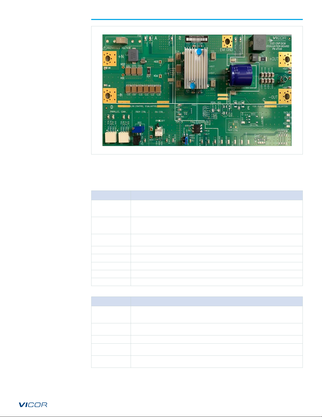
VICOR DCM2322 User manual

UG:020 Page 1
Introduction
The Analog Control DCM2322 ChiP evaluation board described in this document is designed to be used
with the DCM family of isolated, DC-DC converters. The DCM2322 board is used for the analog control,
low input voltage DCM2322 ChiP products.
The DCM evaluation board can be configured for various enabling and fault-monitoring schemes,
as well as to exercise various modes of trimming, depending on the application requirements. The
evaluation board can be used to evaluate DCMs in either a standalone configuration or as an
array of modules.
Operation Mode Options
Operation mode of the DCM can be selected based on the voltage seen by the DCM at its EN pin at first
start up following application of VIN. Two operation modes that can be selected are:
1. Array mode (default): the EN pin is permitted to float at initial start up.
The DCM enables the output and latches in array mode of operation.
2. Enhanced VOUT Regulation mode: applying a specified voltage level on the EN pin during initial
start up will latch the DCM in enhanced VOUT regulation mode.
Enable options:
1. On-board mechanical switch (default)
2. External control
Trim options:
1. Fixed trim operation (default): the TR pin is permitted to float at initial start up.
The DCM disables output trimming and the output trim is programmed to the nominal rated VOUT.
2. Variable trim operation, on-board variable resistor: The trim pin voltage is ratiometric,
with a rheostat working against a pull-up resistor inside the DCM to VCC.
3. Variable trim operation, off-board control: The trim pin voltage is controlled via external
programming control, which is referenced to the –IN of each specific DCM in the system.
Fault monitor options:
1. On-board LED: the FT pin drives a visible LED for visual feedback on fault status.
2. On-board optocoupler: the FT pin drives an on-board optocoupler to bring
fault status across the primary-secondary isolation boundary.
Contents Page
Introduction 1
Contents 3
Features 3
Board Description 4
General Components 4
Test Points Description 5
Schematic 6
Assembly Drawing 7
Bill of Materials 8
Recommended
Test Equipment 10
Basic Connections 10
Board Operation Details 10
EN (Enable) 11
Trim Control 12
Chassis Ground / EMI_GND 13
Paralleling 13
VamshiKrishna Domudala
Applications Engineering
Analog Control DCM2322 ChiP™
Evaluation Board
USER GUIDE | UG:020
INFORMATION SUBJECT TO CHANGE WITHOUT NOTICE

UG:020 Page 2
IMPORTANT NOTICE:
Hazardous voltages are present on the DCM Evaluation Board under power.
PERSONAL CONTACT WITH LINE VOLTAGE MAY RESULT IN SEVERE INJURY, DISABILITY, OR
DEATH. IMPROPER OR UNSAFE HANDLING OF THIS BOARD MAY RESULT IN SERIOUS INJURY
OR DEATH.
Read the precautions below entirely BEFORE using the DCM Evaluation Board. Do not operate the
evaluation board unless you have the appropriate safety precautions in place on your bench to
guarantee safety.
The list below is not comprehensive and is not a substitute for common sense and
good practice.
During operation, the power devices and surrounding structures can be operated
safely at high temperatures.
Remove power and use caution when connecting and disconnecting test probes
and interface lines to avoid inadvertent short circuits and contact with hot surfaces.
Never use a jumper in place of the fuse.
When testing electronic products always use approved safety glasses. Follow good
laboratory practice and procedures.
Avoid creating ground loops when making measurements of the isolated input
or output voltage.
Care should be taken to protect the user from accidental contact when
under power.
Care should be taken to avoid reversing polarities if connecting to the opposite
(solder) side of the board.
The product evaluation boards described in this document are designed for
general laboratory evaluation, and are not suitable for installation in
end user equipment.
Refer to the specific DCM module data sheet for electrical, thermal, and mechanical
product details.

UG:020 Page 3
This board provides a convenient way to evaluate/demonstrate the performance of Vicor DCM products.
Kelvin connections are provided for accurate voltage measurements on power nodes. Sockets are
provided to permit quick installation and changing of bulk filtering capacitors. The evaluation board also
provides lugs for input/output connections, test points and sockets for easy connection to standard test
equipment, and a high-performance air-cooled heat sink assembly.
Contents
The evaluation board arrives with the following contents:
1 x DCM evaluation board
1 x top heat sink assembly (pre-installed)
1 x hardware kit
Features
The DCM evaluation board has the following features:
1. Input and output lugs for source and load connections
2. Input fuse (appropriately rated)
3. Basic input filtering, including sockets to add through-hole input aluminum-electrolytic capacitors
for additional source decoupling
Note: The filtering used in the evaluation board is for demonstration purposes only and might not be
the optimal solution for all applications. For optimal filter design for parallel array application, consult the
DCMDesignGuide, data sheet of the DCM in use and the online filter design tool at:
http://app2.vicorpower.com/filterDesign/intiFilter.do
4. Basic output filtering, including sockets to add through-hole output
aluminum-electrolytic capacitors
5. Toggle switch for enabling and disabling the DCM via the ENABLE pin
6. Trim control selection
a. Using potentiometer
b. Using external voltage source
c. Open, to disable trimming and latch the model nominal trim condition
7. Provisions to replace input and output differential mode inductors with wire loops,
for oscilloscope/shunt based current measurements
8. Oscilloscope probe jack for accurate, high-frequency output voltage measurements
9. Dual paralleling connectors for ENABLE, TRIM, FAULT and PRI_SG signal connections, for daisy
chaining control to other DCM evaluation boards in an array
10. Kelvin voltage test points for all power pins
11. Top heat sink assembly for the DCM

UG:020 Page 4
Board Description
The following section provides a detailed description of the evaluation board components, test
points and sockets.
General Components
1. DCM (PS01).
2. Input lugs: Sized for #10 hardware. Use these for making connection to the input source.
This board does not contain reverse polarity protection. Check for proper polarity before
applying the power.
3. Input fuse (F01 & F02): Appropriately rated for the DCM model on the board.
4. Input filter: Ceramic input capacitors (C01 – C03, C05 – C10), filtering inductor (L01, L02) and
damping resistor (R04) provide input filtering. Sockets (H01 – H02) can be used for easy
installation of aluminum-electrolytic input capacitors. This board also adds H05 – H06 for
additional input bypassing.
5. Enable / Disable switch (SW01): When actuator is in top position towards “ON” text on the
board, the ENABLE pin will be open and the DCM will be enabled. When actuator is in bottom
position towards “OFF” text on the board, the ENABLE pin will be connected to PRI_SG and
the DCM will be disabled. When switch SW01 is ON, an external voltage source can control the
ENABLE state.
6. Header-jumper for trim control (J03): Provides the option to enable the trim function to set the
DCM programmed trim value via either the on board trim rheostat or an external voltage source:
a. Using potentiometer (R02)
b. Using external voltage source.
7. Output lugs: Sized for #10 hardware. Use these lugs to connect the output directly to the load.
8. Output oscilloscope probe Jack (J13): Used for making accurate scope measurements of the
output voltage (e.g. ripple). The jack is directly compatible with many common passive voltage
probes models. Remove the grounding lead and insulating barrel of the probe and insert the
probe tip and barrel directly into the jack, ensuring that the probe tip seats in the center socket
of the jack. To avoid the risk of an inadvertent short circuit, do not attempt to install while power
is applied.
9. Output filter: Filtering inductor (L04) and damping network (L03, R24), and ceramic output
capacitors (C21 – C22, C24 – 26, C28, C31 – C32) provide output filtering. Sockets H08 – H09 can
be used for easy installation of aluminum-electrolytic output capacitors.
10. Dual paralleling wire-to-board connectors (J07 and J08): Used for bussing control signals
and their reference (ENABLE, TRIM, FAULT and PRI_SG) across board assemblies during parallel
operation. The connector style provides simple “strip and insert” use with 18 – 24AWG solid wires.
Once inserted, a spring loaded barb retains each wire with no need for soldering. To release the
wire, insert a thin bladed tool (AVX 06-9276-7001-01-000 or similar) into the slot above each
wire entry point.

UG:020 Page 5
Figure 1
DCM2322 evaluation
board photo, top side
Test Points Description
Test nodes are labeled and include a SMT test point for attaching miniature probes, clips or hooks.
Table 1
Primary referred
test point descriptions
Table 2
Secondary referred
test point descriptions
Name Description
+IN_FUSED,
+IN_FILT,
–IN
Provide measurement test points for the input voltage to the board in various locations, rela-
tive to the –IN board lug. +IN_FUSED is taken after input fusing, +IN_FILT is taken after the
input filtering network.
+IN_DCM,
–IN_DCM
Provide Kelvin connection to input pins of the DCM. Use these test points for measuring the
input voltage at the module, excluding errors due to finite connection resistance leading up to
the module.
PRI_SG Test point for Signal Ground on the primary/input side of the isolation boundary. This is the
reference for all primary side control circuitry and all control pins of the DCM.
EXT_EN Test point to drive the ENABLE signal (relative to PRI_SG) using an external source.
PRI_EN Test point to measure the ENABLE signal (relative to PRI_SG).
EXT_TRIM Test point to drive the TRIM signal (relative to PRI_SG) using an external source.
PRI_TR Test point to measure the TRIM signal (relative to PRI_SG).
PRI_FT Test point to measure the FAULT signal (relative to PRI_SG).
Name Description
+OUT_DCM,
–OUT_DCM
Output voltage test points provide Kelvin connection to output pin group of the DCM. Use
these test points for measuring the output voltage at the module, excluding voltage errors
due to finite connection resistance and the module output current.
+OUT,
–OUT
Provides measurement test points for the output voltage in various locations, relative to the
–OUT board lug.+OUT is taken at the +OUT board lug.
SEC_SG Test points for the +5V bias supply return, and for measuring the FT_SEC fault monitor output.
FT_SEC Test point to measure the FAULT signal relative to SEC_SG once it has passed through the
opto-coupler, if used. Bias power must be supplied to +5V for voltage output to appear here.
+5V Test point to provide a bias voltage (relative to secondary ground) for the fault opto-coupler,
if used.

UG:020 Page 6
Schematic
J02
-IN
TP27
TP28
J12
+OUT
J11
-OUT
-OUT
TP47
+OUT
-OUT
L04
+OUT
TP48
R24
CHASSIS-GND
-IN_DCM
+IN_DCM
+OUT_DCM
3
1
4
2
J07
PRI_EN
PRI_FT
R06
D01
PRI_SG
ENABLE CONTROL
R14PRI_SG
TP14
TP15
TP16
C04
PRI_SG
PRI_SG
EXT_EN
TP02
C17
TP12
3
1
4
2
J08
1
2 5
43
6
M01
R13
PRI_SG
R09
R17
SEC_SG
FT_SEC
TP17
R03
CHASSIS_GND
J09
R07
+IN_DCM
TP10
-IN_DCM
TP11
+OUT_DCM
TP29
-OUT_DCM
TP30
PARALLELINGCONNECTORS
+IN_FUSED
TP04
-IN
TP03
-IN
+IN_FILT
TP13
+IN_DCM
-IN_DCM
+IN_FILT
TP05
PRI_FT TP08
PRI_TR TP06
PRI_EN TP07
PRI_TR
PRI_EN
PRI_FT
PRI_SG
PRI_SG TP09
R16
+5V
FAULTINDICATOR
2
3
1
SW01
ON/External_Ctrl
OFF
3
1
4
2
J05
H08
H09
H02
H01
SEC_SG
TP41 TP43
+5V
+OUT 7
+
O
U
T
T
7
-IN
5
+IN
1
-OUT6
CL
4
DA
3
AD
2
PRIMARYSECONDARY
ISOLATIONBOUNDRY
DCM2322
PS01
GND
HS01
J13
-IN_DCM
-OUT_DCM
+IN_DCM
+OUT_DCM -OUT_DCM
PRI_TR
TRIM CONTROL
R02
PRI_SG
EXT_TRIM
TP01
Trim_Pot
External_Trim
R01
C16C18
C15C19
C30C34
C33
C29
R32R35
1
132
S03
C21C22C24C25C26C28C31C32
-OUT
+OUT
R04
C05C06C07C08C09C10
S02
S01
C01C02C03
38546-R22
SRP4020
L02
H04
H03
C13
PRI_EN
PRI_FT
PRI_TR
R08
C12
PRI_SG
R10
R12
R11
R36
AD_RXD
SGND
GENERIC_PART
P/N
F02
J01
+IN
+IN
1
132
S04
46244-72N
INDUCTOR
0.072
L03
47451-226
2420
22
63
C10A
47451-226
2420
22
63
C09A
47451-226
2420
22
63
C08A
47451-226
2420
22
63
C07A
47451-226
2420
22
63
C06A
47451-226
2420
22
63
C05A
3
1
4
2
J03
i
PRI_DC
i
PRI_DC
i
PRI_DC
i
PRI_GND
i
PRI_GND
i
PRI_GND
iPRI_GND
i
PRI_GND
i
PRI_GND
i
PRI_GND
i
PRI_GND
i
PRI_GND
i
PRI_GND
i
PRI_GND
i
PRI_GND
i
PRI_GND
i
PRI_GND
i
PRI_GND
i
SEC_DC
i
SEC_DC
i
SEC_DC
i
SEC_GND
iSEC_GND
i
GNDi
GND
iSEC_GND
+OUT_DCM
i
SEC_GND
i
PRI_GND
iSEC_GND
iSEC_GND
iSEC_GND
i
PRI_GND
i
PRI_GND
iPRI_GND
i
PRI_GND
i
PRI_DC
i
PRI_DC
i
PRI_DC
i
PRI_GND
+IN_FUSED
TP51
-OUT_DCM
H05
H06
47392-2R2
4040
2.2
L01
GENERIC_PART
30276
Value
F01
iSEC_DC
Figure 2
DCM2322 evaluation board
schematic

UG:020 Page 7
TOP VIEW
FC1 FC2
Assembly Drawing
Figure 3
DCM2322 evaluation board,
assembly drawing, top side

UG:020 Page 8
Table 3
DCM evaluation board BOM Reference
Designator Description Manufacturer Manufacturer
Part Number
Common Components
C01, C02, C03,
C05, C06, C07,
C08, C09, C10,
C13
CAP X7T 2.2µF 20% 250V 2220 TDK C5750X7T2E225M250KA
C04 CAP X7R 0.10µF 10% 16V 0603 AVX 0603YC104KAT2A
C12 CAP X7R 0.001µF 10% 50V 0603 TDK C1608X7R1H102K080AE
C15, C16,
C18, C19
CAPY2 X7R 4700pF 10% 250V 2220
0.079MAXHT
Murata
Manufacturing GA355DR7GF472KW01L
C21, C22, C24,
C25, C26, C28,
C31, C32
CAP X7S 10µF 10% 100V 1210 Murata
Manufacturing GRM32EC72A106KE05L
C29, C33 RES 0Ω JUMPER 2A 1206 Vishay CRCW12060000Z0EC
C30, C34
CAP X7R 4700pF 10% 1kV 1206
Note: Capacitors are not rated for 3kV.
See product data sheet for
recommended capacitor.
KEMET Corporation C1206C472KDRACTU
D01 DLED RED 0805 Rohm SML-211UTT86
H01, H02, H03,
H04, H05, H06,
H08, H09
PIN RECPT .032/.046 DIA 0327 SER TH Mill-Max 0327-0-57-15-34-27-1
J03, J05 HEADER 4 PIN STRAIGHT SMT FCI 95278-101A04LF
J07, J08 CONN 4 POS WIRE TO BOARD SMD AVX 009276004021106
L01 IND 22µH 20% 5A 4040 Bourns SRP1038A-220M
L02 IND 220nH 20% 10A SMD Bourns SRP4020-R22M
L03 IND 72nH 20% 45A 2727 Vishay IFLR2727EZER72NM01
L04 IND 0.33µH 20% 50A SMD Wurth Elektronik Group 744309033
M01 IC 6 PIN OPTO SMD Vishay CNY17-3X017T
R01, R03, R10,
R11, R12, R14,
R16, R36
RES 0Ω JUMPER 1A 0603 KOA Speer Electronics RK73Z1JTTD
R02 RES TRIM POT 500kΩ 1/2W 10% TH NIDEC Copal Electronics CT-94EW504
R04 RES 1.5Ω 1W 5% 2512 KOA Speer Electronics RK73B3ATTE1R5J
R06, R13 RES 1kΩ 1/10W 5% 0603 KOA Speer Electronics RK73B1JTTD102J
R07, R09 RES 49.9kΩ 1/10W 1% 0603 KOA Speer Electronics RK73H1JTTD4992F
R08 RES 1kΩ 1/10W 1% 0603 KOA Speer Electronics RK73H1JTTD1001F
R17 RES 4.99kΩ 1/16W 0.1% 0603 Susumu RG1608P-4991-B-T5
R24 RES 0.050Ω 1W 1% 2512 Yageo RL2512FK-070R05L
R32, R35 RES 1Ω 1/16W 1% 0402 KOA Speer Electronics RK73H1ETTP1R00F
S01, S02,
S03, S04 1612 COPPER SHUNT EXCEL TOOL & DIE
CO, INC. 29581
SW01 SW Horizontal SPDT 1 POS SMD C&K Components GT11MSABETR
TP01, TP02, TP03,
TP04, TP05, TP06,
TP07, TP08, TP09,
TP10, TP11, TP17,
TP29, TP30, TP41,
TP43, TP47, TP48,
TP51
TEST POINT, SURFACE MOUNT Keystone Electronics 5017
HTSNK BOM ASSY 2223 XF PUSH PIN HTSINK
NO TIM MALICO INC 40478
J13 JACK VERTICAL MECH THRU HOLE Tektronix 131-5031-00
Bill of Materials

UG:020 Page 9
Table 4
Example: BOM additions,
components which are
model-specific
Reference
Designator Description Manufacturer Manufacturer
Part Number
Evaluation board number: DCM2322EA5N13A2T60
C17 CAP ALEL 680µF 20% 63V RADIAL 18x20 United Chemi Con ELXZ630ELL681MM20S
F01 FUSE 5A 125V PCD-5-R Eaton BK/PCD-5-R
PS01 DCM 2322 VICOR DCM2322TA5N13A2T60
Bill of Materials (Cont.)
General BOM rules for various DCM Evaluation Boards
PS01: This is the Vicor DCM, whose part number is coded in the evaluation board part number.
For example, evaluation board DCM2322EA5N13A2T60 uses DCM2322TA5N13A2T60.
F01: This is the input fuse. See the data sheet for the specific DCM for appropriate fuse needed to
meet listed safety agency approvals.
C17: This is the external output capacitor for the DCM. It is an Aluminum electrolytic with value that
satisfies the DCM data sheet COUT-EXT minimum.

UG:020 Page 10
Recommended Test Equipment
The following is a list of recommended test equipment.
1. Safety glasses
2. DC power supply: Refer to the specific DCM model data sheet to ensure the supply has
sufficient power and current capability, especially at low line, to satisfy current inrush when the
DCM is started
3. Electronic load: Refer to the specific DCM model data sheet to ensure the load has sufficient power
handling and current capability for testing
4. Cooling fan
5. Digital multi-meters (DMMs)
6. Oscilloscope and probes
7. Function generator
8. Auxiliary bench voltage supply (optional, for bias of secondary side fault monitor opto-coupler)
9. Interconnect wires, cables and fastening hardware
10. Calibrated input and output shunts, appropriately rated
11. Thin bladed tool for extracting wires from paralleling connectors
(AVX 06-9276-7001-01-000 or similar)
Basic Connections
Confirm bench equipment is powered off.
Connect the input DC power supply positive lead to the +IN input lug of the evaluation board,
connect the input power supply negative lead to the –IN input lug of the evaluation board.
Connect the EMI-GND lug of the evaluation board to a safety “green wire” earth ground.
Connect the +OUT lug of the evaluation board to the electronic load positive input, connect the
–OUT lug of the evaluation board to the electronic load negative input.
Direct airflow from the cooling fan through the DCM heat sink fins.
Have the latest DCM data sheet on hand for reference.
Board Operation Details
SW01 provides control over enable.
In the “OFF” position, the switch will connect PRI_SG the EN net, which disables the DCM.
In the “ON” position, PRI_SG is disconnected from the EN net.
External connection to EN is permitted using the PRI_EN test point. SW01 should be set to “ON” to
permit external control.
The J07 & J08 paralleling connectors can be used to connect EN nets across different boards.
Note: to enable the DCMs in a parallel array, all boards need SW01 set to “ON” to avoid pulling the
EN node low.

UG:020 Page 11
EN (Enable)
The EN pin provides two functionalities:
Enables and disables the DCM converter.
Selects Array mode or Enhanced VOUT Regulation mode.
The EN pin is referenced to the –IN pin of the converter. It has an internal pull up to VCC through
a 10kΩ resistor.
EN is an input only, it does not pull low in the event of a fault.
Enable/Disable Control
Output disable: when EN is pulled down externally below the disable threshold (VENABLE-DIS-TH),
the DCM converter will be disabled.
Output enable: when EN is allowed to pull up above the enable threshold (VENABLE-EN-TH) through the
internal pull up to VCC, the DCM converter will be enabled.
Selecting Array Mode or Enhanced VOUT Regulation Mode
The EN pin can also be used to select Array mode operation or Enhanced VOUT Regulation mode
operation. The DCM mode of operation is dependent on the voltage seen by the DCM at its EN pin at
first start up following application of VIN. The DCM will latch in selected mode of operation at the end
of soft start, and persist in that same mode until loss of input voltage.
At the first start up after application of VIN, if EN is allowed to float to:
A value above VENABLE-EN-TH, but below VREG-EN-TH, the DCM will implement
Enhanced VOUT Regulation mode.
A value above VARRAY-EN-TH and up to VCC, the DCM will implement
Array mode operation.
Note that the selected mode of operation is not changed when a DCM recovers from any fault
condition, or after a disable event through EN. The operation mode is reset only with cycling
of input power.
Figure 4
EN pin voltage thresholds
A
Disable
rray Mode
Enhanced V
OUT
Regulation Mode
V
ENABLE-EN-TH
V
ENABLE-DIS-TH
V
CC
V
REG-EN-TH
V
ARRAY-EN-TH
Note: Refer to the product data sheet for EN pin threshold voltages.

UG:020 Page 12
Trim Control
Jumper block J03 configures trimming.
With no jumpers installed, neither the trim potentiometer nor the test point for external trim
control is connected to the TR net. Note that the paralleling connectors always connect to
the TR net.
With a jumper loaded across J03.1 and J03.2, the trim potentiometer R02 is
connected as a rheostat between the TR node and PRI_SG.
With a jumper loaded across J03.3 and J03.4, the external trim test point is
connected to the TR node.
The DCM contains an internal pull-up resistor to VCC (3.3V nominal). When VIN is applied to the DCM
it samples the TR node voltage. If it has pulled up to VCC, the DCM disables trimming as long as it has
input power, and the programmed trim condition will be nominal rated VOUT of the DCM model.
If the TR node is not permitted to pull up to VCC when VIN is applied, trimming is enabled for as long
as the DCM has input power.
Note: Any load on the TR node may cause the DCM to select trim mode when VIN is applied,
including: the external trim test point (if selected with the jumper block), the trim potentiometer
(if selected with the jumper block), and other DCM evaluation boards attached to the
paralleling connectors.
The trim potentiometer adds a variable resistance between the TR node and PRI_SG, from between
0Ω nominal, to the value of the potentiometer (500kΩ). This resistance range will generate TR pin
voltages which cover the entire functional range of the TR pin. Care should be taken to ensure the
programmed trim condition is within the rated trim range of the DCM in order for the DCM to meet
specifications.
In a parallel set up using the J07 & J08 paralleling connectors, all boards besides the top one should
have the trim jumper select block at J03 open.
In a parallel set up with multiple DCM evaluation boards, each DCM contributes another internal
pull-up resistor to a 3.3V nominal rail. With any resistive based trimming of the TR node, the resultant
trim condition will be modified by the number of DCMs which are attached and have VIN applied.
Conversely with a voltage source applied to the TR node, adding additional DCMs to the system has
minimal impact on the resultant trim condition.
Fault Monitoring
Jumper block 05 configures how the FT node is monitored.
With no jumpers installed, neither the visible LED nor the opto-coupler is connected to the FT net.
Note that the paralleling connectors always connect to the FT net.
With a jumper loaded across J05.3 and J05.4, the visible LED at D01 and its bias resistor network
R09 & R32 are connected to the FT node.
With a jumper loaded across J05.1 and J05.2, the opto-coupler at M01 and its bias resistor
network R16 & R17 is connected to the FT node.
The DCM FT output is intended to be directly paralleled with the FT output of other DCMs in an array.
The FT node in an array forms a “wired-OR”, where any DCM can drive the FT node high.
Both the visible LED and the opto-coupler draw current from the FT node in a fault condition. The FT
pin on the DCM has limited drive-high capabilities, and so care must be taken to avoid excess loading
of the pin. To avoid overload, do not configure J05 to use both the LED and opto-coupler indicators
simultaneously. When connecting external circuitry or test equipment to the FT test point, ensure that
the maximum load on the FT node is within the DCM data sheet ratings.
In a parallel set up using the J07 & J08 paralleling connectors, all boards besides the top one should
have the fault jumper select block at J05 open.
When using the opto-coupler, the status of the FT node can be easily transferred to the secondary side
of the DCM(s) isolation boundary. To resolve the fault state on the secondary side, the collector side
of the opto requires a bias voltage. A 5V bench supply should be connected between the “+5V” and
“SEC_SG” test points. With no fault present, “FT_SEC” will be at 0V, and when a fault occurs and the
opto-coupler is active, “FT_SEC” will pull up to 5V, relative to SEC_SG.

UG:020 Page 13
Chassis Ground / EMI_GND
The heat sink assembly of the DCM is connected to the EMI_GND node of the board, as well as
the y-caps from each power connection of the DCM. A connection from the EMI_GND lug to earth
ground is required.
Paralleling
The paralleling and sharing performance of multiple DCMs can be easily demonstrated by stacking
multiple evaluation boards and interconnecting the inputs and outputs with standoffs to create
a parallel array. When operated in Aray mode, the DCM uses a negative load-line to implement
wireless droop-sharing in an array. Each DCM in an array operates in the same way as it does as a
standalone Array-mode unit. With equal trim conditions, the load is effectively shared across multiple
DCMs. Mismatches in this case are modest, and are further canceled by an effective negative voltage
vs. temperature coefficient. See the DCM data sheet for more detail on load line and temperature
coefficients. DCMs in an array require no de-rating of maximum output power or current.
DCMs in an array with mismatched trim conditions will not share the load equally at light- to
moderate-load conditions. As the load increases, one or more DCMs (starting with those with the
highest programmed output trim voltage) will go into current limit and their contribution to the overall
output current will plateau. For DCMs, current limit is not a fault condition, rather it is a valid constant-
current mode of operation and a DCM in current limit will provide constant current to the load. As long
as the load does not exceed the maximum load rating of the array of DCMs, the output voltage will
continue to be regulated by any remaining DCMs still in constant voltage mode. Even with mismatched
trim conditions, the array can be safely loaded up to the full rated array capacity.
The following connections and settings should be used for an array of DCM evaluation boards:
All DCMs in a parallel array must be the same model and must be configured to operate in
Array mode.
The boards should be physically stacked using metal standoffs at the +IN & –IN lugs,
the +OUT & –OUT lugs, and the EMI_GND lug. This also connects these nodes electrically so that a
single source, single load and earth ground connection can be made to the system.
The +IN lugs are not required to be connected together for an array of DCMs. The wireless
sharing does not require the same differential input voltage be present on all DCMs in the array.
In some applications dissimilar input voltages may be needed, which is fully supported.
The –IN lugs must be connected together if the paralleling connector is used, or if the EN, TR,
or FT pins are interconnected in any fashion. However if all control signals of all DCMs are fully
isolated from one another, then both the +IN and –IN lugs can remain independent across the
evaluation boards, and the DCMs can be operated with fully independent input supplies.
Standoffs must be sufficient in length to avoid contact between boards, and to permit airflow to
all DCMs in the system.
If coordinated enable control, trimming or fault monitoring is desired, then the paralleling
connectors J07 & J08 can be used to easily interconnect the PRI_FT, PRI_EN, PRI_TR_ and PRI_FT
nodes across boards.
The paralleling connectors at J07 & J08 can be used for coordinated enable and trim control and fault
monitoring. The enable, trim and fault monitor features of the top most board should be used for
convenience, while the remaining boards should have their jumper blocks depopulated and enable
switches set to enable.
The paralleling wire-to-board connectors (at J07 and J08) are provided to daisy chain control signals and
PRI_SG, with a simple strip and insert option. They will accept 18 – 24AWG solid wires.

©2019 Vicor Corporation. All rights reserved. The Vicor name is a registered trademark of Vicor Corporation.
All other trademarks, product names, logos and brands are property of their respective owners.
Limitation of Warranties
Information in this document is believed to be accurate and reliable. HOWEVER, THIS INFORMATION
IS PROVIDED “AS IS” AND WITHOUT ANY WARRANTIES, EXPRESSED OR IMPLIED, AS TO THE
ACCURACY OR COMPLETENESS OF SUCH INFORMATION. VICOR SHALL HAVE NO LIABILITY FOR THE
CONSEQUENCES OF USE OF SUCH INFORMATION. IN NO EVENT SHALL VICOR BE LIABLE FOR ANY
INDIRECT, INCIDENTAL, PUNITIVE, SPECIAL OR CONSEQUENTIAL DAMAGES (INCLUDING, WITHOUT
LIMITATION, LOST PROFITS OR SAVINGS, BUSINESS INTERRUPTION, COSTS RELATED TO THE REMOVAL
OR REPLACEMENT OF ANY PRODUCTS OR REWORK CHARGES).
Vicor reserves the right to make changes to information published in this document, at any time
and without notice. You should verify that this document and information is current. This document
supersedes and replaces all prior versions of this publication.
All guidance and content herein are for illustrative purposes only. Vicor makes no representation or
warranty that the products and/or services described herein will be suitable for the specified use without
further testing or modification. You are responsible for the design and operation of your applications
and products using Vicor products, and Vicor accepts no liability for any assistance with applications or
customer product design. It is your sole responsibility to determine whether the Vicor product is suitable
and fit for your applications and products, and to implement adequate design, testing and operating
safeguards for your planned application(s) and use(s).
VICOR PRODUCTS ARE NOT DESIGNED, AUTHORIZED OR WARRANTED FOR USE IN LIFE SUPPORT,
LIFE-CRITICAL OR SAFETY-CRITICAL SYSTEMS OR EQUIPMENT. VICOR PRODUCTS ARE NOT CERTIFIED
TO MEET ISO 13485 FOR USE IN MEDICAL EQUIPMENT NOR ISO/TS16949 FOR USE IN AUTOMOTIVE
APPLICATIONS OR OTHER SIMILAR MEDICAL AND AUTOMOTIVE STANDARDS. VICOR DISCLAIMS
ANY AND ALL LIABILITY FOR INCLUSION AND/OR USE OF VICOR PRODUCTS IN SUCH EQUIPMENT OR
APPLICATIONS AND THEREFORE SUCH INCLUSION AND/OR USE IS AT YOUR OWN RISK.
Terms of Sale
The purchase and sale of Vicor products is subject to the Vicor Corporation Terms and Conditions of
Sale which are available at: (http://www.vicorpower.com/termsconditionswarranty)
Export Control
This document as well as the item(s) described herein may be subject to export control regulations.
Export may require a prior authorization from U.S. export authorities.
Contact Us: http://www.vicorpower.com/contact-us
Vicor Corporation
25 Frontage Road
Andover, MA, USA 01810
Tel: 800-735-6200
Fax: 978-475-6715
www.vicorpower.com
email
Customer Service: custserv@vicorpower.com
Technical Support: apps@vicorpower.com
08/19 Rev 1.0 Page 14
Table of contents
Other VICOR Motherboard manuals

VICOR
VICOR VI Chip BCM User manual

VICOR
VICOR ChiP DCM3623 User manual

VICOR
VICOR VI Chip VTM User manual

VICOR
VICOR 4623 User manual

VICOR
VICOR VITA62 3U User manual

VICOR
VICOR VI Chip High-Voltage BCM User manual

VICOR
VICOR VI Chip VTM User manual

VICOR
VICOR PI3740-00-EVAL1 User manual

VICOR
VICOR PI3741-0x-EVAL1 User manual

VICOR
VICOR VI Chip BCM User manual