UG:014 Page 5
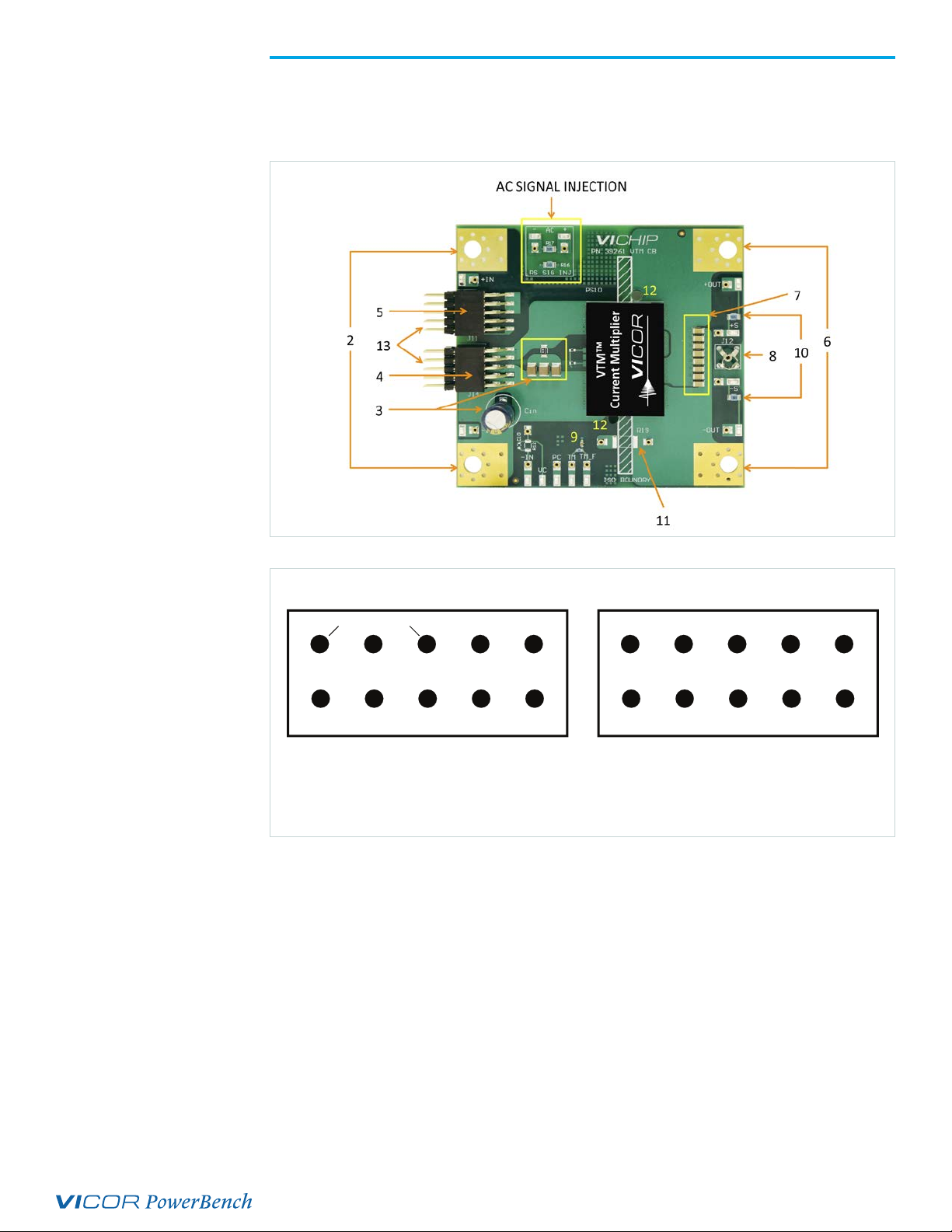
Test Points and Sockets Description
Each test-point socket accepts 0.015 – 0.025 inch diameter leads of solid wires and through-hole
components for use with external circuitry and test equipment. All test points are aligned on the board’s
edge for easy access, measurement and external circuitry connections. Each point is labeled and is
accompanied by an additional adjacent socket.
Reference
Designator
Functional
Name Functional Description
TP20
TP21
+IN
–IN
Input voltage test points provide Kelvin connection to input pins of the VTM™.
Use these test points for measuring the input voltage of the VTM to avoid error
due to interconnect losses.
H20
H21
+IN
–IN Sockets for +IN and –IN test points. Kelvin connected to the VTM input pins.
TP17
TP22
+OUT
–OUT
Output voltage test points provide Kelvin connection to output pins of the
VTM. Use these test points for measuring the output voltage of the VTM to
avoid error due to interconnect losses.
H17
H22
+OUT
–OUT
Sockets for +OUT and –OUT test points. Kelvin connected to the VTM
output pins.
TP12 VC
VC test point provides Kelvin connection to VC pin of the VTM. Can be used
to apply and measure the VC signal with reference to –IN signal. VC is used to
enable the VTM. Apply 14V to VC to enable the VTM, when not using PRM.
H12 VC Socket for VC test point. Kelvin connected to VC pin of the VTM. Aligned with
–IN socket for placing through hole resistor from VC to –IN.
TP10 PC
PC test point provides Kelvin connection to PC pin of the VTM. Can be used
to measure the PC signal with reference to –IN signal. PC can be used to
disable the VTM in the presence of input power. Connecting PC to –IN will
disable the VTM.
H10 PC Socket for PC test point. Kelvin connected to PC pin of the VTM.
TP11 TM TM test point provides Kelvin connection to TM pin of the VTM. Can be used
to measure and monitor the TM signal with reference to –IN signal.
H11 TM Socket for TM test point. Kelvin connected to TM signal of the VTM
TP16 FILTERED
TM
Provides the low noise measurement of TM signal. Output of the TM RC filter
can be measured using this testpoint with reference to –IN.
H15 FILTERED
TM Socket for TP16 test point.
TP13 –IN –IN test point provides Kelvin connection to –IN pin of the VTM. All signals on
input side of the VTM are measured with reference to –IN signal of the VTM.
H13 –IN Socket for –IN test point.
TP15
TP14
+S
–S
Output sense test points provide connection to the output pins of VTM
through local-sense resistors. Routed to connector J11 for use in
differential non-isolated remote-sense circuitry for remote-sense operation of
VTM and PRM™.
H15
H14
+S
–S Sockets for +S and –S test points.
TP18
TP19 AC SIG INJ
Can be used to inject the isolated signal of network analyzer for bode plot
measurement to measure the stability in remote-sense operation using VTM
and PRM
H18
H19 AC SIG INJ Sockets for AC +/– test points.
TP30 IM
IM test point provides the Kelvin connection to IM pin. Can be used to measure
the IM signal of the half VTM. IM can be used to monitor the output current of
the VTM. Available on half-VTM boards only.
H27 IM Socket for IM test point.
Table 1
Test points and
sockets description