Vincotech A1035-H User manual

GPS Receiver A1035-H
A Description of Vincotech’s
GPS Receiver / Smart Antenna Module A1035-H
User’s Manual
Version 1.5
Hardware Revision 01

Revision History
Rev. Date Description
1.0 01-26-09 Release
1.1 02-09-09 Correction of additional solder pad information
1.2 02-18-09 Added nRST information link in signal table; comments on boot se-
lect added
1.3 02-18-09 Added chapter on evaluation kit
1.4 06-30-09 Corrected soldering profile; extended temperature range specifica-
tion with slightly decreased performance below -30°C; corrected
(decreased) current draw figures; added chapter on antenna supply
switch; added hint on “Ephemeris Push”; corrected reel and box
quantities
1.5 12-11-09 New label description (introduced cw50/09); extended minimum con-
figuration; application note on Hibernate Mode extended (use of
ON_OFF pin or Shutdown Command)
mm-dd-yy
V1.5 – Dec-09 User’s Manual Page 2 of 37

Disclaimer
THIS DOCUMENT CONTAINS PROPRIETARY INFORMATION OF VINCOTECH
GMBH. IT MAY NOT BE COPIED OR TRANSMITTED BY ANY MEANS, PASSED
TO OTHERS, OR STORED IN ANY RETRIEVAL SYSTEM OR MEDIA, WITHOUT
PRIOR CONSENT OF VINCOTECH OR ITS AUTHORIZED AGENTS.
THE INFORMATION IN THIS DOCUMENT IS, TO THE BEST OF OUR
KNOWLEDGE, ENTIRELY CORRECT. HOWEVER, VINCOTECH CAN NEITHER
ACCEPT LIABILITY FOR ANY INACCURACIES, OR THE CONSEQUENCES
THEREOF, NOR FOR ANY LIABILITY ARISING FROM THE USE OR
APPLICATION OF ANY CIRCUIT, PRODUCT, OR EXAMPLE SHOWN IN THE
DOCUMENT.
THE PRODUCT (HARD- AND SOFTWARE) DESCRIBED IN THIS DOCUMEN-
TATION IS NOT AUTHORIZED FOR USE IN LIFE SUPPORT DEVICES OR
SYSTEMS WITHOUT THE EXPRESS WRITTEN APPROVAL OF VINCOTECH.
THIS DOCUMENT MAY PROVIDE LINKS TO OTHER WORLD WIDE WEB SITES
OR RESOURCES. BECAUSE VINCOTECH HAS NO CONTROL OVER SUCH
SITES AND RESOURCES, VINCOTECH SHALL NOT BE RESPONSIBLE FOR
THE AVAILABILITY OF SUCH EXTERNAL SITES OR RESOURCES, AND DOES
NOT ENDORSE AND IS NOT RESPONSIBLE OR LIABLE FOR ANY CONTENT,
ADVERTISING, PRODUCTS, OR OTHER MATERIALS ON OR AVAILABLE
FROM SUCH SITES OR RESOURCES. VINCOTECH SHALL NOT BE
RESPONSIBLE OR LIABLE, DIRECTLY OR INDIRECTLY, FOR ANY DAMAGE
OR LOSS CAUSED OR ALLEGED TO BE CAUSED BY OR IN CONNECTION
WITH USE OF OR RELIANCE ON ANY SUCH CONTENT, GOODS OR
SERVICES AVAILABLE ON OR THROUGH ANY SUCH SITE OR RESOURCE.
VINCOTECH RESERVES THE RIGHT TO CHANGE, MODIFY, OR IMPROVE
THIS DOCUMENT OR THE PRODUCT DESCRIBED HEREIN, AS SEEN FIT BY
VINCOTECH WITHOUT FURTHER NOTICE.
V1.5 – Dec-09 User’s Manual Page 3 of 37

Table of Contents
1 Introduction........................................................................................................6
1.1 Label .................................................................................................................6
1.2 Characteristics ..................................................................................................7
1.2.1 GPS Characteristics ................................................................................................... 7
1.2.2 Mechanical Characteristics......................................................................................... 7
1.3 Handling Precautions ........................................................................................ 7
2 Ordering Information.........................................................................................8
2.1 GPS Receiver A1035-H .................................................................................... 8
2.2 Packing .............................................................................................................8
2.3 Additional Equipment ...................................................................................... 10
3 Quick Start........................................................................................................11
3.1 Minimum Configuration ................................................................................... 11
3.2 Antenna...........................................................................................................14
3.3 Serial Port Settings .........................................................................................14
3.4 Improved TTFF ............................................................................................... 14
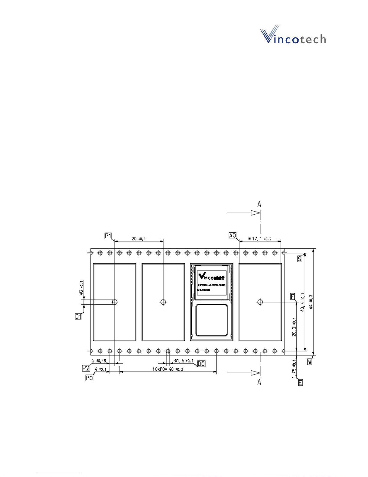
4 Mechanical Outline ..........................................................................................15
4.1 Details Component Side A1035-H .................................................................. 15
4.2 Details Solder Side A1035-H .......................................................................... 16
5 Pin-out Information..........................................................................................17
5.1 Layout A1035-H .............................................................................................. 17
5.2 Description A1035-H Signals .......................................................................... 18
5.3 General Comments ......................................................................................... 19
6 Electrical Characteristics................................................................................20
6.1 Operating Conditions ...................................................................................... 20
6.2 Absolute Maximum Ratings ............................................................................ 20
6.3 DC Electrical Characteristics........................................................................... 21
7 Mounting...........................................................................................................22
7.1 Proposed Footprint for Soldering .................................................................... 22
7.2 Recommended Profile for Reflow Soldering ................................................... 22
8 Use of External Antenna..................................................................................24
8.1 Connection of RF Signal ................................................................................. 24
8.2 External Antenna............................................................................................. 25
8.2.1 Recommended Parameters...................................................................................... 25
8.2.2 Switching External Antenna Supply.......................................................................... 26
8.2.3 Hints ......................................................................................................................... 26
9 Quality and Reliability......................................................................................27
9.1 Environmental Conditions ............................................................................... 27
9.2 Product Qualification ....................................................................................... 27
9.3 Production Test............................................................................................... 27
V1.5 – Dec-09 User’s Manual Page 4 of 37

10 Application and Hints....................................................................................28
10.1 Minimum Configuration ................................................................................. 28
10.2 External Antenna Status Adaptation ............................................................. 28
10.2.1 External Antenna Sensor........................................................................................ 28
10.2.2 External Antenna Sensor with Current Limiter ....................................................... 29
10.3 VANT Pin (antenna voltage input pin) ........................................................... 30
10.4 1PPS Pin (1 pulse per second pin) ............................................................... 30
10.5 Reset Signal.................................................................................................. 31
10.5.1 Internal Reset Circuit .............................................................................................. 31
10.5.2 External Reset Circuit............................................................................................. 31
10.6 Battery Back-up............................................................................................. 32
10.7 Push-to-Fix Mode.......................................................................................... 33
10.8 Hibernate Mode............................................................................................. 33
10.8.1 Entering Hibernate Mode with ON_OFF Pin .......................................................... 33
10.8.2 Entering Hibernate Mode with Shutdown Command.............................................. 33
11 Evaluation Kit EVA1035-H.............................................................................34
12 Related Information .......................................................................................35
12.1 Contact.......................................................................................................... 35
12.2 Related Documents....................................................................................... 35
12.3 Related Tools ................................................................................................ 35
13 List of Figures ................................................................................................36
14 List of Tables..................................................................................................37
V1.5 – Dec-09 User’s Manual Page 5 of 37

1 Introduction
Vincotech’s GPS receiver module / smart antenna A1035-H is a highly integrated
GPS antenna receiver module based on the technology of the GPS receiver mod-
ule A1084 and a ceramic GPS patch antenna. Like on the A1084-A an RF switch is
integrated on the module allowing changing of RF input from the on-module an-
tenna to an external antenna. The module is capable of receiving signals from up to
20 GPS satellites and transferring them into position and timing information that can
be read over a serial port. Small size and high-end GPS functionality are combined
at low power consumption:
•Operable at 3.3V / 24mA (typ.) @ 1fix per second
•UART interface at CMOS level
•Small form factor of 30.48 x 16.51 mm² (1.2” x 0.65”)
•Supported temperature range: -40°C to +85°C
•Single-sided SMT component, for reflow soldering
•RoHS compliant, lead-free
•Tape & reel packaging
•Excellent antenna support
oOn-module patch antenna
oAntenna input for direct connection of external active antenna
oRF switch to select between antennas
The receiver / smart antenna module is available as an off-the-shelf component,
100% tested and shipped in tape-and-reel.
1.1 Label
The A1035-H label (size: 9.5 x 9.5 mm²) contains the following information:
Vincotech
A1035-Hsss-tt-rr
YK/wwyy
Hardware
rr: hardware revision
Software
sss: software version
tt: software release
Location and date code
YK: Bicske / Hungary
ww: production week
yy: production year
: Green, if OK
General description Example
Vincotech
A1035-H350-02-01
YK/0110
Vincotech
A1035-Hsss-tt-rr
YK/wwyy
Hardware
rr: hardware revision
Software
sss: software version
tt: software release
Location and date code
YK: Bicske / Hungary
ww: production week
yy: production year
: Green, if OK
General description Example
Vincotech
A1035-H350-02-01
YK/0110
Figure 1: A1035-H label
The data matrix code holds a 6-digit lot and 4-digit serial number. The label is
placed on the shield of the module.
V1.5 – Dec-09 User’s Manual Page 6 of 37

1.2 Characteristics
The module is characterized by the following parameters.
1.2.1 GPS Characteristics
Channels 20, parallel tracking
Correlators 200,000 plus
Frequency L1 (= 1,575 MHz)
Tracking Sensitivity
External active antenna
On-module antenna
-159 dBm
-157 dBm
Horizontal Position Accuracy Stand alone < 2.5 m CEP (SA off)
Position Accuracy Stand alone < 10 m CEP (SA off)
Obscuration recovery (1) 0.1 s
Hot start (2) < 1 s
Warm (3) < 32 s
Time To First Fix – TTFF
(theoretical minimum values;
values in real world may differ)
Cold (4) < 35 s
Table 1: A1035-H GPS characteristics
(1) The calibrated clock of the receiver has not stopped, thus it knows precise time (to the µs level).
(2) The receiver has estimates of time/date/position and valid almanac and ephemeris data.
(3) The receiver has estimates of time/date/position and recent almanac.
(4) The receiver has no estimate of time/date/position, and no recent almanac.
Note: Performance (sensitivity and TTFF) might slightly decrease below -30°C.
1.2.2 Mechanical Characteristics
A1035-H Mechanical dimensions
Length
Width
Height
30.48 mm, 1.2”
16.51 mm, 0.65”
5.00 mm, 0.2”
A1035-H Weight 4.0 g, 0.14 oz
Table 2: A1035-H dimensions and weight
1.3 Handling Precautions
The GPS receiver module A1035-H is sensitive to electrostatic discharge (ESD).
Please handle with appropriate care.
V1.5 – Dec-09 User’s Manual Page 7 of 37

2 Ordering Information
2.1 GPS Receiver A1035-H
The order number is built as follows:
•V23993-A1035-Hxxx
V23993 stands for Vincotech wireless and communication products, A1035-H for
the A1035-H module. The “xxx” reflects the current firmware version. If no firmware
version is noted in an order, the latest version will be provided.
2.2 Packing
The A1035-H GPS modules come in a tape and reel package suitable for pick and
place machines.
Figure 2: A1035-H tape specifications (1)
V1.5 – Dec-09 User’s Manual Page 8 of 37

Figure 3: A1035-H tape specifications (2)
Figure 4: A1035-H tape specifications (3)
One complete reel holds 700 A1035-H modules.
One box holds two reels, so a total of 1400 A1035-H modules.
V1.5 – Dec-09 User’s Manual Page 9 of 37

2.3 Additional Equipment
V23993-EVA1035-H Evaluation Kit (including one module A1035-H)
Table 3: Additional equipment
A detailed description of the EVA1035-H Evaluation Kit can be found in the appro-
priate manual.
V1.5 – Dec-09 User’s Manual Page 10 of 37

3 Quick Start
In order to allow an easy and quick start with the A1035-H module, this chapter
provides a short overview on the important steps to be taken to receive NMEA
messages with position information on a serial port.
3.1 Minimum Configuration
The following pictures show two versions of recommended minimum configurations
for NMEA output and commands sent and received via an RS232 interface based
on the GPS antenna module A1035-H using the on-module antenna. While the first
version foresees that Vcc is applied continuously, the second version assumes a
separate back-up battery. In order to go to Hibernate Mode (low power mode) the
two configurations use different approaches. The first version requires toggling of
the ON_OFF pin and continued supply of Vcc. With the second version a shutdown
command is required; then after a further delay Vcc can be switched off completely.
In both cases the current drawn will drop drastically. See also chapter “10.8
Hibernate Mode”.
ON_OFF
Tx
Rx
3.3V
GND
Shown from top without lid; pads shown for better understanding
A1035-H
GSC3f/LPx
serial
ON_OFF
Tx
Rx
3.3V
GND
Shown from top without lid; pads shown for better understanding
A1035-H
GSC3f/LPx
serial
Figure 5: Minimum configuration A1035-H with continued Vcc supply
Remarks:
•Use separate ground plane for antenna ground.
•External antenna input impedance is 50 Ω. Match as close as possible.
•Maximum allowed external antenna current is 50 mA. Consider a current lim-
iter.
•Supply Vcc continuously, use toggling of ON_OFF to switch between normal
operation and hibernate mode
V1.5 – Dec-09 User’s Manual Page 11 of 37

Vbak
A B
Vbak
GND
Vbak
GND
Supercap
Battery
C6 +
+
Back-up supply options
(A) Supercap, charged through GPS module
(B) Primary cell, decoupled with diode
NSR0310
Tx
Rx
3.3V
GND
Shown from top without lid; pads shown for better understanding
A1035-H
GSC3f/LPx
serial
Vbak
A B
Vbak
GND
Vbak
GND
Supercap
Battery
C6 +
+
Back-up supply options
(A) Supercap, charged through GPS module
(B) Primary cell, decoupled with diode
NSR0310
Tx
Rx
3.3V
GND
Shown from top without lid; pads shown for better understanding
A1035-H
GSC3f/LPx
serial
Figure 6: Minimum configuration A1035-H with Vbak
Remarks:
•Use separate ground plane for antenna ground.
•External antenna input impedance is 50 Ω. Match as close as possible.
•Maximum allowed external antenna current is 50 mA. Consider a current lim-
iter.
•A battery back-up circuit for the RTC (Real Time Clock) should be consid-
ered (see chapter: “10.6 Battery Back-up”)
•Send shutdown command along with a further delay (2s) before switching
Vcc off
V1.5 – Dec-09 User’s Manual Page 12 of 37

For completeness the following pictures show the use of an RS232 level shifter.
GND
1
2
3
4
5
6
7
8
9
C1
0.1µF
C2
0.1µF
C3
0.1µF
C4
0.1µF
C5
0.1µF
RS232 Level Shifter
RS232 Out
DB9 female
3.3V
Vcc
GND
T1O
R1I
R1O
T1I
T2I
R2O
C1+
V+
C1-
C2+
C2-
V-
T2O
R2I
MAX3232
Tx
Rx
GND
1
2
3
4
5
6
7
8
9
C1
0.1µF
C2
0.1µF
C3
0.1µF
C4
0.1µF
C5
0.1µF
RS232 Level Shifter
RS232 Out
DB9 female
3.3V
Vcc
GND
T1O
R1I
R1O
T1I
T2I
R2O
C1+
V+
C1-
C2+
C2-
V-
T2O
R2I
MAX3232
Tx
Rx
Figure 7: RS232 level shifter for minimum configurations
Remarks:
•Place C1 to C5 (here: 0.1µF) close to MAX3232. For capacity values see
datasheet of actual component used.
•Use 3.3V level shifter (MAX3232 or equivalent).
V1.5 – Dec-09 User’s Manual Page 13 of 37

3.2 Antenna
Although the A1035-H offers an on-module antenna, an additional external active
antenna can be used. Switching between both antennas is done via pin 12 (see
also “5.2 Description A1035-H Signals”). It is recommended to use an active GPS
antenna with supply voltage of 3 to 5 VDC and a current draw of 50 mA maximum.
The quality of the GPS antenna chosen is of paramount importance to the overall
sensitivity of the GPS system. An active antenna should have a gain ≥20 dB and a
noise figure ≤1.5 dB, which applies to more than 95% of the active antennas avail-
able in the market.
3.3 Serial Port Settings
The default configuration within the custom-specific GPS firmware is:
•Serial 0 (NMEA) 4800 baud, 8 data bits, no parity, 1 stop bit, no flow control
3.4 Improved TTFF
In order to improve the TTFF (Time To First Fix), it is recommended to support the
RTC and SRAM with a back-up power when no system power is available.
Furthermore, starting with FW revision 3.5.0 “Ephemeris Push” is supported. Please
see according application note!
V1.5 – Dec-09 User’s Manual Page 14 of 37

4 Mechanical Outline
4.1 Details Component Side A1035-H
29.845 (1.175)
12.70 (.50)
11.43 (.45)
10.16 (.40)
8.89 (.35)
7.62 (.30)
6.35 (.25)
5.08 (.20)
3.81 (.15)
2.54 (.10)
1.27 (.05)
0.00 (.00)
0.00 (.00)
29.845 (1.175)
16.52 (.65)
15.24 (.60)
13.97 (.55)
7.62 (.30)
6.35 (.25)
5.08 (.20)
3.81 (.15)
2.54 (.10)
1.27 (.05)
16.51 (0.65)
30.48 (1.20) 29.845 (1.175)
12.70 (.50)
11.43 (.45)
10.16 (.40)
8.89 (.35)
7.62 (.30)
6.35 (.25)
5.08 (.20)
3.81 (.15)
2.54 (.10)
1.27 (.05)
0.00 (.00)
0.00 (.00)
29.845 (1.175)
16.52 (.65)
15.24 (.60)
13.97 (.55)
7.62 (.30)
6.35 (.25)
5.08 (.20)
3.81 (.15)
2.54 (.10)
1.27 (.05)
16.51 (0.65)
30.48 (1.20)
All dimensions in [mm] / [(inches)]
Figure 8: Mechanical outline component side A1035-H
V1.5 – Dec-09 User’s Manual Page 15 of 37

4.2 Details Solder Side A1035-H
3.81 (.15)
16.51 (0.65)
30.48 (1.2)
1.27 (.05)
29.845 (1.175)
13.97 (.55)
1.27 (.05)
2.54 (.10)
2.54 (.10)
1.27 (.05)
1.0 x 0.8
1.27 x 1.27
3.81 (.15)
3.81 (.15)3.81 (.15)
3.81 (.15)
16.51 (0.65)
30.48 (1.2)
1.27 (.05)
29.845 (1.175)
13.97 (.55)
1.27 (.05)
2.54 (.10)
2.54 (.10)
1.27 (.05)
1.0 x 0.8
1.27 x 1.27
3.81 (.15)
3.81 (.15)3.81 (.15)
Solder pad size (outer pads): 1.0 x 0.8
Solder pad size (inner pads): 1.27 x 1.27
All dimensions in [mm] / [(inches)]
Figure 9: Mechanical outline solder side A1035-H
V1.5 – Dec-09 User’s Manual Page 16 of 37

5 Pin-out Information
5.1 Layout A1035-H
Figure 10: Pin-out information (bottom view) A1035-H
V1.5 – Dec-09 User’s Manual Page 17 of 37

5.2 Description A1035-H Signals
Pin Symbol Function Description
1 nRST Input Reset input (open / HIGH – no reset, LOW - reset);
see “10.5 Reset Signal”
2 BOOTSEL Input Special boot mode – leave open for normal operation;
(HIGH – boot loader active)
3 Vcc Power Supply 3.0 – 3.6 VDC (power supply)
4 RFPWUP Output Status of analog section (LOW = OFF, HIGH = ON) – can
be used to switch external antenna supply (see also
GPIO0)
5 GPIO 15 Reserved Reserved – leave open
6 GND Power Supply Ground (power supply)
7 ANT_GND RF GND Antenna Ground, do not connect to GROUND, connect to
antenna shield
8 ANT_EXT Antenna Input Antenna signal / Z=50 Ohm (external active antenna in-
put)
9 VANT Power supply Power supply antenna – provide according voltage (up to
5.0 VDC) - VANT feeds Pin 8 ANT_EXT
10 DNC Do not connect
to a signal
Mechanical fixture only
11 DNC Do not connect
to a signal
Mechanical fixture only
12 ANT_SW Input Antenna switch (LOW or open = internal antenna, HIGH
= external antenna)
13 GPIO 0 Output Antenna supply status – if LOW external antenna supply volt-
age can be switched off (this is not done internally!)
14 Vbak Power Supply Back-up pin of module for “super cap” or battery (see
below)
15 1PPS Output 1PPS (pulse per second) output
16 nWAKEUP Output Status of digital section (Low = ON, High = OFF)
Open Drain with internal pull-up (100k), can not source
current!
17 ON_OFF Input - ON_OFF, used in PTF mode to request a fix by toggling
from LOW to HIGH
- ON_OFF, used to switch to hibernate mode and back
- leave open if not used
18 RX1 Input Serial input 1 – unused in current firmware (leave open)
19 TX1 Output Serial output 1 – unused in current firmware (leave open)
20 TX0 Output Serial output 0, NMEA out
21 RX0 Input Serial input 0, NMEA in
Table 4: Pin description A1035-H
V1.5 – Dec-09 User’s Manual Page 18 of 37

5.3 General Comments
The following comments should be considered for a design with and use of the
module:
•Standard configuration of serial port (standard GPS software):
Serial 0 (NMEA) 4800 baud, 8 data bits, no parity, 1 stop bit, no flow control
•External antenna (Antenna connected to Antenna Pin)
Use ground pin 7 close to the antenna input for RF ground.
V1.5 – Dec-09 User’s Manual Page 19 of 37

6 Electrical Characteristics
6.1 Operating Conditions
Pin Description Min Typical Max
Vbak 1.8V 3.6V14
Standby Current (4) 20µA
Vcc 3.0V 3.3V 3.6V
Peak Acquisition Current (1) 36mA
Average Acquisition Current (2) 31mA
3
Tracking Current (3) 26mA
Table 5: A1035-H electrical characteristics
(1) Peak acquisition current is characterized by millisecond bursts above average acquisition cur-
rent
(2) Average current is typically only the first two seconds of TTFF
(3) Tracking current typically includes tracking and the post acquisition portion of TTFF
(4) During standby state: RTC block and core powered on and clock off.
6.2 Absolute Maximum Ratings
Symbol Parameter Min Max Unit
Vcc Power supply -0.3 +3.6 V
Vin Voltage to any pin -0.3 +3.6 V
Iov Input current on any pin -10 10 mA
Itdv Absolute sum of all input currents during overload condition 200 mA
Tst Storage temperature -55 125 °C
Vant Antenna supply voltage 0 5.5 V
Iant Antenna supply current 0 50 mA
Table 6: Absolute maximum ratings
Stresses beyond those listed under “Absolute Maximum Ratings” may cause per-
manent damage to the device. This is a stress rating only. Functional operation of
the device at these or any other conditions beyond those indicated in the opera-
tional sections of this specification is not implied. Exposure to absolute maximum
rating conditions for extended periods may affect device reliability.
V1.5 – Dec-09 User’s Manual Page 20 of 37
Table of contents