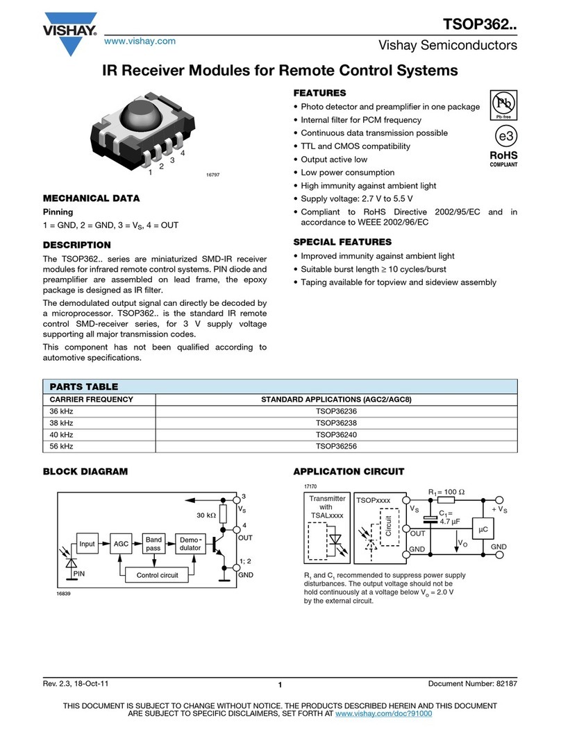
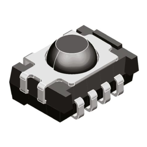
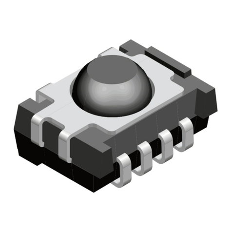
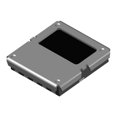
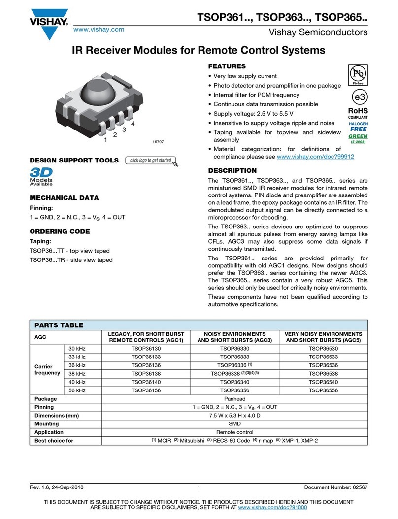
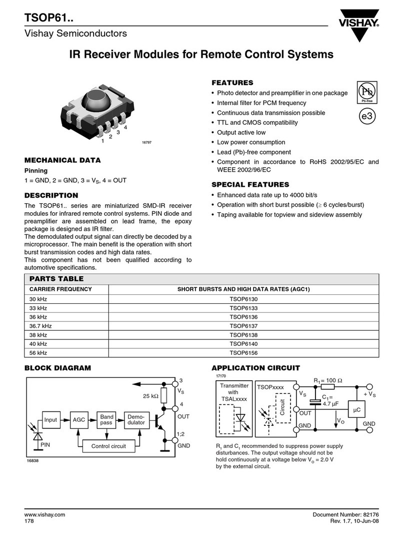
Vishay TSOP373 Series User manual

TSOP373.., TSOP375..
www.vishay.com Vishay Semiconductors
Rev. 1.5, 25-Feb-14 1Document Number: 82446
THIS DOCUMENT IS SUBJECT TO CHANGE WITHOUT NOTICE. THE PRODUCTS DESCRIBED HEREIN AND THIS DOCUMENT
ARE SUBJECT TO SPECIFIC DISCLAIMERS, SET FORTH AT www.vishay.com/doc?91000
IR Receiver Modules for Remote Control Systems
ORDERING CODE
Taping:
TSOP37...TT - top view taped
TSOP37...TR - side view taped
FEATURES
• Very low supply current
• Photo detectors and preamplifier in one package
• Internal filter for PCM frequency
• Supply voltage: 2.5 V to 5.5 V
• Improved immunity against ambient light
• Insensitive to supply voltage ripple and noise
• Material categorization:
For definitions of compliance please see
www.vishay.com/doc?99912
DESCRIPTION
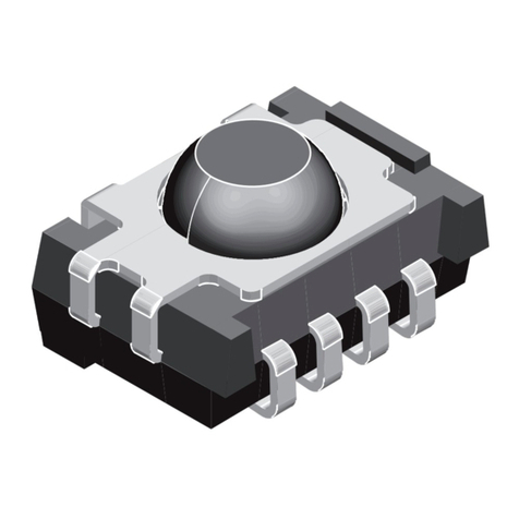
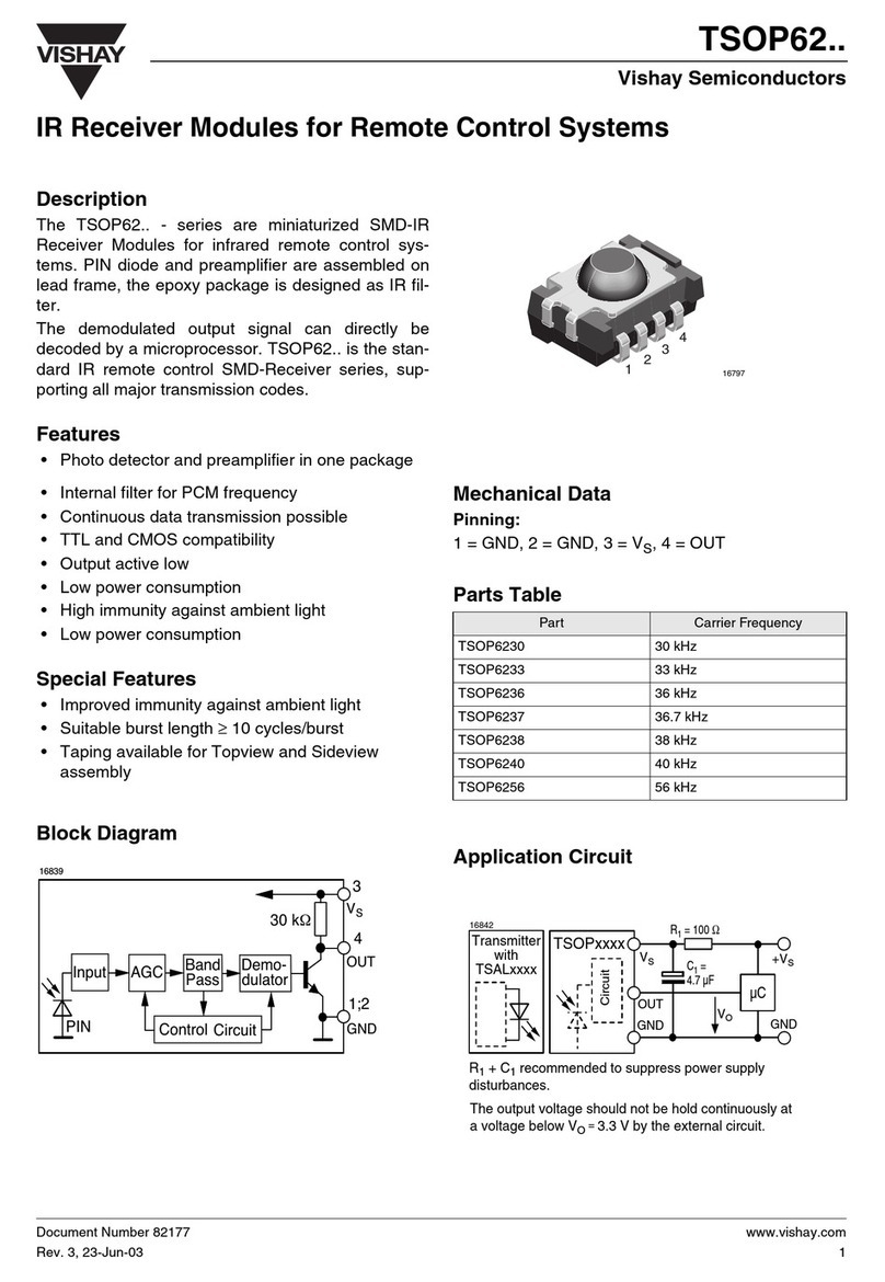
The TSOP373.., TSOP375.. series are miniaturized receiver
modules for infrared remote control systems. A PIN diode
and a preamplifier are assembled on a PCB, the epoxy lens
cap is designed as an IR filter.
The demodulated output signal can be directly connected to
a microprocessor for decoding. The TSOP373.. is optimized
to better suppress spurious pulses from energy saving
lamps. The TSOP375.. has an excellent noise suppression.
It is immune to dimmed LCD backlighting and any
fluorescent lamps. AGC3 and AGC5 may also suppress
some data signals in case of continuous transmission.
This component has not been qualified according to
automotive specifications.
BLOCK DIAGRAM APPLICATION CIRCUIT
22531-1
PARTS TABLE
AGC NOISY ENVIRONMENTS
AND SHORT BURSTS (AGC3)
VERY NOISY ENVIRONMENTS
AND SHORT BURSTS (AGC5)
Carrier
frequency
36 kHz TSOP37336 (1)(2) TSOP37536 (1)(2)
38 kHz TSOP37338 (3)(4)(5)(6) TSOP37538 (3)(4)(5)
40 kHz TSOP37340 TSOP37540
56 kHz TSOP37356 TSOP37556
Package Belobog
Pinning 1 = OUT, 2, 3, 6, 7, 8 = GND, 4, 5 = VS
Dimensions (mm) 3.95 W x 3.95 H x 0.8 D
Mounting SMD
Application Remote control
Best remote control code (1) MCIR (2) RCMM (3) Mitsubishi (4) RECS-80 Code (5) r-map (6) XMP-1, XMP-2
30 kΩ
VS
OUT
Demo-
GND
pass
AGCInput
PIN
Band dulator
Control circuit
4, 5
1
2, 3,
6, 7, 8
20445-5
C
1
IR receiver
GND
Circuit
µC
R
1
+ V
S
GND
Transmitter
with
TSALxxxx V
S
V
O
17170_5
OUT
R1and C1are recommended for protection against EOS.
Components should be in the range of 33 Ω< R1< 1 kΩ,
C1> 0.1 µF.
TSOP373.., TSOP375..
www.vishay.com Vishay Semiconductors
Rev. 1.5, 25-Feb-14 2Document Number: 82446
THIS DOCUMENT IS SUBJECT TO CHANGE WITHOUT NOTICE. THE PRODUCTS DESCRIBED HEREIN AND THIS DOCUMENT
ARE SUBJECT TO SPECIFIC DISCLAIMERS, SET FORTH AT www.vishay.com/doc?91000
Note
• Stresses beyond those listed under “Absolute Maximum Ratings” may cause permanent damage to the device. This is a stress rating only
and functional operation of the device at these or any other conditions beyond those indicated in the operational sections of this specification
is not implied. Exposure to absolute maximum rating conditions for extended periods may affect the device reliability.
TYPICAL CHARACTERISTICS (Tamb = 25 °C, unless otherwise specified)
Fig. 1 - Output Function Fig. 2 - Output Pulse Width vs. Irradiance
ABSOLUTE MAXIMUM RATINGS
PARAMETER TEST CONDITION SYMBOL VALUE UNIT
Supply voltage VS-0.3 to +6 V
Supply current IS3mA
Output voltage VO-0.3 to (VS+ 0.3) V
Output current IO5mA
Junction temperature Tj100 °C
Storage temperature range Tstg -25 to +85 °C
Operating temperature range Tamb -25 to +85 °C
Power consumption Tamb ≤85 °C Ptot 10 mW
ELECTRICAL AND OPTICAL CHARACTERISTICS (Tamb = 25 °C, unless otherwise specified)
PARAMETER TEST CONDITION SYMBOL MIN. TYP. MAX. UNIT
Supply voltage VS2.5 5.5 V
Supply current VS= 3.3 V, Ev= 0 ISD 0.27 0.35 0.45 mA
Ev= 40 klx, sunlight ISH 0.45 mA
Transmission distance Ev= 0, IR diode TSAL6200,
IF= 200 mA, test signal see fig. 1 d45m
Output voltage low IOSL = 0.5 mA, Ee= 0.7 mW/m2,
test signal see fig. 1 VOSL 100 mV
Minimum irradiance
Pulse width tolerance:
tpi - 5/fo< tpo < tpi + 6/fo,
test signal see fig. 1
Ee min. 0.12 0.25 mW/m2
Maximum irradiance tpi - 5/fo< tpo < tpi + 6/fo,
test signal see fig. 1 Ee max. 30 W/m2
Directivity Angle of half transmission
distance ϕ1/2 ± 75 deg
Ee
T
tpi *) t
VO
VOH
VOL tpo 2) t
14337
Optical Test Signal
(IR diode TSAL6200, IF= 0.4 A, N = 6 pulses, f = f0, t = 10 ms)
Output Signal
td1)
1) 3/f0< td< 9/f0
2) tpi - 4/f0< tpo < tpi + 6/f0
*) tpi ≥6/f0is recommended for optimal function
0
0.1
0.2
0.3
0.4
0.5
0.6
0.7
0.8
0.9
1.0
0.1 1 10 102103104105
E
e
- Irradiance (mW/m
2
)
t
po
- Output Pulse Width (ms)
20752
Input Burst Length
λ= 950 nm,
Optical Test Signal, Fig.1
Output Pulse Width

TSOP373.., TSOP375..
www.vishay.com Vishay Semiconductors
Rev. 1.5, 25-Feb-14 3Document Number: 82446
THIS DOCUMENT IS SUBJECT TO CHANGE WITHOUT NOTICE. THE PRODUCTS DESCRIBED HEREIN AND THIS DOCUMENT
ARE SUBJECT TO SPECIFIC DISCLAIMERS, SET FORTH AT www.vishay.com/doc?91000
Fig. 3 - Output Function
Fig. 4 - Output Pulse Diagram
Fig. 5 - Frequency Dependance of Responsivity
Fig. 6 - Sensitivity in Bright Ambient
Fig. 7 - Sensitivity vs. Supply Voltage Disturbances
Fig. 8 - Max. Envelope Duty Cycle vs. Burst Length
E
e
t
V
O
V
OH
V
OL
t
600 µs 600 µs
t = 60 ms
t
on
t
off
94 8134
Optical Test Signal
Output Signal, (see fig. 4)
0
0.1
0.2
0.3
0.4
0.5
0.6
0.7
0.8
0.1 1 10 100 1000 10 000
E
e
- Irradiance (mW/m
2
)
T
on
, T
off
- Output Pulse Width (ms)
20759
λ= 950 nm,
Optical Test Signal, Fig. 3
T
on
T
off
0.0
0.2
0.4
0.6
0.8
1.0
1.2
0.7 0.9 1.1 1.3
f/f0- Relative Frequency16925
f = f0± 5 %
Δf(3 dB) = f0/10
E /E - Rel. Responsivity
e min. e
0
0.5
1
1.5
2
2.5
3
3.5
4
0.01 0.1 1 10 100
Ee- Ambient DC Irradiance (W/m2)
Ee min. - Threshold Irradiance (mW/m2)
Correlation with Ambient Light Sources:
10 W/m2= 1.4 kLx (Std. illum. A, T = 2855 K)
10 W/m2= 8.2 kLx (Daylight, T = 5900 K)
Wavelength of Ambient
Illumination:
λ
= 950 nm
20757
0
0.1
0.2
0.3
0.4
0.5
0.6
0.7
0.8
0.9
1.0
1 10 100 1000
VsRMS - AC Voltage on DC Supply Voltage (mV)
20753
Ee min. - Threshold Irradiance (mW/m2)
f = fo
f = 20 kHz
f = 30 kHz
f = 100 Hz
f = 10 kHz
0
0.1
0.2
0.3
0.4
0.5
0.6
0.7
0.8
0.9
1
0 20406080100120
Burst Length (number of cycles/burst)
Max. Envelope Duty Cycle
f = 38 kHz, Ee= 2 mW/m²
TSOP375..
TSOP373..

TSOP373.., TSOP375..
www.vishay.com Vishay Semiconductors
Rev. 1.5, 25-Feb-14 4Document Number: 82446
THIS DOCUMENT IS SUBJECT TO CHANGE WITHOUT NOTICE. THE PRODUCTS DESCRIBED HEREIN AND THIS DOCUMENT
ARE SUBJECT TO SPECIFIC DISCLAIMERS, SET FORTH AT www.vishay.com/doc?91000
Fig. 9 - Sensitivity vs. Ambient Temperature
Fig. 10 - Relative Spectral Sensitivity vs. Wavelength
Fig. 11 - Directivity
Fig. 12 - Sensitivity vs. Supply Voltage
0
0.05
0.10
0.15
0.20
0.25
0.30
-30 -10 10 30 50 70 90
Ee min. - Threshold Irradiance (mW/m2)
Tamb - Ambient Temperature (°C)
0
0.1
0.2
0.3
0.4
0.5
0.6
0.7
0.8
0.9
1.0
750 800 850 900 950 1000 1050 1150
λ- Wavelength (nm)
S(λ)rel - Relative Spectral Sensitivity
1100
0.1 0.3 0.5 0.7 0.9
80°
70°
60°
50°
40°
30°
20°
10°
0°
-10°
-20°
-30°
-40°
-50°
-60°
-70°
-80°
21947
0.00
0.05
0.10
0.15
0.20
0.25
0.30
1 2 3 4 5
E
e min.
- Sensitivity (mW/m
2
)
V
S
- Supply Voltage (V)

TSOP373.., TSOP375..
www.vishay.com Vishay Semiconductors
Rev. 1.5, 25-Feb-14 5Document Number: 82446
THIS DOCUMENT IS SUBJECT TO CHANGE WITHOUT NOTICE. THE PRODUCTS DESCRIBED HEREIN AND THIS DOCUMENT
ARE SUBJECT TO SPECIFIC DISCLAIMERS, SET FORTH AT www.vishay.com/doc?91000
SUITABLE DATA FORMAT
The TSOP373.., TSOP375.. series is designed to suppress
spurious output pulses due to noise or disturbance signals.
The devices can distinguish data signals from noise due to
differences in frequency, burst length, and envelope duty
cycle. The data signal should be close to the device’s
band-pass center frequency (e.g. 38 kHz) and fulfill the
conditions in the table below.
When a data signal is applied to the TSOP373.., TSOP375..
in the presence of a disturbance, the sensitivity of the
receiver is automatically reduced by the AGC to insure that
no spurious pulses are present at the receiver’s output.
Some examples which are suppressed are:
• DC light (e.g. from tungsten bulbs sunlight)
• Continuous signals at any frequency
• Strongly or weakly modulated patterns from fluorescent
lamps with electronic ballasts (see figure 12 or figure 13)
Fig. 13 - IR Signal from Fluorescent Lamp
with Low Modulation
Fig. 14 - IR Signal from Fluorescent Lamp
with High Modulation
Notes
• For data formats with long bursts (more than 10 carrier cycles) please see the datasheet for TSOP372.., TSOP374.. .
• Best choice of AGC for some popular IR-codes:
-TSOP37336: MCIR, RCMM
- TSOP37538: Mitsubishi, RECS-80 Code
-TSOP37338: XMP-1, XMP-2, r-map
0101520
Time (ms)
16920
IR Signal
5
0101520
Time (ms)
16921
IR Signal
5
TSOP373.. TSOP375..
Minimum burst length 6 cycles/burst 6 cycles/burst
After each burst of length
a minimum gap time is required of
6 to 35 cycles
≥10 cycles
6 to 24 cycles
≥10 cycles
For bursts greater than
a minimum gap time in the data
stream is needed of
35 cycles
> 6 x burst length
24 cycles
> 25 ms
Maximum number of continuous
short bursts/second 2000 2000
MCIR code preferred yes
RCMM code preferred yes
XMP-1, XMP-2 code preferred yes
Suppression of interference from
fluorescent lamps
Even critical disturbance patterns are suppressed
(example: signal pattern of fig. 12 and fig. 13)
Even critical disturbance patterns are suppressed
(example: signal pattern of fig. 12 and fig. 13)

TSOP373.., TSOP375..
www.vishay.com Vishay Semiconductors
Rev. 1.5, 25-Feb-14 6Document Number: 82446
THIS DOCUMENT IS SUBJECT TO CHANGE WITHOUT NOTICE. THE PRODUCTS DESCRIBED HEREIN AND THIS DOCUMENT
ARE SUBJECT TO SPECIFIC DISCLAIMERS, SET FORTH AT www.vishay.com/doc?91000
PACKAGE DIMENSIONS in millimeters
0.8
0.15
3.95
3.95
(2.75)
0.55
(0.95)
0.55
(1.8)
Pinning from Topview
GND
GND
Out
Vs
(Vs)
(GND)
(GND) (GND)
0.75± 0.05
4 x 0.75 = 3
0.35± 0.05
(8 x)
1.5
3
(0.3)
(0.3)
(0.3)
(0.7)
(1.9)
(3.4)
Not indicated tolerances ± 0.1
specifications
according to DIN
technical drawings
All dimensions in mm
Drawing-No.: 6.550-5315.01-4
Issue: 2; 12.02.14
marking area
Drawing refers to following types: TSOP37... / TSOP57...
Proposed pad layout from
component side
(dim. for reference only)
(3.95)
(3.95)
(0.35)
(0.8)
(2.75)
(3)
(4 x)
(4x)
1 2 3 4 5
8 7 6
0.475
(0.4)
Pin 1 Identification
optically effective area
(1)
(1)
(2)
(2) (2) (2)
(2) Pins connected internally.
It is not necessary to
connect externally.
(1)
(1)

TSOP373.., TSOP375..
www.vishay.com Vishay Semiconductors
Rev. 1.5, 25-Feb-14 7Document Number: 82446
THIS DOCUMENT IS SUBJECT TO CHANGE WITHOUT NOTICE. THE PRODUCTS DESCRIBED HEREIN AND THIS DOCUMENT
ARE SUBJECT TO SPECIFIC DISCLAIMERS, SET FORTH AT www.vishay.com/doc?91000
ASSEMBLY INSTRUCTIONS
Reflow Soldering
• Reflow soldering must be done within 168 h while stored
under a max. temperature of 30 °C, 60 % RH after
opening the dry pack envelope
• Set the furnace temperatures for pre-heating and heating
in accordance with the reflow temperature profile as
shown in the diagram. Exercise extreme care to keep the
maximum temperature below 260 °C. The temperature
shown in the profile means the temperature at the device
surface. Since there is a temperature difference between
the component and the circuit board, it should be verified
that the temperature of the device is accurately being
measured
• Handling after reflow should be done only after the work
surface has been cooled off
Manual Soldering
• Use a soldering iron of 25 W or less. Adjust the
temperature of the soldering iron below 300 °C
• Finish soldering within 3 s
• Handle products only after the temperature has cooled off
VISHAY LEAD (Pb)-FREE REFLOW SOLDER PROFILE
Note
(1) MOQ: minimum order quantity
ORDERING INFORMATION
ORDERING CODE PACKAGING VOLUME (1) REMARKS
TSOP37..TT1 Tape and reel MOQ: 1800 pcs 3.95 mm x 3.95 mm x 0.75 mm
TSOP37..TT2 MOQ: 7000 pcs
0
50
100
150
200
250
300
0 50 100 150 200 250 300
t (s)
T (°C)
255 °C
240 °C
245 °
C
max. 260 °C
max. 120 s max. 100 s
217 °C
max. 20 s
max. Ramp Up 3 °C/s max. Ramp Down 6 °C/s
max. 2 cycles allowed
19800

TSOP373.., TSOP375..
www.vishay.com Vishay Semiconductors
Rev. 1.5, 25-Feb-14 8Document Number: 82446
THIS DOCUMENT IS SUBJECT TO CHANGE WITHOUT NOTICE. THE PRODUCTS DESCRIBED HEREIN AND THIS DOCUMENT
ARE SUBJECT TO SPECIFIC DISCLAIMERS, SET FORTH AT www.vishay.com/doc?91000
TAPING VERSION TSOP37... DIMENSIONS in millimeters
Leader and trailer tape:
Partsmounted
Empty trailer 200 mm min.
Empty leader 400 mm min.
Direction of pulling out
Unreel direction
Ø 60 min.
Ø Y
2 ± 0.5
Label posted here
coming out from reel
Tape position
(12.4)
18.4 max.
Ø 13 ± 0.2
Ø 21 ± 0.8
100 mm min. with cover tape
X 2:1
Tape and reel dimensions:
(2)
(1.75)
(5.5)
12 ± 0.3
(8) (4)
(Ø 1.5)
(0.3)
Reel size "Y"
TT1 Ø 180 ± 2 = 1800 pcs.
TT2 Ø 330 ± 2 = 7000 pcs.
(1.2)
Technical drawings
according to DIN
specications
Not indicated tolerances± 0.1Drawing-No.: 9.700-5347.01-4
Issue: 1; 14.11.11

TSOP373.., TSOP375..
www.vishay.com Vishay Semiconductors
Rev. 1.5, 25-Feb-14 9Document Number: 82446
THIS DOCUMENT IS SUBJECT TO CHANGE WITHOUT NOTICE. THE PRODUCTS DESCRIBED HEREIN AND THIS DOCUMENT
ARE SUBJECT TO SPECIFIC DISCLAIMERS, SET FORTH AT www.vishay.com/doc?91000
LABEL
Standard bar code labels for finished goods
The standard bar code labels are product labels and used
for identification of goods. The finished goods are packed in
final packing area. The standard packing units are labeled
with standard bar code labels before transported as finished
goods to warehouses. The labels are on each packing unit
and contain Vishay Semiconductor GmbH specific data.
DRY PACKING
The reel is packed in an anti-humidity bag to protect the
devices from absorbing moisture during transportation and
storage.
FINAL PACKING
The sealed reel is packed into a cardboard box. A secondary
cardboard box is used for shipping purposes.
RECOMMENDED METHOD OF STORAGE
Dry box storage is recommended as soon as the aluminum
bag has been opened to prevent moisture absorption. The
following conditions should be observed, if dry boxes are
not available:
• Storage temperature 10 °C to 30 °C
• Storage humidity ≤60 % RH max.
After more than 168 h under these conditions moisture
content will be too high for reflow soldering.
In case of moisture absorption, the devices will recover to
the former condition by drying under the following condition:
192 h at 40 °C + 5 °C / - 0 °C and < 5 % RH (dry air/nitrogen)
or
96 h at 60 °C + 5 °C and < 5 % RH for all device containers
or
24 h at 125 °C + 5 °C not suitable for reel or tubes.
An EIA JEDEC®standard J-STD-020 level 3 label is included
on all dry bags.
VISHAY SEMICONDUCTOR GmbH STANDARD BAR CODE PRODUCT LABEL (Finished goods)
PLAIN WRITING ABBREVIATION LENGTH
Item-description -18
Item-number INO 8
Selection-code SEL 3
LOT-/serial-number BATCH 10
Data-code COD 3 (YWW)
Plant-code PTC 2
Quantity QTY 8
Accepted byACC -
Packed byPCK -
Mixed code indicator MIXED CODE -
Origin xxxxxxx+ Company logo
Long bar code top Type Length
Item-number N8
Plant-code N2
Sequence-number X3
Quantity N8
Total length -21
Short bar code bottom Type Length
Selection-code X3
Data-code N3
Batch-number X10
Filter -1
Total length -17
Aluminum bag
Label
Reel
15973

TSOP373.., TSOP375..
www.vishay.com Vishay Semiconductors
Rev. 1.5, 25-Feb-14 10 Document Number: 82446
THIS DOCUMENT IS SUBJECT TO CHANGE WITHOUT NOTICE. THE PRODUCTS DESCRIBED HEREIN AND THIS DOCUMENT
ARE SUBJECT TO SPECIFIC DISCLAIMERS, SET FORTH AT www.vishay.com/doc?91000
EIA JEDC standard J-STD-020 level 3 label is included
on all dry bags
ESD PRECAUTION
Proper storage and handling procedures should be followed
to prevent ESD damage to the devices especially when they
are removed from the antistatic shielding bag. Electrostatic
sensitive devices warning labels are on the packaging.
VISHAY SEMICONDUCTORS STANDARD
BAR CODE LABELS
The Vishay Semiconductors standard bar code labels are
printed at final packing areas. The labels are on each
packing unit and contain Vishay Semiconductors specific
data.
BAR CODE PRODUCT LABEL (Example)
1. Calculated shelf life in sealed bag: 12 months at <40°C and <90%
relative humidity (RH)
3. After bag is opened, devices that will be subjected to reflow solder or other high
temperature process must be
4. Devices require bake, before mounting, if:
a) Humidity Indicator Card reads > 10% for level 2a - 5a devices or >60% for
level 2 devices when read at 23±5°C
b) 3a or 3b are not met
5. If baking is required, refer to IPC/JEDEC J-STD-033 for bake procedure
2. Peak package body temperature:_______________________°C
If blank, see adjacent bar code label
a) Mounted within:___________________hours of factory conditions
≤30°C/60% RH, or
b) Stored per J-STD-033
If blank, see adjacent bar code label
Bag Seal Date:_________________________________________
If blank, see adjacent bar code label
Note: Level and body temperature defined by IPC/JEDEC J-STD-020
This bag contains
MOISTURE-SENSITIVE DEVICES
Caution
If blank, see adjacent
bar code label
3
LEVEL
260
168
22650
22178

Legal Disclaimer Notice
www.vishay.com Vishay
Revision: 02-Oct-12 1Document Number: 91000
Disclaimer
ALL PRODUCT, PRODUCT SPECIFICATIONS AND DATA ARE SUBJECT TO CHANGE WITHOUT NOTICE TO IMPROVE
RELIABILITY, FUNCTION OR DESIGN OR OTHERWISE.
Vishay Intertechnology, Inc., its affiliates, agents, and employees, and all persons acting on its or their behalf (collectively,
“Vishay”), disclaim any and all liability for any errors, inaccuracies or incompleteness contained in any datasheet or in any other
disclosure relating to any product.
Vishay makes no warranty, representation or guarantee regarding the suitability of the products for any particular purpose or
the continuing production of any product. To the maximum extent permitted by applicable law, Vishay disclaims (i) any and all
liability arising out of the application or use of any product, (ii) any and all liability, including without limitation special,
consequential or incidental damages, and (iii) any and all implied warranties, including warranties of fitness for particular
purpose, non-infringement and merchantability.
Statements regarding the suitability of products for certain types of applications are based on Vishay’s knowledge of typical
requirements that are often placed on Vishay products in generic applications. Such statements are not binding statements
about the suitability of products for a particular application. It is the customer’s responsibility to validate that a particular
product with the properties described in the product specification is suitable for use in a particular application. Parameters
provided in datasheets and/or specifications may vary in different applications and performance may vary over time. All
operating parameters, including typical parameters, must be validated for each customer application by the customer’s
technical experts. Product specifications do not expand or otherwise modify Vishay’s terms and conditions of purchase,
including but not limited to the warranty expressed therein.
Except as expressly indicated in writing, Vishay products are not designed for use in medical, life-saving, or life-sustaining
applications or for any other application in which the failure of the Vishay product could result in personal injury or death.
Customers using or selling Vishay products not expressly indicated for use in such applications do so at their own risk. Please
contact authorized Vishay personnel to obtain written terms and conditions regarding products designed for such applications.
No license, express or implied, by estoppel or otherwise, to any intellectual property rights is granted by this document or by
any conduct of Vishay. Product names and markings noted herein may be trademarks of their respective owners.
Material Category Policy
Vishay Intertechnology, Inc. hereby certifies that all its products that are identified as RoHS-Compliant fulfill the
definitions and restrictions defined under Directive 2011/65/EU of The European Parliament and of the Council
of June 8, 2011 on the restriction of the use of certain hazardous substances in electrical and electronic equipment
(EEE) - recast, unless otherwise specified as non-compliant.
Please note that some Vishay documentation may still make reference to RoHS Directive 2002/95/EC. We confirm that
all the products identified as being compliant to Directive 2002/95/EC conform to Directive 2011/65/EU.
Vishay Intertechnology, Inc. hereby certifies that all its products that are identified as Halogen-Free follow Halogen-Free
requirements as per JEDEC JS709A standards. Please note that some Vishay documentation may still make reference
to the IEC 61249-2-21 definition. We confirm that all the products identified as being compliant to IEC 61249-2-21
conform to JEDEC JS709A standards.

Компания «ЭлектроПласт» предлагает заключение долгосрочных отношений при
поставках импортных электронных компонентов на взаимовыгодных условиях!
Наши преимущества:
Оперативные поставки широкого спектра электронных компонентов отечественного и
импортного производства напрямую от производителей и с крупнейших мировых
складов;
Поставка более 17-ти миллионов наименований электронных компонентов;
Поставка сложных, дефицитных, либо снятых с производства позиций;
Оперативные сроки поставки под заказ (от 5 рабочих дней);
Экспресс доставка в любую точку России;
Техническая поддержка проекта, помощь в подборе аналогов, поставка прототипов;
Система менеджмента качества сертифицирована по Международному стандарту ISO
9001;
Лицензия ФСБ на осуществление работ с использованием сведений, составляющих
государственную тайну;
Поставка специализированных компонентов (Xilinx, Altera, Analog Devices, Intersil,
Interpoint, Microsemi, Aeroflex, Peregrine, Syfer, Eurofarad, Texas Instrument, Miteq,
Cobham, E2V, MA-COM, Hittite, Mini-Circuits,General Dynamics идр.);
Помимо этого, одним из направлений компании «ЭлектроПласт» является направление
«Источники питания». Мы предлагаем Вам помощь Конструкторского отдела:
Подбор оптимального решения, техническое обоснование при выборе компонента;
Подбор аналогов;
Консультации по применению компонента;
Поставка образцов и прототипов;
Техническая поддержка проекта;
Защита от снятия компонента с производства.
Как с нами связаться
Телефон: 8 (812) 309 58 32 (многоканальный)
Факс: 8 (812) 320-02-42
Электронная почта: org@eplast1.ru
Адрес: 198099, г. Санкт-Петербург, ул. Калинина,
дом 2, корпус 4, литера А.
This manual suits for next models
9
Table of contents
Other Vishay Receiver manuals

Vishay
Vishay TSOP361 Series User manual

Vishay
Vishay TSOP57236 User manual

Vishay
Vishay TSOP351 Series User manual

Vishay
Vishay PICA93LV User manual

Vishay
Vishay TSSP57038H User manual

Vishay
Vishay TSOP362 Series User manual

Vishay
Vishay TSOP61 Series User manual

Vishay
Vishay TSOP61 Series User manual

Vishay
Vishay TSOP63 Series User manual
Popular Receiver manuals by other brands

Texas Instruments
Texas Instruments bq51020EVM user guide

Meccanica Fadini
Meccanica Fadini Astro 40 quick start guide

Stromberg-Carlson
Stromberg-Carlson 125 engineering data

Larco
Larco Ultra-Small Receiver installation guide

Aiphone
Aiphone MYW-BA Installation & operation manual

Kathrein
Kathrein UFSconnect 926 quick start guide