Vision Top Technology S7-MVP3 User manual

S7-MVP3
Motherboard
User’s Manual
Product Name:S7-MVP3-H
Manual Revision:English,4.00
Release Date:June 15, 1998

2
¡· Trademarks ¡·
IBM, PC/AT and PC/XT are trademarks of International Business
Machine Corporation
Intel and Pentiumis a trademarks of Intel Corporation
Award is a trademark of Award Software International Inc.
MS-DOS, Windows 95 and Windows NT are registered
trademarks of Microsoft Corporation
Novell is a trademark of Novell Corporation
AMD is a trademark of Advanced Micro Devices, Inc.
Cyrix is a trademark of Cyrix Corporation

3
Table of Contents
Chapter 1. Introduction
1.1Product Overview………………………………..5
1.2Content…………………………………………..5
1.3Specifications……………………………………6
1.4System Board Layout……………………………8
Chapter 2. Hardware Setup
2.1 Installation Procedure………………..……...…….9
2.1.1 Jumper Settings……………………..………9
2.1.2 Clearing the CMOS……………...…….……10
2.1.3 CPU Voltage Setting…………...………….. 11
2.1.4 CPU BF Ratio Selection…….…………..…. 12
2.1.5 CPU External Clock Selection……………...12
2.1.6 CPU-PCI Clock Selection…………………..13
2.2 Installation of CPU…………………………….….14
2.3 Installation of Memory…….……….………….….14
2.3.1 Installation of 168-pin DIMM………………14
2.3.2 Removal of 168-pin DIMM…………………14
2.3.3 Memory Configuration………….….……….15
2.4 I/O Connections/Panel Connections……….…….. 16
2.4.1 ATX Power Connector……………………...16
2.4.2 Power, Chassis & CPU Fan Connectors...…..16
2.4.3 IrDA Connector………………………….….17
2.4.4 Floppy Disk Drive Connector………………18
2.4.5 Primary/Secondary IDE Connector…..…….18
2.4.6 PS/2 Mouse Port………………………...….18
2.4.7 Keyboard Connector……….……………….19
2.4.8 Serial Port………………….…………….….19
2.4.9 Printer Port………………….………………20
2.4.10 USB Connectors…………….………....……20
2.4.11 Panel Connection……………….…...……...21

4
Chapter 3. BIOS Setup
3.1 Main Menu………...………….……..……………24
3.2 Standard CMOS Setup..………….………….……26
3.3 BIOS Features Setup………………..…………….30
3.4 Chipset Features Setup……………..………..……34
3.5 Power Management Setup…………..…………….36
3.6 PNP/PCI Configuration Setup……….……………41
3.7 Integrated Peripherals……………………………..45
3.8 Load BIOS Defaults……………………………… 48
3.9 Load Setup Defaults……………………………… 48
3.10 Supervisor/User Password…………….……….….48
3.11 IDE HDD Auto Detection………………………... 49
3.12 Exit CMOS Setup Utility………………………….49

5
Chapter 1. Introduction
1.1 Product Overview
Thank you for purchasing the S7-MVP3 motherboard. This motherboard
utilizes VIA's latest technology, namely VT82C598MVP chipset. We have
conducted a motherboard compatibility test with a variety of hardware and
software, such as CPUs, memory, display card, CD ROM, Novell, MS
Office....etc.
We set high standards on our quality control, with absolute confidence, we
believe this product is the wisest choice.
This manual is composed of two sections. The first section explains the proper
procedure to setup the S7-MVP3 motherboard, and the second section provides
information on how to setup the CMOS.
Features:
¡·Support Desktop Management Interface (DMI) through BIOS.
¡·Support NCR SCSI BIOS.
¡·Support Accelerated Graphics Port (AGP) cards for high performance.
¡·Modem Remote Ring On.
¡·RTC Wake Up Alarm:Program the date/time to wake up your system.
¡·CPU & System Voltage Monitoring.(OPTION)
¡·CPU, Chassis & Power supply fan speed monitoring.
¡·Support Advanced Configuration Power Interface (ACPI).
¡·BIOS Green feature function, and “Plug & Play”Flash ROM.
1.2 Content
The S7-MVP3 motherboard contains the following items:
- The S7-MVP3 Motherboard
- One IDE Ribbon Cable
- One Floppy Ribbon Cable
- One Bus Master Driver
- User's Manual & Quick Installation Chart

6
1.3 Specification
CPU: -Supports 75-350 MHz PentiumProcessors (P54C), and
PentiumProcessors with MMX technology (P55C)
-Supports AMD K5/K6 PR serial CPUs
-Supports Cyrix/IBM 6x86/6x86L/6x86MX serial CPUs
Chipset:-VIA MVP3 Chipset VT82C598 MVP
System Clock:-Supports 60/66/75/83/95/100 MHz Host clock
-Supports 8 MHz AT bus speed
DIMM:-Supports 66MHz or faster 3.3V in 3 168-pin banks, 3 168
-pin 64-bit DIMM sockets using 8/16/32/64/128 MB
memory
-Supports up to a maximum of 384 MB system memory
-Optional bank-by-bank ECC or EC for DRAM integrity
L2 Cache:-Onboard 512KB/1MB Pipeline Burst SRAM
IDE:-Dual channel PIO and PCI Bus Master IDE ports support
up to 4 EIDE devices for HDD or CD-ROM or others
-Supports PIO Mode 4 with data transfer rate up to 22 MB/
Sec
-Supports Ultra DMA 33 (UDMA) with data transfer rate
up to 33 MB/Sec
-Supports multi-word DMA Mode 2 transfer
I/O Devices:-One FDD control port supports two of the 5.25" or
3.5" floppy drives up to 2.88 MB.
-Two high-speed 16550 UART compatible serial ports
-One parallel ports with ECP/ EPP/SPP compatibility.
-One PS/2 mouse connector (mini Din)
-One PS/2 Keyboard connector (mini Din)

7
IR Port:-One HPSIR compatible IrDA interface port.
(Cable optional)
USB Ports:-Two Universal Serial Bus (USB) ports support up
to 127 peripheral devices.
-Universal Host Controller Interface V.1.1 compatible
-Supports 1.5-12MB/S transfer rates
-Supports legacy keyboard and mouse
BIOS:-Award BIOS V.4.51 with built-in Anti-Virus, DMI
support, and green function (Plug-and-Play BIOS)
-Supports NCR SCSI BIOS
-Supports CD-ROM, SCSI, and LS120/ZIP boot up
-Supports Multiple Boot Up
Power -Supports ACPI & APM
Management:-Supports ring remote power-on function
-Supports software power off function
-Supports RTC Alarm.
-ATX power button
Expansion:-One 64-bit AGP expansion slot
Slots -Five 32-bit PCI expansion slots
-Two 16-bit ISA expansion slots
-Supports latest PCI 2.1 standard
Operating: -Supports Windows 95, Windows NT, MS-DOS V6.22,
System OS2, Novell, Unix, SCO UNIX …….
Board Size: -305mm x 185mm ATX form factor
Other:-On-board PWM switching power supply for CPU
core voltage
-Auto disable clock not used to reduce EMI
-Supports CPU & system temperatures, system
voltages & fan speeds monitoring (option)

8
1.4 System Board Layout

9
Chapter 2. Hardware Setup
2.1 Installation Procedure
1. Jumper setting (BIOS and CPU)
2. Installation of CPU
3. Installation of Memory
4. I/O Connections & Panel Connections
2.1.1 Jumper Settings
In this manual , (1-2)represents the first and second pins of the jumper.
(2-3)represents the second and third pins of the jumper, and so on. "ON"
means put on the jumper cap and "OFF" means remove the jumper cap.
On the motherboard, you will see three sets of jumpers with different color
jumper caps:
Yellow Jumper Caps :Sets the Function and of Flash CMOS
BAT, JAGP1~2,CLK1~2
Red Jumper Caps :Sets the voltage of CPU
VOL
Green Jumper Caps :Sets the type and speed of CPU
RAT1~3, MHz1~3
WARNING: Electronic parts are Static sensitive. To prevent damage to the
computer and its parts please take the following measures.
-Work on a surface such as concrete, linoleum or hard wood
floor.
-Ground your self with either a properly installed grounding
strap or by touching a major electrical appliance long enough
to discharge the static.

10
2.1.2 Clearing the CMOS(Yellow Jumper Cap)
BAT :CMOS Function Selection
1-2 ON :Normal Operation(Default Setting)
2-3 ON :Clear CMOS setting
How to Remove the CMOS Setting
¡]1¡^Turn off the power.
¡]2¡^Remove ATX power cable from connector CN1.
¡]3¡^Remove Yellow Jumper Cap from BAT(1-2)and put on
BAT(2-3)to remove the CMOS setting.
¡]4¡^Remove Yellow Jumper Cap from BAT(2-3)and put on
BAT(1-2).
¡]5¡^Connect ATX power cable back to connector CN1.
¡]6¡^Turn on the power.
¡]7¡^While the system reboots, press <DEL> key to set the BIOS
setup.

11
2.1.3 CPU Voltage Selection (Red Jumper Caps)
Before the use of this motherboard, make sure all jumpers are set correctly. The
wrong setting might damage the CPU and the motherboard.
CPU Voltage may vary. Check with CPU manufacturer for it's correct voltage.
CPU
Brand CPU TYPE CPU
Voltage VOL
AMD K6-266 2.0V 2,3,4,5 short
AMD K6-266~333 2.1V 1 short
AMD K6-266~333 2.2V 2 short
Cyrix 6x86 MX 2.7V 1,2,3 short
Intel/Cyrix P55C-MMX/6x86L 2.8V 4 short
AMD/Cyrix K6-166/200, 6x86MX 2.9V 1,4 short
AMD K6-233 3.2V 3,4 short
Intel P54C 3.3V 1,3,4 short
Intel P54C 3.4V 2,3,4 short
AMD/Cyrix K5/6x86 3.5V 1,2,3,4 short
2.8V is the default setting (this setting is for Intel P55C CPUs)

12
2.1.4 CPU BF Ratio Selection (Green Jumper Caps)
BUS/CORE BAT1 BAT2 BAT3
1.5x/3.5x 1-2 1-2 1-2
2.0x 2-3 1-2 2-3
2.5x 2-3 2-3 1-2
3.0x 1-2 2-3 1-2
4.0x 2-3 1-2 2-3
4.5x 2-3 2-3 2-3
5.0x 1-2 2-3 2-3
5.5x 1-2 1-2 2-3
3.0x is the default setting(this setting is for Intel P55C-200 CPU)
2.1.5 CPU External Clock Selection (Green Jumper Caps)
Clock MHz1 MHz2 MHz3
60MHz 2-3 2-3 2-3
66MHz 2-3 2-3 1-2
75MHz 2-3 1-2 2-3
83MHz 2-3 1-2 1-2
95MHz 1-2 1-2 2-3
100MHz 1-2 1-2 1-2
66MHz is the default setting(this setting is for Intel P55C-200 CPU)

13
2.1.6 CPU-PCI Clock Selection (Yellow Jumper Caps)
CPU CLOCK JAGP1 JAGP2
60~75 MHz 2-3 2-3
75~83 MHz 1-2 1-2
90~100 MHz 2-3 1-2
60~75 MHz is the default setting(this setting is for Intel P55C-200 CPU)
14
2.2 Installation of CPU
Before installing CPU, make sure the power is off. Locate the white color level
bar on the ZIF socket. Push level bar away from the socket and pull upward 90
degrees. Insert the CPU into the socket. Make sure the notch of the CPU
corresponds with the white dot on the ZIF socket (the corner without pin
socket). Do not push in the CPU. Make sure all pins are aligned with the CPU
socket. Close the level bar.
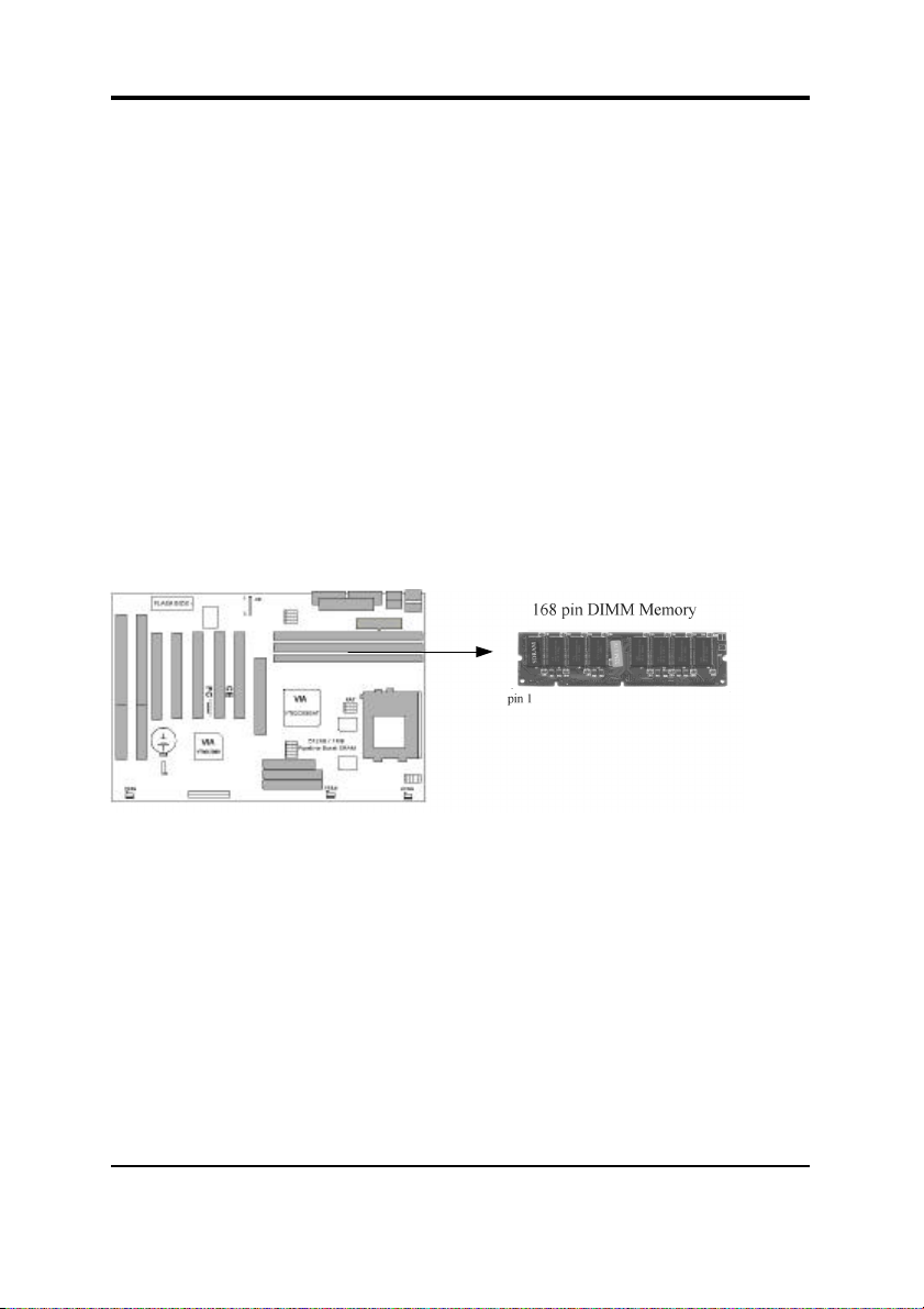
2.3 Installation of Memory
S7-MVP3 motherboard has 3x168-pin 64-bit Dual Inline Memory
Module(DIMM)sockets divided into 3 banks. You can install 3.3V Extended
Data Output(EDO)or Unbuffered Synchronous DRAM(SDRAM)memory. This
will increase the system reliability.
2.3.1 Installation of 168-pin DIMM
1. Before inserting the DIMM, make sure the pin1 of the DIMM matches with
the pin1 on the DIMM socket.
2. Insert DIMM into the DIMM sockets at a 90-degree angle and press down.
2.3.2 Removal of 168-pin DIMM
1. Press the holding clips on both sides of the socket outward to release the
DIMM.

15
2. Gently pull the DIMM out of the socket.
2.3.3 Memory Configuration
There is no jumper setting required for the memory size or type. It is
automatically detected by the system BIOS, and the total memory size is to add
them together.
DIMM Socket DIMM Modules
DIMM1 EDO/SDRAM 8, 16, 32, 64, 128MB
DIMM2 EDO/SDRAM 8, 16, 32, 64, 128MB
DIMM3 EDO/SDRAM 8, 16, 32, 64, 128MB
The S7-MVP3 Motherboard has been tested with the memory listed below.
Size/Type Vendor Model Side Chip
Count SPD
16MB/SDRAM Fujitsu 811171622A-100FN x2 8 No
16MB/SDRAM Hitachi HM5216805TT10 x1 8 No
16MB/SDRAM HY57V168010BTC-10 X1 8Yes
32MB/SDRAM Mitsubishi M5M4V16S30BTP-10 x2 16 No
32MB/SDRAM Mitsubishi M5M4V16S30BTP-10 x2 16 Yes
32MB/SDRAM OKI M56V16800D-10 X2 16 No
32MB/SDRAM HY57V168010BTC-10 x2 16 Yes
32MB/SDRAM TI TMS626812DGE-12A x2 16 No
32MB/SDRAM Micronic MT48LC2M8A1-12 x2 16 No
64MB/EDO Panasonic MN41V17400CTT-06 X2 32 No
128MB/SDRAM NEC D4564841G5-A10-9JF x2 16 No

16
2.4 I/O Connections/Panel Connections
I/O Connections
CN1 ATX Power Connector
JIR1, IR IrDA Connector ( Cable optional )
FDD1 Floppy Disk Drive Connector
IDE1, 2 Primary/ Secondary IDE Connectors
PS2, J2 PS/2 Mouse Port
KB, J1 Keyboard Connector
COM1,2 Serial Ports 1 & 2
LPT1 Printer Port
JUSB1 USB Connector
2.4.1 ATX Power Connector (20-pin CN1)
Make sure that the power supply is off before connecting or disconnecting the
power cable.
2.4.1 Power, Chassis & CPU Fan Connectors (3-pin FAN)
Connect the fan’s plug to the board taking into consideration the polarity of the
connector.

17
2.4.2 IrDA Connector (5-pin JIR1 & IR)
This connector supports the optional wireless transmitting and receiving
infrared module, with this module and application software such as Laplink or
Win95 Direct Cable Connection, user can transfer files to or from their laptops,
notebooks, PDA, PCs and printers. The connector supports HPSIR (115.2Kbps,
2 meters) . Install infrared module onto IrDA connector and configure the
setting through ‘UART 2 Mode’in Integrated Peripherals to select.
whether UART is directed for use with COM2 or IrDA.

18
2.4.2 Floppy Disk Drive Connector (34-pin FDD1)
This connector supports the provided floppy disk drive ribbon cable. Orient the
red stripe to pin 1
2.4.5 Primary/Secondary IDE Connector (Two 40-pin IDE)
These connectors support the provided IDE hard disk ribbon cable. Connect
your first IDE hard disk to master mode of the primary channel. If you have
second IDE device to install in your system, connect it as slave mode on the
same channel, and the third and fourth device can be connected on secondary
channel as master and slave mode respectively.
2.4.6 PS/2 Mouse Port (6-pin Mini-Din PS2 & 4-pin J2)
The system will direct IRQ12 to the PS/2 mouse.

19
2.4.7 Keyboard Connector (6-pin Mini-Din KB & 4-pin J1)
This connection is for a standard keyboard using a PS/2 plug. You may use a
Din to Mini-Din adapter on standard AT keyboards.
2.4.7 Serial Port (Two 9-pin D-type COM)

20
2.4.8 Printer Port (25-pin D-type LPT1)
You can enable the parallel port and choose the IRQ through the “Onboard
Parallel Port”setting in Integrated Peripherals of the COMS SETUP
UTILITY.
2.4.9 USB Connectors (Two 4-pin USB)
You can attach USB devices to the USB connector.
This manual suits for next models
1
Table of contents


