VORAGO PEB1 User manual

PEB1 USER MANUAL
Evaluation board for VA416x0 MCU from VORAGO
JUNE 20, 2020
VORAGO TECHNOLOGIES

VA41620/VA41630 Evaluation Board User’s Manual
V1.0
1
Contents
1 Introduction ........................................................................................................................... 2
1.1 Purpose of Document .................................................................................................... 2
1.2 Overview of Hardware and Software components ........................................................ 2
1.3 Key components included on the PEB1 evaluation kit (subject to change depending on
availability). ................................................................................................................................ 2
1.4 PEB1 MCU board component placement diagram ........................................................ 5
1.5 Connector pin assignment table for MCU board ........................................................... 6
1.6 Materials List .................................................................................................................. 7
1.7 Board connectivity ......................................................................................................... 7
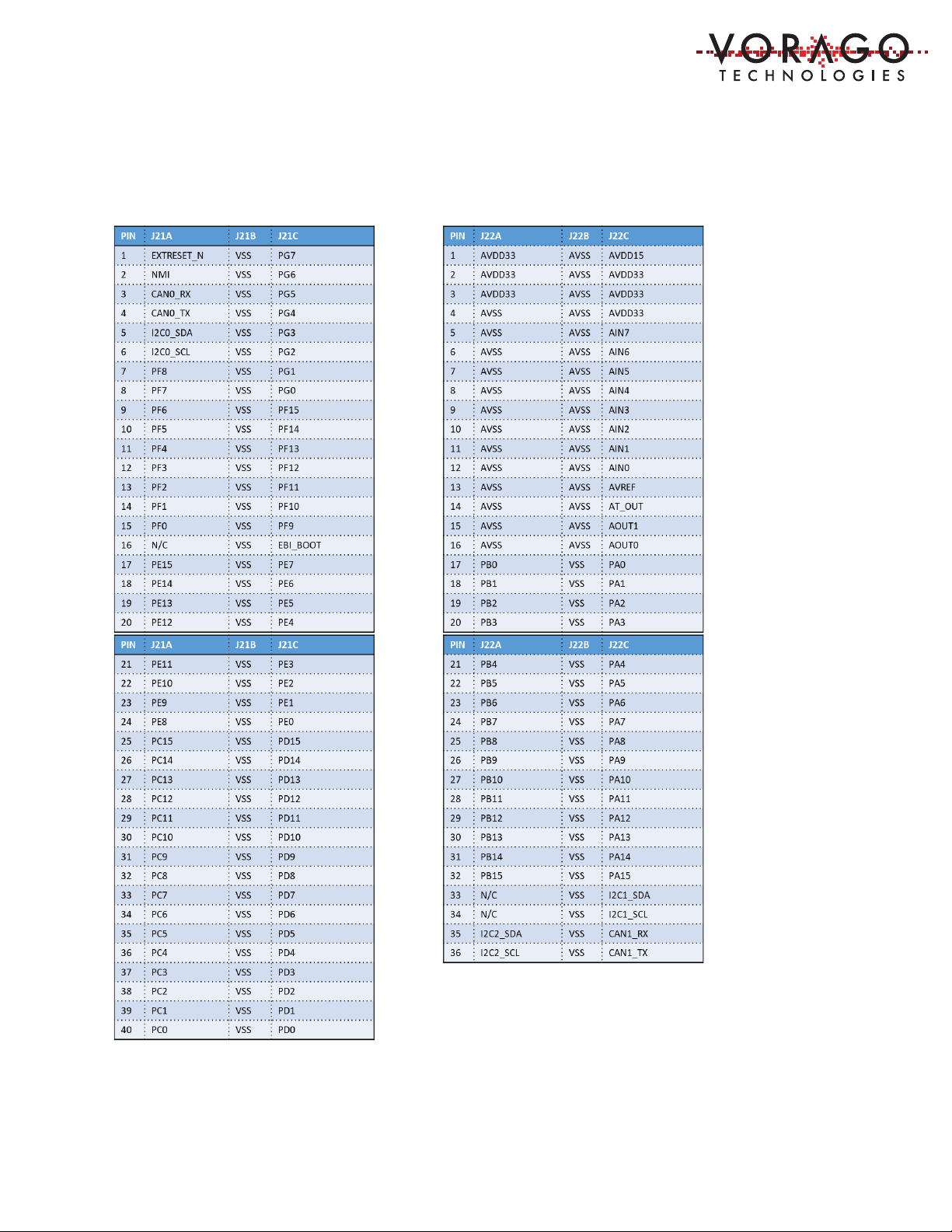
1.8 Connector pin assignment table for GPIO board ........................................................... 8
1.9 Support ......................................................................................................................... 13
2 Software Setup ..................................................................................................................... 13
2.1 Required Downloads .................................................................................................... 14
3 Hardware check ................................................................................................................... 17
3.1 Powering up the board ................................................................................................. 17
4 Command line control of the EVK ........................................................................................ 17
4.1 J-Link OB and RTT (Real Time Terminal) ....................................................................... 20
5 Starting an IDE and building a program ............................................................................... 23
5.1 Keil IDE – ....................................................................................................................... 23
5.2 Programming procedure (Keil Specific) ........................................................................ 31
6 Software Development Kit ................................................................................................... 33
6.1 Project organization ..................................................................................................... 33
6.2 CMSIS compatible driver .............................................................................................. 34
6.3 Preprocessor directives ................................................................................................ 34
7 Commonly asked questions ................................................................................................. 35
8 Other resources for VA416x0 code ...................................................................................... 36
9 Revision history .................................................................................................................... 36

VA41620/VA41630 Evaluation Board User’s Manual
V1.0
2
1 Introduction
1.1 Purpose of Document
This document provides instructions on how to use the features of the VORAGO PEB1
evaluation kit (EVK) and provides a working platform for software development for either the
VA41620 or VA41630 MCUs from VORAGO. The VA41630 has an integrated, internal 2Mb NVM
memory device that contains the user’s program loaded into the MCU at boot. In all other
ways, the VA41620 and VA41630 MCU devices are identical.
1.2 Overview of Hardware and Software components
The PEB1 evaluation kit comprises three printed circuit boards.
• The PEB1 MCU board (top board)
• The PEB1 GPIO board
• The PEB1 EBI/Ethernet board
1.3 Key components included on the PEB1 evaluation kit (subject to change depending
on availability).
• The PEB1 MCU board
o VORAGO VA416x0 MCU
o IDT 501MLFT PLL clock multiplier
o Cypress FM25V20A FRAM
o ST Micro STM32F103C4 MCU0
o Three voltage regulators
• The PEB1 GPIO board
o Two TI isolated CAN transceivers
o Cypress FM25V20A FRAM
o ST Micro LIS2DE12TR accelerometer
• The PEB1 EBI/Ethernet board
o Two TI isolated CAN transceivers
o Microchip KSZ8041TL Ethernet PHY
o Cypress CY7C1041GE SRAM
o Cypress FM22L16 FRAM
1.3.1 The PEB1 MCU board
The PEB1 MCU board includes a SEGGER JTAG Probe, the J-Link OB interface. A separate JTAG
debug pod is not required however a dedicated connector is provided if a different tool is
preferred. SEGGER Microcontroller is VORAGO’S preferred supplier of hardware and software

VA41620/VA41630 Evaluation Board User’s Manual
V1.0
3
development tools. The J-Link OB allows the board to be connected directly to the USB port of
a PC to allow:
- Power supplied from the USB 5V source supply
- JTAG communications for debug and programming
- Terminal communications to allow data transfer between a PC terminal window and
the VA416x0 MCU.
A block diagram of the MCU evaluation board is shown in Figure 1. The MCU evaluation board
conveniently stacks on to resource boards for maximum development flexibility. If compact size
is preferred, the MCU board may be used standalone with full JTAG and includes a UART for
background communication.
Figure 1 - Block diagram of PEB1
1.3.2 The PEB1 GPIO board
The PEB1 GPIO board provides additional connectivity to the VA416x0 MCU. Access to all 104
GPIO pins are available on the various convenient headers. Header pins located on the GPIO
board as well provide access to integrated board resources, ADC inputs, DAC outputs, I2C
interfaces, CAN interfaces with transceivers, and a connector for a SpaceWire interface. An
accelerometer is provided on the board as well, with access via one of the three I2C interfaces.
An external SPI accessible FRAM device is also included on the board. Four PMOD connectors
are available for the I2C, UART, and SPI peripherals.

VA41620/VA41630 Evaluation Board User’s Manual
V1.0
4
Figure 2 - Block diagram of PEB1 GPIO board
1.3.3 The PEB1 EBI/Ethernet board
The PEB1 EBI/Ethernet board provides additional connectivity to the VA416x0 MCU. To suit
another example of port expansion, covering a different set of peripherals, the External Bus
Interface (EBI)/Ethernet interface board provides access to 41 GPIO pins as well as access to
ADC inputs, DAC outputs, I2C interfaces, CAN interfaces with transceivers, and a connector to
the SpaceWire interface. Two high speed parallel memory devices, an SRAM and a FRAM are
included. The VA416x0 Ethernet peripheral is connected to an external Ethernet physical layer
transceiver device and an RJ-45 connector.
Figure 3 - Block diagram of PEB1 EBI-Ethernet board

VA41620/VA41630 Evaluation Board User’s Manual
V1.0
5
1.4 PEB1 MCU board component placement diagram

VA41620/VA41630 Evaluation Board User’s Manual
V1.0
6
Figure 2 - Photo of PEB1 MCU board with functional circuits identified
1.5 Connector pin assignment table for MCU board
The schematics for the three boards are included in PEB1 download package. To assist with
quickly finding which pins are tied to the various connectors on the board, the following set of
tables are provided.
Table 1 - PEB1 MCU Board Connector designations
The PLL clock source provided on the MCU board is clocked with a 20MHz crystal oscillator. The
default setting on the board will provide a 40MHz clock input to the MCU. JP8 pins 7 and 8 are

VA41620/VA41630 Evaluation Board User’s Manual
V1.0
7
tied together. Additional jumpers placed on JP8 can configure a different clock frequency for
the MCU as follows.
Table 2 - PEB1 MCU Board Connector designations for clock selection
1.6 Materials List
• PEB1 evaluation boards – Programmed with demonstration program
• 36” Micro USB cable
• Insert card with component placement picture and URL
• 10 jumpers and several wires
1.7 Board connectivity
This photo shows the PEB1 MCU board mounted onto the PEB1 GPIO board. The connection
between these two boards is made by aligning the plastic pins on the lower board with the
holes on the upper board. Similar connectivity is achieved with the PEB1 MCU board and the
PEB1 EBI/Ethernet board.

VA41620/VA41630 Evaluation Board User’s Manual
V1.0
8
1.8 Connector pin assignment table for GPIO board
The GPIO board has two large 0.1in headers, labeled J21 and J22. The connections to the MCU
are as follows.

VA41620/VA41630 Evaluation Board User’s Manual
V1.0
9
Table 3 - PEB1 GPIO Board Connector designations

VA41620/VA41630 Evaluation Board User’s Manual
V1.0
10
Table 4 - PEB1 GPIO Board Connector designations
PEB1 EBI/Ethernet board (shown without the PEB1 MCU board attached). The connection
between the two boards is made by aligning the plastic pins on the lower board with the holes
on the upper board.

VA41620/VA41630 Evaluation Board User’s Manual
V1.0
11

VA41620/VA41630 Evaluation Board User’s Manual
V1.0
12
Table 5 - PEB1 EBI/Ethernet Board Connector designations

VA41620/VA41630 Evaluation Board User’s Manual
V1.0
13
Table 6 - PEB1 EBI/Ethernet Board Connector designations
1.9 Support
2 Software Setup
Three sets of software will be working in concert:
- Integrated Development Environment (IDE) {Either Keil, IAR or iSystem},
- Segger J-Link RTT viewer and
- Embedded code running on the VA416x0 processor.
The IDE allows code to be developed, compiled, debugged and programmed to an SPI FRAM on
the MCU board. The J-Link RTT Viewer allows terminal communication between the PC and the
VA416x0 MCU. Keys pressed on the keyboard can be routed to the VA416x0 MCU and printf
statements from the VA416x0 MCU can either be logged into a file or shown on a terminal
window. See Figure 3 - Software interaction for PEB1.

VA41620/VA41630 Evaluation Board User’s Manual
V1.0
14
Figure 3 - Software interaction for PEB1
2.1 Required Downloads
The following downloads are required to allow full functionality of the evaluation board. These
tools are evaluation versions and are free of charge. Please download the Keil IDE, the Segger J-
Link software and the VORAGO PEB1 software development code as outlined in the below
sections.
2.1.1 Keil Vision Integrated Development Environment
Keil offers an evaluation version of the IDE for free that will support compiled code of 32kbytes
and below. http://www.keil.com/arm/mdk.asp (approximately size = 400 Mbytes)

VA41620/VA41630 Evaluation Board User’s Manual
V1.0
15
Please use the default directories for the “core” and “pack” when prompted for information
during the install.

VA41620/VA41630 Evaluation Board User’s Manual
V1.0
16
Before the MDK install is complete, the pack installer dialogue will open. Let it run to
completion and then close it. The VA416xx.pack will be loaded later when we open the project.
2.1.2 Segger J-Link
https://www.segger.com/jlink-software.html
Select Software and documentation pack for Windows V6.10n [23,162 KB]. If a later
version is available, please use it.
2.1.3 VORAGO Software and Documentation
http://voragotech.com/PEB1.
This will have the following components in a single .zip file:

VA41620/VA41630 Evaluation Board User’s Manual
V1.0
17
• VA416x0 Software Development kit (Folder structure with many *.c, *.h and
Project files)
• VA416x0 Software Documentation (html file structure)
• VA416x0 Pack file with programming algorithms, header and .SVD files. (Single
.zip file that can either be open separately or by the Keil IDE)
• PEB1 Schematic (Three .pdf documents)
o PEB1 MCU board
o PEB1 GPIO board
o PEB1 EBI/Ethernet board
• PEB1 User’s Manual (Single .pdf document)
• PEB1 Quick Start Guide (Single .pdf document)
3 Hardware check
3.1 Powering up the board
The Segger J-Link driver needs to be loaded prior to plugging the board to a PC. See 2.1.2.
• Before connecting the board conduct a jumper check. Only the following jumpers
should be inserted:
o 5v supply from USB jumper on JP10
o Clock source JP8. Jumper between pins 7 and 8.
o MCU voltage 3.3v and 1.5v supply shunts on JP4 (pin 5 to 6 and pin 7 to 8)
o Analog voltage supply connections on JP15 (all four jumpers in place)
• Connect the USB cable between PC and the PEB1 board
o The green DS1 LED will indicate that power is applied to the board.
• If the MCU has the pre-programmed example code running, the green LED DS2 will blink
to show that the code is running.
o Pressing the RESET button (SW1) will hold the device in RESET. Releasing it will
commence the boot sequence and start code executing.
4 Command line control of the EVK
By using “PuTTY” or “Tera Term”, terminal window interface applications, it is possible enter
commands and monitor the outputs in a log file or terminal window.
The following table contains all the supported commands that the firmware will recognize.

VA41620/VA41630 Evaluation Board User’s Manual
V1.0
18
Command
Arguments
Comments
$help
none
Provides list of all available commands
$help
$readport [port 0-6] [mask] – Masked pins input, read IO port
$setport [port 0-6] [mask] [val] - Set masked pins hi/loon Port output 1 or 0
$readadc [ch 0-15] - Readan ADC channel
$setdac [0 or 1] [0x0 – 0xfff] – Set DAC0 or DAC1 output
$romlwr [addr] [data32] – Write word to SPI boot FRAM
$romlrd [addr] Read word from SPI boot FRAM
$auxwr [addr] [data32] - Write word to aux FRAM
$auxrd [addr] – Read word from aux FRAM
$ebiinit – Initialize external mem interface
$ebiwrite [addr] [data32] – Write word to EBI
$ebiread [addr] – Red word from EBI
$cantest – CAN bus loopback test
$ethtest – Ethernet test
$spwtest – SpaceWire test
$i2ctest – I2C test I2C1(m) -. I2C2(s)
$accel [(opt) 1: enable every sec] – Get accelerometer data
$brdtmp [(opt) 1: en every sec] – Get board temperature
$rsts – Read reset source register
$fwver – Get firmware version
$srst – Software reset
$help – Print help
Note:
$i2ctest - Requires I2CA and I2CB be externally connected together
$cantest – Requires CAN0 and CAN1 be externally connected together
$readport
[portNum] [mask]
Ports A through port G are read and a 16-bit hex value is displayed for ports A-F and 8-bit hex
value is read for port G. Ports A through G are accessed with portNum 0 through 6.
Example: $readport 0 0x00ff
Response: OK 0x1234
Note: Some GPIO are dedicated to certain peripherals by the software included with this
package.
PORTA [7:4]: SPI2
PORTB [15:12]: UART1
PORTF [5:2]: SPI1
PORTF [9:6]: UART2
PORTG [1:0]: UART0
PORTG [4]: SPI1 (FRAM chip select)
$setport
[portNum] [mask]
[val]
Sets a single port to a value depending on the mask
Example: $setport 0 0x00ff 0x0055
Response: “OK if port number is valid, “ERR is reported for invalid port number.
$readadc
[channelNum]
Reads the value of the specified ADC channel
Example: $readadc 11
Response: $OK 0x0373
$setdac
[dacNum] [data]
Sets the output of DAC0 or DAC1 to the voltage corresponding to the data [hex value 0x0 to
0xfff]
Example: $setdac 0 0x800
Response: $OK
ANOUT0 will be set to ½ VDDREF, or about 1.65v
$rom1wr
[addr] [data32]
Writes one address location of the SPI boot FRAM device.
Example: $rom1wr 0x0 0x0

VA41620/VA41630 Evaluation Board User’s Manual
V1.0
19
Response: $OK
$rom1rd
[addr]
Reads one address location from the SPI boot the FRAM device.
Example: $rom1rd 0x0
Response: $OK 0x00000000
$auxwr
[addr] [data32]
Writes one address location of the external FRAM device.
Example: $auxwr 0x0 0x0
Response: $OK
$auxrd
[addr]
Reads one address location from external the FRAM device.
Example: $auxrd 0
Response: $OK 0x00000000
$ebiinit
None
Initializes the external memory interface.
Example: $ebiinit
Response: $OK
$ebiwrite
[addr] [data32]
Writes one address location of the memory device connected to the EBI.
Example: $ebiwrite 0x60000000 0x0
Response: $OK
$ebiread
[addr]
Reads one address location of the memory connected to the EBI.
Example: $ebiread 0x60000000
Response: $OK 0x00000000
$cantest
None
Performs a test of both CAN interfaces.
Example: $cantest
Response: $OK
$ethtest
None
Performs a test of the Ethernet interface.
Example: $ethtest
Response: $ERROR cmd status: notImplemented
$spwtest
None
Performs a test of the SpaceWire interface
Example: $spwtest
Response: $ERROR cmd status: notImplemented
$i2ctest
None
I2C test of I2C1 and I2C2. This assumes the SCL and SDA lines are connected together.
Example: $i2ctest
Response: ‘$OK:
$ERROR nack’ if no response
Will hang up if the top board is not connected to the bottom board
Device will lose its connection to the J-Link RTT terminal and will have to be reconnected.
Table of contents
Other VORAGO Motherboard manuals