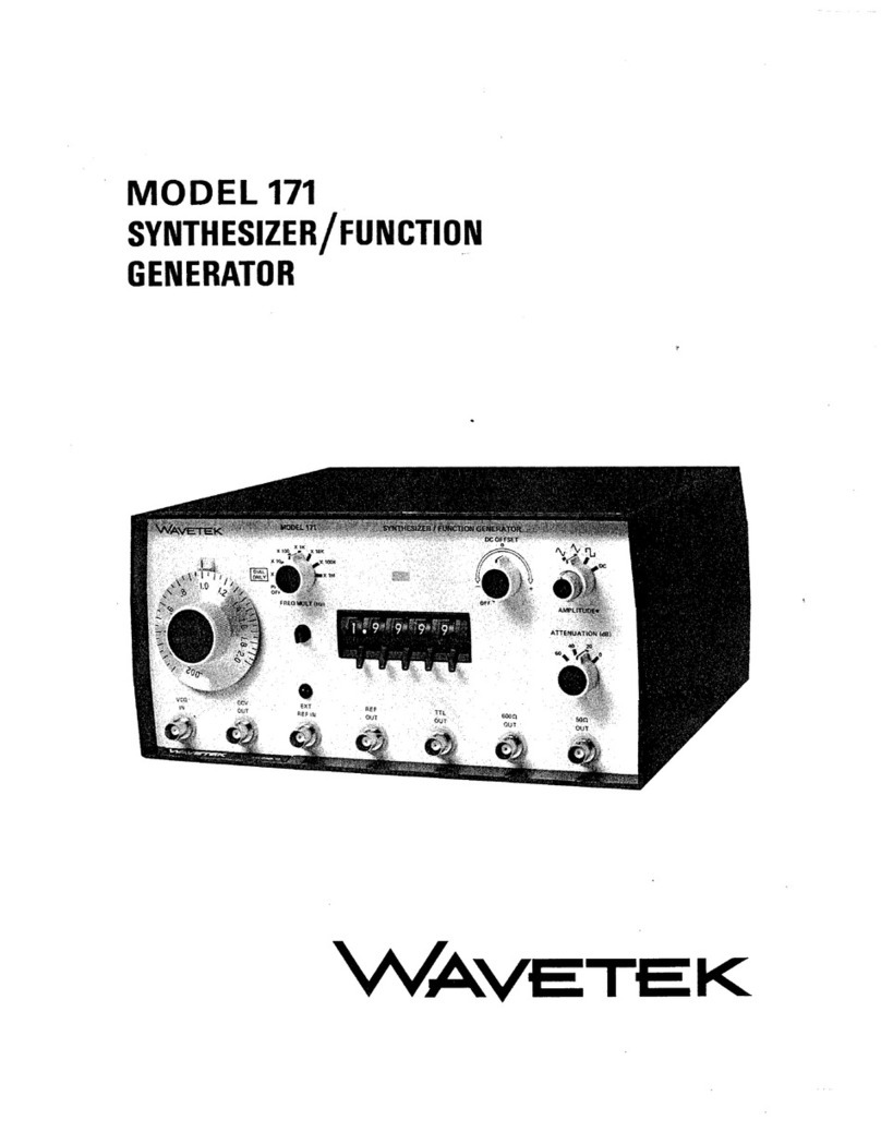
Wavetek 5100 User manual

INSTRUCTION
MANUAL
MODELS 5100 AND 5110
0.001
HZ-2
MHz
PROGRAMMABLE FREQUENCY
SYNTHESIZERS
O
1981
Wavetek
THIS DOCUMENT CONTAINS INFORMATION PRO-
PRIETARYTO WAVETEK AND IS PROVIDEDSOLELY FOR
INSTRUMENT OPERATION AND MAINTENANCE. THE
INFORMATION IN THIS DOCUMENT MAY NOT
BE
DUPLICATED IN ANY MANNER WITHOUT THE PRIOR
APPROVAL IN WRITING FROM WAVETEK.
WAVETEK SAN DIEGO, INC.
9045 Balboa Ave., San Diego, CA 92123
P.
0.
Box 85265, San Diego, CA 92138 Manual Revision: 4188
Tel
61
91279-2200
TWX
9101335-2007 Manual Part
Number:
00-800-1
51
0
*

DIGITALY REMASTERED
OUT OF PRINT- MANUAL SCANS
By
Artek Media
18265 200th St.
Welch, MN 55089
www.artekmedia.com
“High resolution scans of obsolete technical manuals”
If your looking for a quality scanned technical manual in PDF format please visit
our WEB site at www.artekmedia.com or drop us an email at
manuals we have available.
If you don’t see the manual you need on the list drop us a line anyway we may
still be able to point you to other sources. If you have an existing manual you
would like scanned please write for details. This can often be done very
reasonably in consideration for adding your manual to our library.
Typically the scans in our manuals are done as follows;
1) Typed text pages are typically scanned in black and white at 300 dpi.
2) Photo pages are typically scanned in gray scale mode at 600 dpi
3) Schematic diagram pages are typically scanned in black and white at 600
dpi unless the original manual had colored high lighting (as is the case for
some 70’s vintage Tektronix manuals).
4) Most manuals are text searchable
5) All manuals are fully bookmarked
All data is guaranteed for life (yours or mine … which ever is shorter). If for ANY
REASON your file becomes corrupted, deleted or lost, Artek Media will replace
the file for the price of shipping, or free via FTP download.
Thanks
Dave & Lynn Henderson
Artek Media

WARRANTY
Wavetek warrants that all products manufactured by Wavetek conform to published
Wavetek specifications and are free fromdefects in materialsandworkmanship for a period
of one
(1)
year from the date of delivery when used under normal operating conditions
and within the service conditions for which they were furnished.
The obligation of Wavetek arising from a Warranty claim shall be limited to repairing, or
at its option, replacingwithout charge, any product which in Wavetek's sole opinion proves
to bedefective within the scope of the Warranty. Inthe event Wavetek is not able to modify,
repair or replace non-conforming defective parts or components to a condition as
warrantied within a reasonable time after receipt thereof, Buyers shall becreditedfor their
value at the original purchase price.
Wavetek must be notified in writing of the defect or nonconformity within the Warranty
period andthe affectedproduct returnedto Wavetek's factory or to an authorized service
center within
(30)
days after discovery of such defect or nonconformity.
For product warranties requiring returnto Wavetek, productsmust be returnedto a service
facility designated by Wavetek. Buyer shall prepay shipping charges, taxes, duties and
insurance for products returned to Wavetek for warranty service. Except for products
returned to Buyer from another country, Wavetek shall payfor returnof productsto Buyer.
Wavetek shall have no responsibility hereunder for any defect or damage caused by
improper storage, improper installation, unauthorized modification, misuse, neglect,
inadequate maintenance,accident or for any product which has been repaired or altered
by anyone other than Wavetek or itsauthorized representative and not inaccordancewith
instructions furnished by Wavetek.
Exclusion of Other Warranties
The Warranty described above is Buyer's sole and exclusive remedy and no other
warranty, whether written or oral, is expressed or implied. Wavetek specifically
disclaims the impliedwarranties of merchantability andfitness for a particularpur-
pose. Nostatement, representation, agreement, or understanding, oral or written, made
by an agent, distributor, representative, or employee of Wavetek, which is not contained
in the foregoing Warranty will be binding upon Wavetek, unless made in writing and
executed by an authorized Wavetek employee. Under nocircumstancesshallWavetek
be liable for any direct, indirect, special, incidental, or consequential damages,
expenses, lossesordelays (includinglossof profits)based oncontract, tort, orany
other legal theory.

SECTION
1
GENERAL DESCRIPTION
.
.....................................
1 1 MODELS 5100 and 5110 1-1
1.2 SPECIFICATIONS
..........................................
1-1
1.2.1 Frequency
...............................................
1-1
1.2.2 Frequency References
.....................................
1-1
.........................................
1.2.3 Output Amplitudes 1-1
1.2.4 Output Level Control
.......................................
1-2
1.2.5 Spectral Purity
..........................................
1-2
.........................
1.2.6 Remote Mode Selection (Model 5100) 1-2
1.2.7 Switching Charactoristics
...................................
1-2
....................................................
1.2.8 GPlB 1-2
1.2.9 General
..................................................
1-2
1.2.10 Options
.................................................
1-2
.............................................
1.2.11 Accessories 1-2
SECTION
2
INSTALLATION
2.1 INSPECTION
............................................
2-1
2.2 POWER REQUIREMENTS
.....................................
2-1
2.3 INSTALLATION
............................................
2-1
2.3.1 Model 5100
...............................................
2-2
...............................................
2.3.2 Model5110 2-2
.....................
2.4 INITIAL CONFORMANCE TEST PROCEDURE 2-2
SECTION
3
OPERATION
.
3.1 INTRODUCTION
............................................
3-1
3.2 POWER SWITCH AND INDICATOR
.............................
3-1
...........................................
3.3 SYSTEM CLOCKS 3-1
...................
3.3.1 Internal Reference
(8
MHz Crystal Oscillator) 3-1
...........................
3.3.2 External Reference (REF IN Signal) 3-1
..................
3.3.3 Phase-Locking to an External 1 MHz Standard 3-1
.......................
3.3.4 Phase-Locking Two or More Instruments 3-3
..........................................
3.4 OUTPUT SIGNALS 3-3
3.4.1 Model 5100 Main Outputs
...................................
3-3
3.4.2 Model 5110 Main Outputs
...................................
3-3
3.4.3 Models 5100 and 5110 Reference Output Signals
...............
3-3
3.5 REMOTE SWITCH AND INDICATOR (Model 5100 Only)
............
3-3
3.6 LOCAL MODE OPERATION (Model 5100 Only)
....................
3-3
3.6.1 Local Frequency Control
....................................
3-4
3.6.2 Local Attenuation and Level Control
...........................
3-4
3.7 REMOTE MODE OPERATION (Models 5100 and 5110)
.............
3-5
........................................
3.7.1 Programming Lines
3-5
...............
3.7.2 Remote-Local Mode Transitions (Model 5100 Only) 3-9
SECTION
4
CIRCUIT DESCRIPTION
.....................................
4.1 SlNUSOlD GENERATION 4-1
................................
4.2 FUNCTIONALBLOCKTHEORY 4-1
4.3 PROGRAMMING
............................................
4-1
iii

CONTENTS
(Continued)
SECTION
5
OPTIONS
....
......
........................
5.1 GENERAL
..
....
5-1
5.2 OPTION 001. HIGH STABILITY REFERENCE OSCILLATOR
.........
5-1
5.3 OPTION 002. REMOTE ATTENUATION
.........................
5-1
5.4 OPTION 004, 10 VOLT P-P OUTPUT (Model 5110 Only)
..........
5-1
5.5 OPTION 006, TEMPERATURE COMPENSATED
......
...............................
CRYSTAL OSClLLATOR 5-1
5.6 OPTION 013, UPPER FREQUENCY RANGE EXTENSION
..........
5-1
5.7 OPTION 020. TTL OUTPUT
................................
5-1
SECTION
6
CONFORMANCE TESTS
6.1 INTRODUCTION
...........................................
6-1
6.2 POWER SUPPLY
...........................................
6-1
6.3 CLOCKGENERATOR
.......................................
6-2
6.4 FRONT PANEL DATA (Model 5100 Only)
.......................
6-2
6.5 SAMPLEGENERATOR
.....................................
6-2
6.6
DC
OFFSET
..............................................
6-2
6.7 FRONT PANEL FREQUENCY (Model 5100 Only)
................
6-5
6.8 REMOTE MODE
................................
..
.......
6-6
6.9 INTERNAL OSCILLATOR
..................................
6-6
6.1
0
STANDARD ATTENUATOR (Model 5100 Only)
..................
6-7
6.11 PROGRAMMABLEATTENUATOR (Option 002 Units Only)
.........
6-7
SECTION
7
TROUBLESHOOTING
7.1 INTRODUCTION
..........................................
7-1
...................
7.2 TROUBLESHOOTING CHART INSTRUCTIONS 7-1
.............
7.3
PART DESIGNATION AND IC SOCKET NUMBERING 7-1
SECTION
8
STANDARD CIRCUITRY PARTS AND SCHEMATICS
8.1 DRAWINGS
.........................................
8-1
8.2 ORDERING PARTS
.........................................
8-1
8.3 ERRATA
.................................................
8-1
APPENDIX A OPTION 013. 3
MHz
FREQUENCY RANGE
A.l GENERAL
................................................
A-I
A.2 OPERATION
..............................................
A-I
APPENDIX B OPTION 020. TTL OUTPUT
................................................
B.l GENERAL B-1
B.2 OPERATION AND CIRCUIT DESCRIPTION
......................
B-1

LlST OF ILLUSTRATIONS
Installing Rack Mount Bracket on Model 5100
...............................
2-1
Instrument Front and Rear Panels
........................................
3-2
.............................................
Attenuator Response Curves 3-4
..........................................
Standard Program Line Circuitry 3-5
Rear Panel Programming Connector
.......................................
3-6
Zero Phase Line Circuitry
...............................................
3-6
Remote.Programming Chart
.............................................
3-8
Loading Timing Diagram
................................................
3-10
Direct Digital Synthesis
.................................................
4-1
Sine Wave Generation
..................................................
4-2
Motherboard Assembly A1
...............................................
6-3
Waveform at Point DC
..................................................
6-4
Waveform for FPD
.....................................................
6-4
Sample Waveform Generator
............................................
6-5
DIP Pin Numbering
.....................................................
7-2
...................................................
Basic Timing Signals 7-5
Accumulator Signals
....................................................
7-8
LlST OF TABLES
7-1 Troubleshooting Chart
..................................................
7-2
A-1 Output Signal Characteristics (Option 013)
.................................
A-1

DRAWINGS
DRAWING
TITLE
SECTION
5
Option 001 Assembly and Parts List
Option 002 Remote Attenuator Schematic
Option 002 Remote Attenuator Assembly
Option 002 Remote Attenuator Parts List
Options 004 and 006 Parts Lists
SECTION
8
Final Assembly
Final Assembly Parts List
Chassis Assembly
Chassis Parts List
Mainboard Schematic
Mainboard Assembly
Mainboard Assembly Parts List
Attenuator Schematic (Local)
Attenuator Assembly and Parts List (Local)
Front Panel Assembly
Front Panel Parts List
Final Assembly
Final Assembly Parts List
Chassis Assembly
Chassis Parts List
Mainboard Schematic
Mainboard Assembly
Mainboard Assembly Parts List
Front Panel Parts List
Scanner Schematic
Scanner Assembly and Parts List
10 Bit DA Converter Schematic
10 Bit DA Converter Assembly
10 Bit DA Converter Parts List
Regulator Assembly and Parts List

TITLE
DRAWING
Rear Panel Assembly
Rear Panel Parts List
Bottom Cover Assembly and Parts List
Side Frame Assembly and Parts List
APPENDIX A
Option 013 Final Assembly
Option 013 Final Assembly Parts List
Option 013 Chassis Assembly
Option 013 Chassis Parts List
Option 013 Mainboard Schematic
Option 013 Mainboard Assembly
Option 013 Mainboard Parts List
Front Panel Assembly
Front Panel Parts List
Option 013 Final Assembly
Option 013 Final Assembly Parts List
Option 013 Chassis Assembly
Option 013 Chassis Parts List
Option 013 Mainboard Schematic
Option 013 Mainboard Assembly
Option 013 Mainboard Parts List
APPENDIX
B
Option 020 Final Assembly and Parts List
Option 020 Schematic, Assembly and Parts List

SAFETY FIRST
Protect yourself.
Follow these precautions:
Don'ttouchthe outputsof the instrumentor any exposedtest wiring carryingthe output
signals. This instrument can generate hazardous voltages-andcurrents.
Don't bypass the power cord's ground lead with two-wire extension cords or plug
adaptors.
Don'tdisconnect thegreenandyellowsafety-earth-groundwire that connects the ground
lug of the power receptacle to the chassis ground terminal (marked with @or&.
Don't hold your eyes extremely close to an rf output for a long time. The normally
nonhazardous low-power rf energy generated by the instrument couldpossibly cause
eye injury.
Don't plug in the power cord until directed to by the installation instructions.
Don't repair the instrumentunlessyou are
a
qualifiedelectronicstechnicianand know
how to work with hazardous voltages.
Payattentiontothe
WARNING
statements.Theypointoutsituationsthat cancauseinjury
or death.
PayattentiontotheCAUTIONstatements.Theypointoutsituationsthat cancauseequip-
ment damage.
viii

GENERAL DESCRIPTION
1.1 MODELS 5100 AND 5110
Models5100 and 5110Programmable Frequency Syn-
thesizers provide spectrally pureoutputfrequencies in
0.001 Hzsteps from DCto
2
MHz. Model5100 may be
programmedlocallyand remotely.Model5110mayonly
be programmed remotely.
A patented* direct digital synthesis technique is used
togenerate theoutputfrequency directlyfrom aninter-
nalcrystal reference,which maybephase lockedtoan
external 1 MHz standard, if desired.
Inaddition to excellent short term stability, digital syn-
thesis also provides other improvements in perf0.t-m-
ance. Digitaloperation means inherent programmabil-
ityandvery fast switching. Inbinarywordformat,these
models maintain
amplitude and phase continuity in
switchingbetween any twofrequencies
(i.e.,noswitch-
ing transient) with a programming delay of only 1.5ps
beforeswitching.Thus,linearfrequencysweepingorfre-
quency hopping (including FSK signaling) are easily
programmed.
Excellent spectral purity is also possible with digital
synthesis sinceoutput distortion isdetermined entirely
by the number of bits per sample and the linearity of
the DIA converter. Another feature of digital synthesis
istheabilitytopreciselycontrolthephaseof the output
frequency.The phase may be asynchronously reset to
zero at any time for as long as desired (or as little as
125ns).Hence,for example,sinusoidalburstsareeasily
produced with each burst beginning at exactly zero
phase.
1.2 SPECIFICATIONS
1.2.1 Frequency
Range
0.001 Hz to 2,000,000.000 Hz.
0.001 Hz to 3,000,000.000 Hz (Option 013).
Resolution
0.001 Hz throughout entire range.
Control
Local (Model 5100 Only):
Ten 10-position rotary
switches.
Remote:
31 bits in binary or 37 bits in BCD format.
*U.S.
Patent
3,735,269
1.2.2 Frequency References
Model 5100
Internal (8 MHz Crystal):
Standard:TCXO(SameasOption006for Model5110).
Option 001
:
High Stability (Oven Controlled).
External, Rear Panel REF
IN
(TTL Level, Schmitt-
Trigger Conditioned Input,
1
TTL Load):
1MHzReference:Phaselockstostandardor optional
internal reference.
8
MHz Reference: Replaces internal
8
MHz crystal
reference.
Model 5110
Internal (8 MHz Crystal):
Option 001
:
High Stability (Oven Controlled).
Option 006: TCXO.
External, Rear Panel REF IN (TTL Level, Schmitt-
Trigger Conditioned Input, 1 TTL Load):
1 MHz Reference: Phase locks to optional internal
reference.
8
MHz Reference: Replaces internal 8 MHz crystal
reference. Required for units without an internal
reference.
1.2.3 Output Amplitudes
Model 5100
FixedOutput:
1Vp-p noload,0.5 Vp-pinto509.Front
panel (1 VOLT
P-P),
rear panel (FXD OUT).
Variable Output:
10Vp-p no load(max),5 Vp-p into
50R (max). Front panel (OUTPUT), rear panel (VAR
OUT).
Model 5110
Fixed Output:
1 Vrms no load, 0.5 Vrms into 50R.
Front panel (OUTPUT 50R), rear panel (FXD OUT).
Option004:
Replaces1Vrms(noload)signalat fixed
output with 10Vp-p signal.
Models 5100 and 5110
Frequency Response(Full Output):
NoLoad:dcto500kHz,
+
0.25dB;500kHzto
2
MHz
(3
MHz with Option 013),
2
0.5 dB.
5052 Load:dcto500kHz,
&
0.25dB;500kHzto2MHz
(3 MHz with Option 013),
+
0.5 to
-
2.5 dB.
Reference Output:
1 MHz square wave or
8
MHz
pulseat
TTL
levels.Capableof driving 30
TTL
loads.
Rear panel (REF OUT).

1.2.4 Output Level Control
Model 5100 only
frequency (phase continuous) and amplitude (with
option 002) as well as all ZERO PHASE modes.
0to85dBattenuationin 1dBsteps(front panelpush-
button)plus0to 10dBfront panelcontinuous control.
Option 002 (Models
51
00 and 5110)
Remoteprogramcontrol(7bits)of 85dBattenuation
in 1
dB
steps from
0
to
85
dB.
Attenuator Responseto 60 dB (Includes Option 002)
To 500 kHz:
+
0.5 dB.
>500 kHz: See figure 3-2.
1.2.5 Spectral Purity
Spurious Components
Standard:
-
70 dB to 100kHz;
-
60 dB to 500 kHz;
-
50 dB to 2 MHz.
Option01
3:
-
45 dB, 500 kHzto 2 MHz;
-
40 dB to
3 MHz.
Harmonic Components (at
1
Vrms)
Standard:
-
55dB to 100kHz;
-
50 dB to 500 kHz;
-
45 dB to 2 MHz.
Option 013:
-
40 dB, 500 kHz to 3MHz.
Phase Noise
30 kHz band excluding 1 Hz centered on carrier.
Standard:
-
50 dB to 2 MHz.
Options 004 or 013:
-
40 dB, 2 MHz to 3 MHz.
RMS Fractional Deviation
10msec averaging:
5
x
10-7,dc to 2 MHz(3 MHz
with Option 013).
1sec averaging:
5
x
10
-
91
dc to2 MHz(3 MHzwith
Option 013).
1.2.6 Remote Mode Selection (Model 51
00)
Via front panelpushbuttonor onecontrolbit. Frontpanel
lamp indicates remote mode.
1.2.7 Switching Characteristics
Programming Delay
1.5~~for BINARY-WORDmodewith phaseandampli-
tude continuity maintained.
20psfor BCD-WORDmodewith output resettozero
phase during delay.
20 ps minimum for four BCD or BINARY bytes with
output reset to zero phase during programming.
Update Rate
625 ns for BINARY-WORD mode. 18 ps for BCD-
WORD and BYTE modes.
Zero Phase Reset
Output signal may be asynchronously reset to zero
phaseviaonecontrolbit.There isadelayof approxi-
mately 800 nsec to the output. This line mayalso be
used as a load acknowledge output.
1.2.8 GPlB
Model1488A-12providesthefollowingIEEE488-1978
functions: AH1, L1 (listen only), DT1. Programs
1.2.9 General
Environment
Operating Temperature:
0" to
+
50°C.
Storage Temperature:
-
20"
to
+
70°C.
Dimensions
43.2 cm (17 in.) wide; 8.9 cm (3% in.) high; 33 cm
(1
3
in.) deep.
Weight
9.6 kg (21 Ib) net; 11.4kg (25 Ib) shipping.
Power
1151230V
+
1O0/o150 to 60 Hz, 65 watts.
1.2.1 0 Options
001:
8
MHz, HighStability Crystal Reference
(Oven Controlled)*
*.
Temperature Stability:
+
1
x
10-8,0" to
+
55°C.
Aging Rate:
+
2
x
10-glday.
002: Remote Programmable Attenuator
Range:
0 to 85 dB in steps of 1 dB.
ProgrammingDelay:
Typically less than 5ms.
004: 10Vp-p Output
Model 5110only. Not available with Option 013.
I
006:
8
MHz, Temperature Compensated Crystal
1
Reference
(
(Standardon Model 5100.)
1
I
Temperature Stability:
&
1
x
10-6,0" to
+
55°C.
Aging Rate:
+.
5
x
10-6/year.
013: Frequency Range Extension
Original order only. Not available with Option 004.
Frequency Range:
0.001 Hz to
3
MHz.
Frequencyresolution:
0.001Hz(RemoteandModel
5100 Local).
Variable Output (Model 5100 Only):
1
Vrms maxi-
mumnoload,0.5Vrmsmaximuminto50R load.50R
source impedance.
Variable Output Signal (Model
5100
Only):
See
table A-1
.
020: Rear Panel
TTL
Output
Providesa
TTL
compatable square wave. Replaces
VAR OUT BNCon Model 5100.See paragraph 1.2.1
for range and resolutionspecifications.
GPlB
Use Model 1488A-12adapter.
1.2.1
1
Accessories
Rack Adapters
Programming ~onnedor
**Specifications apply after a
72
hour warm-up period.

2.1 INSPECTION
2.2
POWER REQUIREMENTS
Thisinstrumentwas carefully inspectedandtestedprior
to shipment. It was operated for at least 100 hours to
reduce the probability of early failure. The instrument
should be inspected for physical damage incurred in
transit. When receiving a shipment from a carrier,
inspecttheshippingcartoninthepresenceof thecarrier.
If roughhandlingisevidenttakeexceptiononthedelivery
receipt before accepting the shipment.
If nocartondamage isobvious,but physicaldamage is
discovered when the carton is opened, preserve the
carton and packing materials, notify the carrier
immediately and have them perform
a
written inspec-
tion of the carton and the contents.
Itis recommendedthat the initialconformance test pro-
cedure be performed on receipt as described in
paragraph
2.4.
This instrument will operate on 115 Vac
(1
10%)
50-60 Hz or 230Vac
(
2
10%)50-60 Hz,selectablevia
a rear panel switch.The instrument is equippedwith a
three-wire power cable which connectsthe chassisto
earthgroundwhen plugged into
a
three-contact outlet.
Ifatwo-contactoutlet isusedinconjunctionwitha
three-
prong andtwo-prong adaptor,the pigtailofthe adapter
should be connected to earth ground.
2.3
INSTALLATION
WARNING
Rack mount brackets are to prevent the
instrumentfromslidingwhen mountedin
a
rack. They are not intended to supportthe
weight of the instrument and should never
be used for lifting or carrying.
RACK
MOUNT'
BRACKET
THESE
EDGES
Figure 2-1. Installing Rack Mount Bracket on Model 5100

2.3.2
Model 5110
2.3.1 Model
51
00
Model
51
00 Frequency Synthesizer was factory
assembledfor benchuse.Toconvertthe instrumentfor
mountingintoa standard 19inchwide rack,the follow-
ingprocedure should befollowed. (Referto figure 2-1
.)
1
.
Unplug instrument from ac power source.
2. Stand instrument on one side.
3.
Align rackmountbracketwith raisededgeof instru-
ment as shown.
4.
Holeson rack mountbracket should correspond to
pemnutholesjust underneathblacktrimstrip. Use
apointedobject topiercethe black trimstrip at the
pem nut holes.
5.
Use lock washers and metal screws provided to
secure rack mount bracket.
6.
Repeat for other side bracket.
Instrument is now ready for rack installation.
Model5110FrequencySynthesizeris readyfor installa-
tion into a standard 19 inch wide rack.
2.4
INITIAL CONFORMANCE TEST PROCEDURE
To verify that the instrument is operational, the follow-
ingprocedureisrecommended. Iftrouble issuspected,
then refertothetroubleshootingsectioninthis manual.
Phase lock the unit and a frequency counter to a com-
monfrequency reference.
A
1
MHz output signal from
the REF OUT connector may be used as a reference
inputto the counter,or a
1
MHzoutput from the counter
.
maybe usedto phaselockthe unit. For details, refer to
paragraph
3.3.3.
ConnecttheOUTPUTjack of the unit tothecounterand
verifythat thecounter istriggered. Programafrequency
of 1
,I11,111-000Hzandverify onthe counter.(A count
of
,+
1 from the true value is acceptable.) Repeatthis
procedure for 1,222,222.000 Hz, etc.

3.1 INTRODUCTION
Figure3-1 shows thefront and rear panelsof the instru-
ment with controls and connectors identified. Model
5100 may be controlled locally with the front panel
switches or remotely via the rear panel programming
connector. Model 5110 is controlled only via the rear
panel programming connector. Frequency is pro-
grammable on all units, while attenuation is pro-
grammable on Option 002 equipped units only.
3.2 POWER SWITCH AND INDICATOR
The front panel POWER switch controls ac line power
to the unit. The green POWER indicator verifies the
presenceof the5Vsupplyfor the digital logic circuitry.
NOTE
For units equipped with'the high-stability
proportional-ovencrystal(Option
001),
power
must
be
maintained
(POWER
indicator on)at
least
72
hoursprior touseif fullaccuracyand
drift performance of the crystal are to be
realized.
3.3 SYSTEM CLOCKS
For the instrument to function, it must have a system
clock derived from either an internal or external
reference. In addition, the internal reference may be
phase-lockedtoanexternal1MHzinputsignal,andtwo
or more instruments may be phase-locked together.
3.3.1 Internal Reference
(8
MHz Crystal Oscillator)
The Model5100containseitherthestandardor optional
(Option001)internal
8
MHzcrystal referenceoscillator.
The standard Model 5110is not supplied with an inter-
nal referenceoscillator, but may contain either Option
001 or 006,
8
MHz reference oscillators.
To enable any internalcrystal reference oscillator, the
lnputReferenceSelectorJumper,locatedinsidetheunit
on the main board(figure 5-1) must be inthe INTposi-
tion.If noexternalsignalisconnectedtotheREF INjack,
the internal crystal frequency may be adjusted as
described in paragraph
6.7
of the Conformance Test
Procedure.
3.3.2 External Reference (REF IN Signal)
Any internal8MHzcrystal reference installedinthe unit
may be either phase-locked to an external
1
MHz
referencesignal,orcompletely replacedbyanexternal
8
MHz signal, which becomes the system clock. An
external 8 MHz reference signal is required for Model
5110 units without an optional internal reference
oscillator. Forexternal
8
MHzreferenceinputoperation,
the INPUT REFERENCE SELECTOR JUMPER located
insidetheunitonthemainboard(drawing002-004-3100)
must be inthe EXT position. The rear panel BNCjack
labeled REF INaccepts either the 1or 8 MHz external
reference input signals.
The absolute maximum voltage limits of the external
reference input signal are
&
5.5 V peak for the Model
5100,and
+
5.0V peakfor the Model 5110. Burden on
the signal source is one standard TTL load. A TTL
Schmitt-trigger circuit conditions the input signal to be
a
hysteresisoutputsignalwith
a
positive-goingthreshold
of
+
2 V maximum and a negative-going threshold of
-
0.6V minimum.The inputsignalwaveform mustcross
both thresholds for 50 ns, minimum, once per cycle.
Ifthe REF IN signal is to bethe system clock,the input
frequency mustbebetweendc and8.1 MHz.Thedevia-
tionof theoutputsignalfrequencyisdirectly proportional
tothedeviationof thesystem clockfrom
8
MHz.Opera-
tionatfrequenciesbelow
8
MHzimpliesalowersampling
rate;theinternallowpassfilterwhich removessampling
components from the output signal is designed for an
8
MHz sampling rate and becomes ineffective as the
samplingrateislowered.To maintainfull harmonic and
spuriousdistortion specifications,anexternallow pass
filter is required to eliminate these components.
3.3.3 Phase-Lockingto an External 1 MHz Standard
For phase-locking to an external standard, the instru-
ment must be equipped with an internal crystal refer-
ence.The lnput Reference Selector Jumper shown on
main board assembly drawing 02-004-3100 in section
8
mustbeintheINTposition,enablingtheinternalcrystal
referenceas the system clock.Ifa 1MHzsignal iscon-
nected to the rear panel REF IN jack, the internal
referencewillphase-locktothissignal.Thepull-inrange

1. MHz Frequency Switch
2. KHz Frequency Switches
3.
Hz Frequency Switches
4.
mHz Frequency Switches
5.
1
VOLT P-PSignal Jack
6.
OUTPUT Signal Jack*
7.
LEVEL Control
8.
Attenuator Switches
9.
REMOTE Mode Indicator
10. REMOTESwitch
11. POWER Indicator*
12. POWER Switch*
1. Output Signal Jack
6.
Fuse Holder*
2. REFerence OUTput*
7.
Line Selector Switch*
3.
HighStability Crystal FREQ. ADJUST*
8.
Line Cord*
4.
Ext REFerence INput*
9.
Standard Crystal FREQ. ADJUST*
5.
PROGRAMrning INput Jack* 10. FiXeD Amplitude OUTput Signal Jack*
NOTE
1. All items included on Model 5100.
2.
*Deno.tes Items included on the Model 5110.
Figure 3-1. Instrument ~r6ntand Rear Panels
(
3-2

of the phase-locked loop is
k
2 Hz. The input signal
waveformmustenterthe limitsof logical"0" andlogical
"1
"
(eachfor adurationof at least50ns)oncepercycle.
As a check of proper phase-lock operation, follow
paragraph 6.8 of the Conformance Test Procedure.
Failureto lockcouldbedueto an excessive difference
betweentheinternalandexternalreferencefrequencies.
3.3.4 Phase-Locking Two or More Instruments
.
(5100 and 5110)
To phase-locktwoor more instruments, usethe 8 MHz
referenceoutputfroma master instrument asanexter-
nal8MHzclock inputtothe slave instrument(s).Allslave
instrument phase-lockedloopsare bypassed because
they are driven directly bythe single crystal reference
of the master instrument, which itself may be phase-
lockedtoanexternal1MHzsignal,or drivenbyan8 MHz
input signal.
The lnputReferenceSelectorJumper locatedinsidethe
unitonthemainboard(assemblydrawing 02-004-3100)
mustbeinthe INTpositionfor the master unit,andEXT
for the slave unit(s).
3.4 OUTPUT SIGNALS
Main output and reference signals are available from
Models5100and 5110.Themainoutputs are fixed and
variable(Model5100only)amplitudesinewaves, atthe
programmedfrequency. Referencefrequency outputs
are 1MHz squareor
8
MHzpulsesignalsderivedfrom
the system clock.
3.4.1 Model 5100 Main Outputs
Mainoutput signals available from the Model 5100are
fixedamplitude(IVp-p)andvariableamplitude(1OVp-p
maximum)sinewaves, at the programmedfrequency.
3.4.1
.I
Model 5100 Fixed Amplitude Outputs
The Model 5100 front and rear panel jacks labeled
1'VOLT
P-P
and FXD OUT, respectively, provide sine
wavesignals(attheprogrammedfrequency)which may
beusedforscopesynchronizationorfrequencymonitor-
ing.The source impedance is 50R andthe amplitude is
nominally1Vp-p with noload,or 0.5Vp-p into50R.The
LEVELand ATTENUATION settings have no control of
the output amplitude.
3.4.1.2 Model 5100 Variable Amplitude Outputs
The Model5100front andrearpaneljacks labeledOUT-
PUTand VAR OUT, respectively, providethe mainsine
waveoutputsignal(attheprogrammedfrequency)from
the instrument.The source impedance is 509 and the
maximumamplitude is 10Vp-p with no load, or 5 Vp-p
into 50R, as determined by the LEVEL and ATTENUA-
TION control settings.
3.4.2 Model 5110 Main Outputs
Mainoutput signals available from the Model5110are
fixedamplitude 1Vrms,(1OVp-pforunitsequippedwith
Option004)sinewaves, at the programmedfrequency.
3.4.2.1 Model 5110 Fixed Amplitude Outputs
The Model 5110output signal (at the programmedfre-
quency) is available from the front panel BNC jack
labeled OUTPUT 50R and from the rear panel jack
labeledFXDOUT.Thesourceimpedanceis50Randthe
amplitude isnominally 1Vrms with noload,or 0.5 Vrms
into 50R.
For unitsequipped with Option 004, the OUTPUT 509
andFXDOUTsignalamplitudesare increasedto10Vp-p
(3.6 Vrms)with no load, or 5Wp-p into 509(nominally).
Option 004 also increases harmonic components (see
paragraph 1.2.5).
3.4.3 Models 5100 and 5110 Reference Output
Signals
The rear panel
REF
OUT signal can be either a 1 MHz
square-wave or an 8 MHz pulse waveform, as deter-
minedbytheOutputReferenceSelectorJumper shown
indrawing 02-004-3100, MainboardAssembly. For the
Model 5100, the source can be an
8
MHz signal from
either the internal
8
MHz reference (Input Reference
SelectorJumpersettoINT),or anexternal
8
MHzsignal
(jumper set to EXT). The Model5110works identically
to the 5100, except that no 8 MHz REF OUT signal is
generated if the
8
MHz reference signal is from an
externalsource.Theinstrument isshippedwiththeOut-
put Reference Selector Jumper inthe 1 MHz position.
The output is a buffered
TTL
signal capable of driving
30 standard loads.
3.5 REMOTE SWITCH AND INDICATOR (MODEL
5100 ONLY)
The Model 5100 is always operating ineither the local
or remote mode, as indicated by the amber REMOTE
lamp on the front panel. The REMOTE switch must be
inthe OUT position for local mode operation. Remote
mode operation may be effected in two ways:
1. By setting the REMOTE switch to the IN position.
2. By setting the programming line REMOTE to the
proper state. Thus, the unit maybe called into the
remote mode byeither front- or rear-panelcontrol.
Local mode operation requires that neither (1) or (2)
above be present.
3.6 LOCALMODEOPERATION(MODEL5100ONLY)
All local frequency and attenuation control is derived
from the front panel switches.

3.6.1
Local Frequency Control
this so-called "zero phase" portion depends primarily
The Model5100output signal frequencyis setdirectly 0n the bounce time of the switch contacts but will be
by the ten front panel rotary switches. Any frequency
3-5
ps
The
new
frequency
waveform
will
from 0.001 Hz to 2,000,000.000 Hz is available in always
start
at
zero
phase.
increments of 0.001 Hz.All switches (except the MHz
switch)have12positionswith nostopsto limit rotation.
The two unmarkedpositionsonthe knobswhich corre-
spondto "10" and "1 1
"
areactuallyvalidpositionswith
the following restriction:the combined settings of the
threeswitchesineachrangeof 1000(mHz,Hz,andkHz)
may not exceed 999. For example, if the three "Hz"
switchesareset leftto right as "8", "1O", "11
",
theout-
putfrequency isgiven by:
"8"
x
100
+
"10"
x
10
+
"1 1
"
x
1
=
911 Hz.An example of an invalid setting
for the same three switches is "9", "109',"11" which
totals 1011 Hz, exceeding the limit of 999.
The MHzswitch has two positions. To set a frequency
of 2,000,000.000 Hz, the MHz switch is set to 1 and
the 100kHz switch is set to "10". This is the only fre-
quencywhich requiresthe use of an unmarked switch
position.
When any frequency switch is changed on the Model
5100,theoutputsignalwillmomentarilydroptozerovolts
dc before the new frequency appears. The durationof
3.6.2
Local Attenuation and Level Control
The ATTENUATION switches on the Model 5100 front
panelmaybeusedtoattenuatetheOUTPUTsignalfrom
0
to 85 dB insteps of 1dB. Any combination of switch
settings isvalid; thetotal attenuation isequaltothetotal
of theweightsof theswitchessettothe INposition.There
issomedegreeof rolloff of attenuation at the higherfre-
quencies.Figure 3-2showsthe actual attenuationas a
function of frequency.
The LEVEL control on the Model 5100 provides con-
tinuous amplitude controlof the OUTPUTsignal from 0
dB (fully clockwise) to 10 dB (fully counter-clockwise)
attenuationrelative totheattenuator setting.An output
impedanceof 50R ismaintainedoverallATTENUATION
andLEVELcontrol settings.The maximum amplitudeof
the Model51OOfrontpanelOUTPUTandrearpanelVAR
OUT jacks is 10Vp-p.
1.4
1.6
1.8
2.0
I
')
(MHz)
.2
.4
.6
.8
1
.O
1.2
(DB)
0
-
I
I
I
I
I
I
I
I
-
0
Figure
3-2.
Attenuator Response Curves
\

3.7 REMOTE MODE OPERATION (MODELS 51
00
AND 51
10)
The programmablefunctions of these instruments are
frequency, zero-phasepoint,andwith Option002,(see
paragraph5.3)attenuation.Programmingdataislatched
internally at the time of the LOAD pulse and need not
beheldvalid except at that time.The preciseswitching
characteristicsof the instrumentsallowaccurateampli-
tude gating, frequency sweeping, and frequency hop-
ping (FSK).
3.7.1 Programming Lines
All remoteprogramminglinesenterthe50-pinconnector
on the rear panel, and, except for the zero phase line,
have the input circuitry shown infigure 3-3. Each pro-
gramming line must sink a maximum of 4.8 mA when
connected to ground potential. If a line is left uncon-
nected, itwill be internally pulledto
+
5V(logical "1
")
bythe3.3 KRpullup resistor andtherefore maybepro-
grammedvia contact closureto ground for logical "0"
and open for logical "1
".
The programming lines can be divided into two cate-
gories:controllinesanddatalines.Controllinesareused
to set data format, initiate loading, etc. The data lines
set the value of the frequency or attenuation.
The pin numbers shown onthe connector and its mat-
ingplug (supplied) are identified infigure 3-4. LinesA1
throughA7 determine theattenuation (Option002only);
N1 and N2,the loading format; and Pothrough
Y,
and
Z,, the frequency. REMOTE, LOAD,and ZERO PHASE
lines are control lines.
i
3.3
K
pull-upresistor
Input
Line
(i~~ical)
!
4.8
ma
Max
I
I
1
or
2
standardTTLloads
I
I
I
I
INTERNALCIRCUITRY
L,----------,,-l--,,,II
Figure 3-3. Standard Program Line Circuitry
All lines require positivelogic with standardTTL levels:
logical"0" isfrom0.0
V
to0.8
V
andlogical "1
"
isfrom
2.0
V
to 5.5 V, all referenced to the GND line.
3.7.1
.I
REMOTE Line
The REMOTE Line is used as a device select or a load
enable ine. As described in paragraph 3.5, the instru-
ment maybecalledintothe remote modeeither bythe
REMOTEswitch onthe front panel(Model5100only)or
via the programming line REMOTE.
Withthis lineinthe logical"1
"
state,Model5100remotel
local mode selection is determined by the REMOTE
switch; in the logical "0" state, the instrument is in
the remote mode, regardless of the position of the
REMOTE switch.
Forthe Model5110,if the REMOTElineis inthe logical
"0" state,itwill respondtodatasent over thebus.With
the REMOTE line at logical "1
",
all programming is
defeated, andthe unit operates aspreviously loaded. If
thislineisnottobeusedonthe Model5110,thenitshould
be hardwired to logical
"0"
or common ground.
NOTE
TheZEROPHASEline willoperateregardless
of the state of the REMOTE Line.
3.7.1.2 ZERO PHASE Line
The ZERO PHASE line circuitry is shown infigure 3-5.
Itmaybeusedboth as an inputandasanoutput.As an
input, the line is normally at logical "1
".
By setting a
logical "0" on this line, the internal sample generator
is reset to the zero-phase state, causing the output
signaltogotoOVdc.Whenthislineisset backtological
"1
",
the output waveform resumes at the zero-phase
point.The minimumduration of the logical "0" interval
is 125 ns,andthere isapproximately 1.5~sdelaytothe
OUTPUTjack.
Ttie instrument may be usedto generate an amplitude
gate waveform by driving the ZERO PHASE line with a
pulsegenerator;eachgatedintervalisidentical inphase
content.Alltransientsarespectrally limitedtoa2.5 MHz
bandwidth by the lowpass smoothing filter.
Everytime the instrument changes frequency (except
with phase-continuous programming), the internal cir-
cuitrycausestheZERO PHASElinetogotological "0"
during the processing time of the newly-loaded data.
Thus,as anoutput,this linemaybe usedtomonitorthe
internal status of the data processing circuitry.

TOP ROW
1 2. 3 4 5 6 7 8 9 10 11 12 13 14 15 16 17 18 19 20 21 22 23 24 25
I'
\
ATTENUATOR
I
1
MHz
FORMAT KHz FREQUENCY
BOTTOM ROW
26 27 28 29 30 31 32 33 34 35 36 37 38 39 40 41 42 43 44 45 46 47 48 49 50
--
--
I
mHz
FREQUENCY
1
Hz FREQUENCY
Notes:
1.
Allsignals are referencedto pin
50
COM
GND.
2.
All lines are internally pulledto
+5V
by
3.3
kR
resistors and assume logical"1" level
if
connected.
3.
Seefigures
3-6
for programmingchart.
Figure
3-4.
Rear Panel Programming Connector (Rear View of Instrument)
INTERNALZERO
PHASE COMMAND
+5
VDC
8
MHz CLOCK
1
K
I
:-I
---------------
I
75451
DRIVER
O+
7.2
ma
MAX
PHASE ~OO~~MAX~
Figure
3-5.
Zero Phase Line Circuitry
i
C
Q
D
ACCUMULATOR RESET
7474
FLIP-FLOP

The ZERO PHASE line is electrically similar to a DTL
I
\.
"wired-or" bus.Internally,it ispulledto
+
5V through 1kR
resistorandtogroundthroughasaturatedNPNtransistor
capableof sinking 200 mA. Externally,it may be pulled
to logical "0" through a low impedancepath to ground
(switch,diode,transistor,etc.)andmaybeset to logical
"1
"
byopeningthis path.Ideally,anexternaldriver should
only sink current from the line to ground. However, it
must never source more than 200 mA to the line.
Phase Control
The zero phase line is sampled every 125 ns by the D
flip-flop shown infigure 3-5. The output of this flip-flop
controlsthe accumulator reset line.Whenthis lineisat
logical "O", the phasevalue of the phaseaccumulator
isset tozero degrees.When the line returns to logical
"I
",
the phaseaccumulatorbeginsadvancing invalue
from the zero degree point.
There isatime uncertainty of upto 125nsbetweenthe
zerophasesignalandtheaccumulator resetsignal.The
duration of the accumulator reset signal will be an
integral numberof 125-nsperiods.Typically, there is a
delay of 1.5ps between the zero phase line signal and
the synthesizer output response.
Load Acknowledge
As anoutput line,the zero phaselinewill acknowledge
the loading of programdata as described inparagraph
3.7.2.2. The internal NPNtransistor will pullthis line to
logical"0" duringthe processingcycle,causingazero
phase interval inthe output signal.
bytessequentially.Theweightsof thelinesmaybeeither
BCD or binary. Positive logic is used:a logical
"
1
"
on
anyof thelines willcauseacontributiontothefrequency
equal to the weightof that line. Eachof the four modes
is described below and summarized infigure 3-6.
3.7.1.4 Data Lines
Thefrequency rangeof theunitisfromdc to2M.Hz,with
1
mHzresolutionthroughout. Frequencydataisdivided
intofour ranges:
Range Minimum Maximum Resolution
mHz OmHz 999mHz 1 mHz
Hz 0 Hz 999 Hz 1 Hz
kHz 0 kHz 999 kHz 1 kHz
MHz 0 MHz 1 MHz 1 MHz
Theprogramming chart infigure 3-6shows howdata is
formatted and weighed in each mode.
Binary Word
In this mode, N1
=
N2
=
logical "0" as shown in the
MODESELECTcolumninfigure 3-6.All linesareloaded
withasingleloadpulse.Theweightof eachprogramline
is shown beneath each line designation. Any binary
numberlessthanorequalto999,,
=
1111100111,is
valid for each of the three frequency ranges(kHz, HZ,
3.7.1.3 Control Lines
and mHz).The lines Y,, Y,,
V,,
S, and S, are unusedin
The control lines are: ZERO PHASE, REMOTE, LOAD, thismodeandmaybeleftunconnected.Any lineswhich
N1 and N2. The ZERO PHASE line is discussed in are always to be logical "0" are simply hardwired to
paragraph 3.7.1-2. GND.
LOAD Line
The binary-word mode is the only programming mode
The LOADlineisusedtotransferprogrammingdatafrom which maintains phase and amplitude continuity
theprogramminglinesintotheinternaldataregister.This between frequencies. Frequency sweeping is easily
line is normally at logical "1
"
andthe falling edge of a accomplished by causing repetitive loads of succes-
negative-goingpulsecausesa load.The positive-going sively higher (or lower) frequencies. Although the fre-
edge is ignoredwith the restrictionthat the pulsewidth quencychangesareindiscretesteps,eachstepcanbe
is 50 ns minimum. as smallas 0.001 Hz allowing aclose approximationto
a linear sweep in most applications.
Data Formats
Therearefour basic formatsfor loadingdata: BINARY-
WORD, BCD-WORD, BINARY-BYTE, and BCD-BYTE.
The format is programmable via bits N1 and N2which
areenteredalongwithotherdataatthetimeof theLOAD
pulse.The word mode permits loading of all data with
asingleloadpulse,whilebytemodeallowsthe userwith
alimitednumberof programminglinestoloadfour 12-bit
The delayfromthe negativeedge of the LOAD pulse.to
thechangeinfrequencyattheOUTPUTjack isapproxi-
mately 1.5 ps. LOAD pulses may be accepted at a
maximum rate of one per 0.625ps. Data must be held
validuntilat least0.625~safterthenegativeedgeof the
LOAD pulse.The ZERO PHASE line is logical "1
"
dur-
ingallbinary-wordloads.These conditionsare indicated
on
the timing diagram infigure
3-7.
This manual suits for next models
1
Table of contents
Other Wavetek Synthesizer manuals
