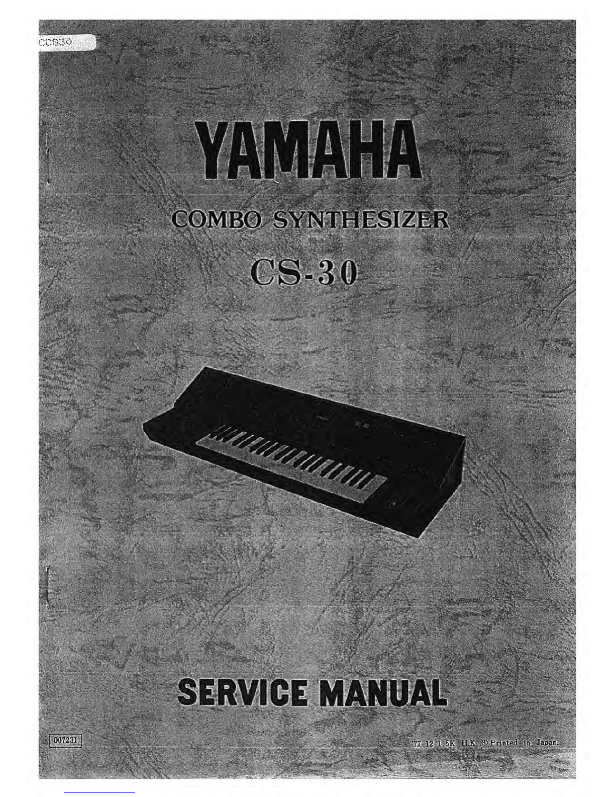
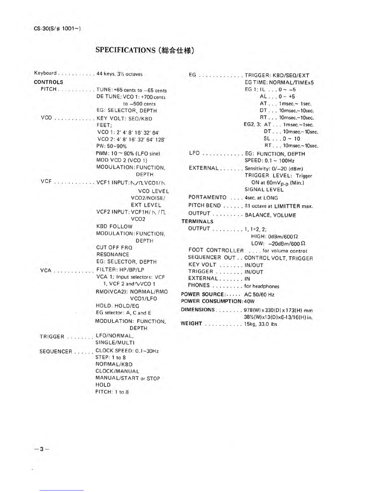
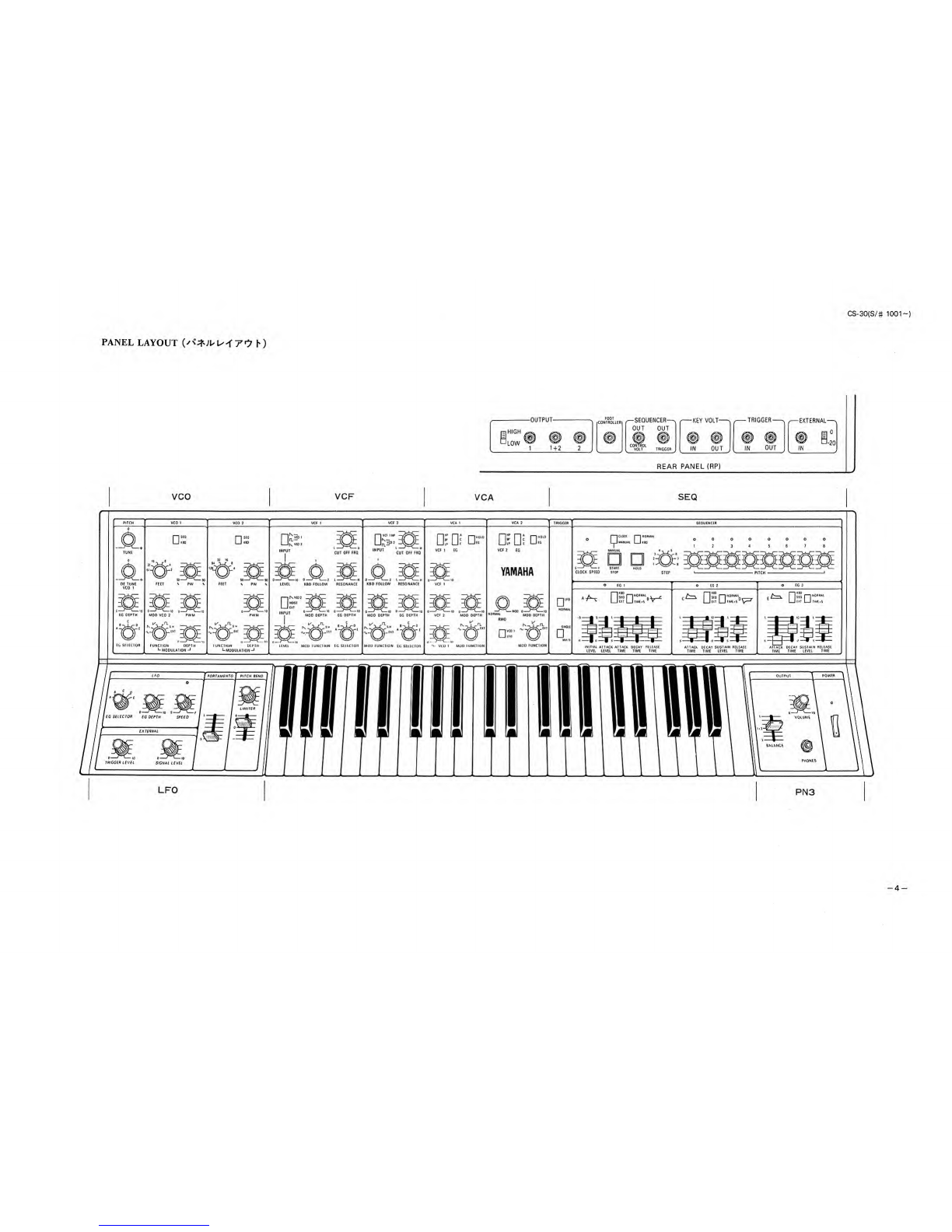
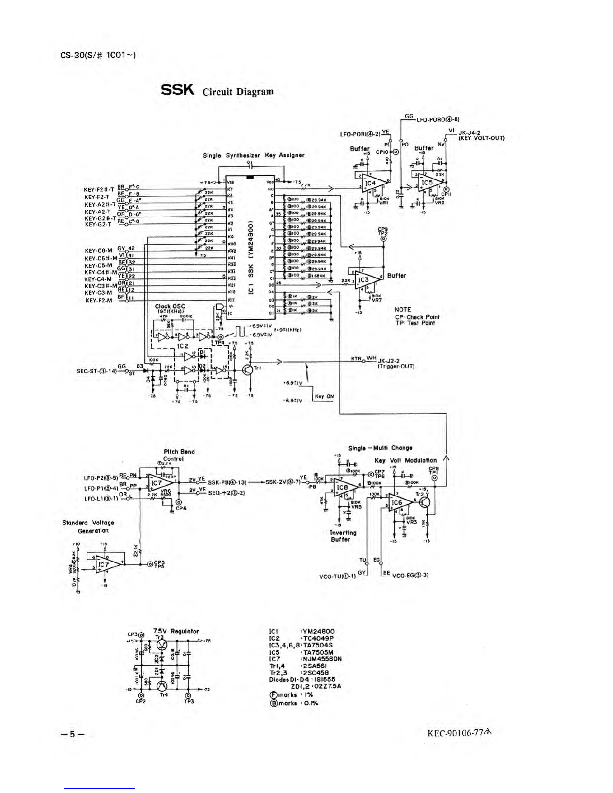
Yamaha CS-30 User manual

CC830
-’77.12
'1.5K
5S5322<
•f
*
v
'^
fV
t
A
14
'
■

CS-30(S/#
1001
~)
INDEX
(S
2fc)
CORDING
GUIDE(*JB«>¥5I)
.1
DISASSEMBLY
PROCEDURE^#^*).2
SPECIFICATIONS^^:*)
.3
PANEL
LAYOUT!'***
KTO!)
.4
SSK
Circuit
Diagram
(SSK->—
10
)
.
5
SSK
Circuit
Board
&
Wiring
(SSKx-
1
*t&0)
.6
VCO
Circuit
Diagram
(VCO->-
IE).
7
VCO
Circuit
Board
&
Wiring
(VCO->-
1
**0)
.8
VCF
Circuit
Diagram
(VCF->
—
10).
9
VCF
Circuit
Board
&
Wiring
(VCF->-
1**50).
10
VCA
Circuit
Diagram
(VCA->-
M
2
).11
VCA
Circuit
Board
&
Wiring
(VCA->-
1
*
*50)
.12
SEQ
Ciruit
Diagram
(SEQv—
1
0
)
.13
SEQ
Circuit
Board
&
Wiring
(SEQ->-
1**50)
.
1
4
LFO
Circuit
Diagram
(LFO*>—
10)
.
1
5
LFO
Circuit
Board
&
Wiring
(CFO->-
1**50)
.16
PRA
Circuit
Diagram
(PRA->-
10
)
.
17
PRA
Circuit
Board
&
Wiring
(PRA->-
1**50)
.18
ADC
Circuit
Diagram
(ADCx—
10
)
.
1
9
ADC
Circuit
Board
&
Wiring
(ADC->-
1
**50)
.
1
9
KEY
SWITCH
Circuit
Diagram
(*«->-
10).20
PN3
Cricuit
Diagram
(PN3->—
10).20
REAR
PANEL
Circuit
Diagram
(
9
7-'<*Jl>'>-
10)
.21
REAR
PANEL
Circuit
Board
&
Wiring
(9
1
**50).21
Standerd
for
circuit
inspecpion
and
adjustment
('>—
l**SP8*iJQ.22~37
PARTS
LIST
(''-7
9X1)

CS-30(S/
#
1001—)
CORDING
GUIDE
|)
O
CIRCUIT
BOARD
AND
WIRING
Two
(2)
black
wires
are
connected
to
“E"
on
circuit
board.
One
goes
to
each
**E*’
terminal
of
A
and
FG
circuit
boards.
In
this
case,
the
coding
system
is
as
follows:
Circuit
board
mE
BL12
x 2
[The
pattern
shows
the
view
from
the
side
parts
mounted)
Color
of
wire.
Number
of
stands
contained
in
the
core.
(In
case
of
8
cores,
the
number
is
not
shown.)
Number
of
wires.
RA-A-EI2)
RA-FG-EI2)
Terminal
point
physical
eyelet
space
location
•
Terminal
reference.
•Unit
(Board).
•
Rack
general
physical
location.
Terminal
point
shown
on
the
board.
(Solder
eyelet
space
number)
I—
Terminal
E
shown
on
the
board.
SYMBOL
DESCRIPTION
Transistor
FET
E
C
B
•
E3S
D
G
S
|BB*1
E:
Emitter
C:
Collector
B:
Base
S:
Source
G:
Gate
D:
Drain
Capacitor
—lh~
Electrolytic
capacitor
Polarity
Amark
:
Tantalum
capacitor
NP
mark:
Nompolar
capacitor
Myler,
Ceramic
and
Polystyrene
Capacitor
Diode
(Zener
Diode)
ABBREVIATIONS
OF
WIRE
COLOR
IN
ELECTONE
Switch
OB
OT
OM
B:
Break
T:
Transfer
M:
Make
BLACK
.
.BL
BROWN
.
.BR
RED...
RE
ORANGE.
.OR
YELLOW.
...YE
GREEN
GR
BLUE.
.
BE
VIOLET....
VI
GRAY
GY
WHITE
.
.
WH
GRASS
GREEN.
••••••
»
■
.GG
SKY
BLUE
..
SB
PINK
.
.
PK
TRANSPAPENT
....
.TR
Q
WIRE
COLOR
-
Musical
Note
Indication
C
C#
D
I
I
I
BR
RE
OR
D#
E
F
I
I
I
YE
GR
BE
F=
G
G#
A
A#
B
I
I
I
I
I
I
VI
GY
WH
GG
SB
PK
LOGIC
SYMBOL
fMILn
YAMAHA
NOT
A"O-Y
A-0"<
NOR
NAND
SO-
Exlusive
OR
Truth
Table
_
A
B
Y
0
0
0
1
0
1
0
1
1
1
1
0
NOT
(Inverter)
Truth
Table
A
Y
0
1
-J_
_Q_
OR
Truth
Table
A
B
Y
0
0
0
1
0
1
0
1
1
1
1
1
NOR
'.O'
Truth
Table
A
B
Y
0
0
1
1
0
0
0
1
0
1
1
0
AND
Truth
Table
A
8
Y
0
0
0
1
0
0
0
1
0
1
1
1
NAND
::[•>'
Truth
Table
A
B
Y
0
0
1
1
0
1
0
1
1
0
0
0
-1
-

CS-30(S/ft
1001
—)
DISASSEMBLY
PROCEDURE
Removal
of
Panel
Remove
all
screws
illustrated
above
and
take
away
the
panel,
lifting
it
up
gently.
W)
9[ls
TTSt'o
Removal
of
Keyboard
After
removing
the
panel,
pulling
out
the
screws
as
shown
above
permits
rotating
the
keyboard.
Removal
of
Circuit
Boards
h<7)WL
Take
the
circuit
boards
away
gently
from
the
panel,
removing
each
volume
knob
and
hexagonal
nut
without
any
damage
or
scratch
on
the
panel.
A*
fri'Mca*
>J
0
A
WO
*
*
£:
A
UTTSt'.
-2-

CS-30(S/#
1001
~)
SPECIFICATIONS
Keyboard.44
keys,
3'/
2
octaves
CONTROLS
PITCH.TUNE:+65
cents
to
-65
cents
DE
TUNE;
VCO
1:
+700cents
to
-500
cents
EG:
SELECTOR.
DEPTH
VCO.KEY
VOLT:
SEQ/KBD
FEET;
VCO
1:
2'
4'
8'
16'
32'
64'
VCO
2:
4'
8'
16'
32'
64'
128'
PW:50-90%
PWM:
10-90%
(LFOsine)
MOD
VCO
2
(VCO
1)
MODULATION:
FUNCTION.
DEPTH
VCF.VCF1
INPUT:N/(TVC01/K
VCO
LEVEL
VC02/N0ISE/
EXT
LEVEL
VCF2
INPUT:
VCF1H/
f\
/
IT
VC02
KBD
FOLLOW
MODULATION:
FUNCTION.
DEPTH
CUT
OFF
FRQ
RESONANCE
EG:
SELECTOR.
DEPTH
VCA.FILTER:
HP/BP/LP
VCA
1;
Input
selectors:
VCF
1,
VCF
2
and-VVCO
1
RMO(VCA2):
NORMAL/RMO
VCOI/LFO
HOLD:
HOLD/EG
EG
selector;
A,
C
and
E
MODULATION:
FUNCTION,
DEPTH
TRIGGER.LFO/NORMAL,
SINGLE/MULTI
SEQUENCER.CLOCK
SPEED:
0.1
~30Hz
STEP:
1
to
8
NORMAL/KBD
CLOCK/MANUAL
MANUAL/START
or
STOP
HOLD
PITCH:
1
to
8
EG.TRIGGER:
KBD/SEQ/EXT
EG
TIME:
NORM
AL/TIMEx5
EG
1;
IL
.
.
.
0~
-5
AL
.
.
.
0
-
+5
AT
.
.
.
1msec.-
Isec.
DT
.
.
.
10msec.~10sec.
RT
.
.
.
10msec-lOsec.
EG2,
3;
AT
.
.
.
1msec.~1sec.
DT
.
.
.
10msec.~10sec.
SL
.
.
.
0
-
10
RT.
.
.
10msec.~10sec.
LFO.EG:
FUNCTION.
DEPTH
SPEED:
0.1
-
100Hz
EXTERNAL.Sensitivity:
0/—20
(dBm)
TRIGGER
LEVEL:
Trigger
ON
at
60mVp.p
(Min.)
SIGNAL
LEVEL
PORTAMENTO
....
4sec.
at
LONG
PITCH
BEND.±1
octave
at
LIMITTER
max.
0UTPUT
.
B
ALANCE.
VOLUME
TERMINALS
OUTPUT.1,
1+2,2;
HIGH:
Od8m/600£2
LOW:
-20dBm/600£2
FOOT
CONTROLLER
....
for
volume
control
SEQUENCER
OUT
.
.
CONTROL
VOLT,
TRIGGER
KEY
VOLT.IN/OUT
TRIGGER.IN/OUT
EXTERNAL.IN
PHONES.for
headphones
POWER
SOURCE:.
AC
50/60
Hz
POWER
CONSUMPTION:40W
DIMENSIONS.
978(W)x330(D)
x
173(H)
mm
38'/j(W)x1
3(D)x6-13/16(H)
in.
WEIGHT.15kg,
33.0
lbs
-3-

SEQ
TRIGGER
SEQUENCER
n
ao
“
n
L_JmANUAI
|—|
HOAMAI
•
HO
o
1
o
2
o
3
O
4
O
5
o
6
o
7
O
8
UAl
□
□
CLOCK
SPEED
SUM
HOLD
SlOf
STEP
PITCH
EG
1
EG
2
EG
3
□
WO
NO*Ml
QJS
n
-
0
*"
1
UT
□
s
rr%
1*1
LJ»*'4
□
n
,,o,,ui
m
i—i
tun.*
s*ai
□
INITIAL
ATTACK
ATTACK
OECAY
HillASE
LEVEL
LEVEL
TIME
TIME
TIME
ATIALX
DECAY
SUS1AIN
RELEASl
TIME
TIME
LEVEL
TIME
ATTACK
DECAY
SUSIAIN
RELEASE
TIME
TIME
LEVEL
TIME

ezooS&z*
CS-30(S/#
1001—)
Circuit
Diagram
ICI
‘YM240OO
[C2
•TC4049P
IC3,4,6,0
:
TA7504S
IC5
*TA7505M
IC7
:
NJM4550DN
Tf
1,4
‘2SA56I
Tr2,3
‘2SC450
Diode*DI-D4
-ISI555
ZDI.2
-02Z75A
0mork*
*
1
%
©mark*
5
0.1%
—
5
K
EC-90106-77A

100/16
.
G
#(OI
1C
ICI
IC2
103,4,6
IC5
IC7
Transisi
Trl
,4
Tr2,3
Resistoi
Diode
(
ZD1.2
D1
—4
Semi
va
V8K4-1

CS-30(S/#
1001
—)
JK-J5-2
(KEY
VOLT-IN)
VCF-KV(©-7)
vco
Circuit
Diagram
VCF-F1
KCD-6)
WH
GG
VCF-F10(©-10)
(PVR5)
-10
0Jo”ivcF-n.i(CD-3)
^O^VCF-M(0-1)
P^|o^-VCF-a2((i)-2)
^0-^-VCF-N2«D-12)
JK-J7-2
(SEQ
VOLT)
PK
VCF-EX3KD-14)
—
JK-SW1-T
<s«
(EXTERNAL)
—
VCF-S/H((D-10)
LFO-S/H(fi>10)
LFO
011(0)10)
VCF-NM)-4)
LF0-N((!)-8)
0*15
-15
EKO
-HOO-
-C-»'lO
'I
IEG
DEPTH
1
EG
SELECTOR
(PVR3)
LF0-A(fl>5)
BR
LF0-C(®-3|
ORr
'
>2)
VCF.C(®-B)^
-SSK-EGKD-12)
KFC-00107-78
A

CS-30(S/#
1001
~)
vco
Circuit
Board
&
Wiring
pvAio
B
iOk
*v(1
*
B
10K
17C0»
-41-
r-rm
wca
*
JK
%
4
0
—
*
—
1
—
*
.
i
13
13 .
n_
r~i_
J
S"'
_a
S/M
7
IXT
$
sxt
V
■
4
3
3
•V
1
View
from
the
printed
pattern
side
of
the
circuit
board.
(Note)
1.
1C
IC1.4
:
NJM4558DN
IC2,
3
:
TA7504S
IC6,
7
:
IG00153
IC8.9
:
IG00158
IC5
:
IG00151
2.
FET
FET1,
2
:
2SK30A
3.
Diode
D1,2
:
1N34A
D3,
4
:
1
SI
555
4.
Resistor
©marks
:
0.1%
©marks
:
1%
VCO
III
(IG00153)
This
1C
is
used
for
voltage
controlled
oscillator.
Many
defferent
frequencies
are
produced
by
the
vol¬
tage
supplied.
1.
FT.
Resistor
for
determination
of
the
feet.
The
electric
current
is
provided
to
the
pin
from
transposition
changing
circuit
so
that
the
octave
can
be
determined.
2.
KV
.
Input
of
the
key
voltage
The
input
of
the
voltage
is
provided
to
the
pin
in
corporation
with
the
keys
held
down.
High
voltage
High
frequency
Low
voltage
Low
frequency
(ex,)
Transposition
"normal"
OFF-SET
....
Zero
adjustment
of
input
4.
/
buffer
circuit
5.
Vee
.
-15V
input
power
source.
6.
Com
....
Phase
compensation
for
input
buffer
amplifier.
Normally,
the
output
(KV
♦
IV)
is
supplied
to
the
pm.
7.
OUT
....
Output
3.5V
pp
8.
GNO
Earth
9.
Vref
.
Input
of
the
standard
voltage.
10.
CT
.
Circuit
for
lime
constant.
As
to
the
frequency,
refer
to
the
Pin
No.2
(KV).
Input
Voltage
Output
Frequency
0.250V
130.8Hz
(C2)
0.500V
261.6Hz
(C3)
1.000V
523.2Hz
(C4)
2.000V
1046.0Hz
(C5)
4.000V
2093.0Hz
(C6)
The
following
wave
shape
is
produced.
11.
RT
.
Circuit
for
time
constant.
t
Determines
the
discharging
voltage
level.
12.
T1.
Input
for
the
comparator.
Input
of
the
wave
shape
(|\J\J
)
is
provided,
from
the
pm
no.
14
(TO).
13.
Iref
.
Input
of
the
standard
electronic
current
14.
TO
.
Output
from
time
constant
circuit.
The
following
wave
shape
is
produced.
15.
VIB
.
Input
for
vibrato
control
wave.
16.
Vcc.
+
15V
input
power
source.
WSC
1C
(IG00158)
1.
Vcc
2.
SIO
3.
TO
4.
SL
♦
15V
input
power
source
Output
of
the
sine
wave
Output
of
triangular
wave.
~AA
A°
p
Input
of
slice
level.
Input
of
the
DC
voltage
is
provided
to
the
pin
for
determination
of
the
inverting
level
which
makes
triangular
wave
from
sawtooth
wave.
Triangular
wave
—Slice
level
:
Sawtooth
wave
5.
S5.
Output
of
the
inverter
wave
Output
of
inverted
sawtooth
wave
is
produced.
/
Sawtooth
wave
Inverted
sawtooth
wave
6.
2TO
.Output
of
double
triangle
wave
Double
triangle
wave
is
produced
from
triangle
wave.
7.
PO
.
Output
of
pulse
wave.
in.
8.
Vee
.-15V
input
power
source.
9.
PI
.Input
of
pulse
wave
Input
of
sawtooth
wave
is
provided.
hvNJX
rUTTL
10.
PWO
.Output
of
OP
amplifier.
11.
PWI
.Input
of
OP
amplifier.
rvw
nuiim
nrlru
Input
of
the
voltage
is
pro¬
vided
for
determination
of
the
sensitivity
of
PWM
lever
so
that
the
pulse
width
is
changed.
12.
2TI
.
Input
of
triangular
wave
for
produc¬
ing
double
triangular
wave
shape.
A/V
,T0
'“
double
shape.
wave
13.
5T
.
Input
of
the
pulse
for
producing
in¬
verted
sawtooth
wave.
Input
of
the
sawtooth
wave
is
provided
from
VCO
HI
for
producing
inverted
saw¬
tooth
wave
shape.*
NN\
14.
Tl
Input
of
the
wave
is
provided
for
producing
triangular
wave
shape.
15.
STI.
Input
of
the
wave
for
producing
sine
wave.
Input
of
the
triangular
wave
(TO)
is
provided
for
pro¬
ducing
sine
wave.
16.
GND.Earth
KEP-NA80289-78
A
-
8
-

CS-30(S/
#
1001—)
VCF
1C
(IG00156)
1.
A!
2.
KV
3.
fc
4.
Vf
5.
Vcc
6.
QO
7.
VQ
.
8.
GNO
9.
FB
..
10.
LP
.
11.
C2
.
12.
Vee
13.
BP
.
14.
Cl
..
15.
HP
16.
IN
.
...
Signal
Input
Input
signals
from
VCO
are
provided
to
this
pin.
....
Key
voltage
input
In
order
to
change
the
tone
color
according
to
the
tone
range
of
key¬
board,
the
degignated
voltage
of
the
key
will
supplied
to
the
pin.
(0.25-
4.0V)
....
Adjustment
of
the
cut
off
frequency.
Set
the
control
currency
of
the
cut
off
frequency.
...
Input
of
the
cut
off
voltage.
Input
voltage
of
cut
off
frequency
is
supplied
to
this
pin
so
that
the
tone
color
can
be
changed.
The
center
point
of
the
cut
off
frequency
can
be
also
set.
When
the
VK
is
0.25V
and
Vf
is
5V.
the
cut
off
frequency
is
set
to
just
1
KHz.
.
+15V
input
power
source
....
Q
adjustment.
The
Q
control
current
sets
the
Q
equal
to
1
0.
when
VQ
is
0
volt.
...
Input
of
the
voltage
for
Q
control.
Q
is
variable
according
to
the
control
voltage
supplied.
When
the
control
voltage
is
0V
(Max.),
Q
s
10
When
the
control
voltage
is
10V
(Min.),
Q'0.5
....
Earth
.
Q
feed
back
This
is
the
feed
back
output
pin
for
the
Q
control
by
which
the
Q
is
determined.
.
Low-pass
output
I
-6dB/OCT
L
™
.
The
output
o*
lower
fre-
quencies
are
produced.
C
pin
for
determination
of
the
cut
off
frequency.
—
15V
power
source.
Band-pass
output.
dB/OCT
►
The
output
of
intermediate
frequences
are
produced.
C
pin
for
determination
of
the
cut
off
frequency.
Hi-pass
output
+6dB/OCT
The
output
of
higher
fre¬
quencies
are
produced.
Input
of
feed
back
The
input
signal
for
determination
of
cut
off
frequency.
-Explanation
for
1C
(
I
CttW)
VCF
Circuit
Diagram
VCO-KF1
ua>-2)-^
GG_
vCQ
.
kf
,
ofQ.5,
FII
FIO
[input]
(PSWI)
I-1
VR2
eiooK
VCF
I
vco-
MKD-6)
BR
_
N|
I
i.
vco-aiK3>-7)^i<>0^—
'So
LFO-NiKD-n
VCF-EXT(fS)-12)££o^
VC0-EXT«ft)-7)
i
r-
s
22
OK
TP4
I
.
®
TP2©-4
*58
L
_T-iL
-I-
VCO-N2(®-3)
VCO-n2(©-4)
VCF
VE
q
K2
GG
H
2
ilevelI
(PVR2)(
PVRI)
c
KB0
FOLLOW
MiJIi
(PSW3)
r;F
(PVR3)
!RES0NANCEl
[
(PVR5)
(PVR71
r
~ir
‘P
i
Y
i
1
X
I
i
1
2|-
1
j
“T
1
1
__J
1
...
VPI_
B200K
1
•
-
1
1
■
^
*
h
1>
1
,
t
r
00
Cl
C2
GNO
MK
4
7M
NP
OOOI5
-i^o^-vcA-HPtKD-D
BPUGY
VCABPttCD-9)
VC
A-H
P1
(CD-
10)
Oi
—T—J
(PSW4)
(PVR9)
LECTOR
[depth
I
i
270K
-
Buffer
vco-Kvro.gj
VI
kv
150-
V
(o)TPI
Buffer
TP5
(o)
TP3
«k>
r
-
0*15
1
2=
I-
-T-'
L
-Y-!
L_Y__
►
-15
KBD
FOLLOW
(PVR6)
(PVR4)
(PVR8)
8=
(PSW6)
(PVRII)
•15
VCF
2
220K
&
S
•15
*
St®
C^3
l^o
2
IOK
a
If
M
^
""In
HP
*
v
(0
nr
rc
*0
Ci
V,
g
BP
Uf
f
vcc
u
00
C
VTc
C2
VO
3
IP
GNO*
-
r
B
•6
0
0015
820K
0
0015
10/16
-lb
HP
HP2^GG
VCA-HP2(CD-n)
I0M6
ffiTP
T-
si
i^O^-VCA
BP2|fi>13>
VCALP2((0-12)
LP2
rt
PK
LI_J
MOD
SELECT
EG
EG
SELECTOR
DEPTH
(PVR
10)
(PSW7)
(PVRI2)
.*10
VCO-KF2H0-7)
VC0-KF20f0
6)
F20
VC0-*v(®-2)-
VCA-M<2)-2)
VCO-K
«Ci)-4)
•
VCA-NW)-3)
VC0.^(f«)13»-
ICI
,2=
IG00I56(A)(8)(C)
IC3.4
*
NJM4558DN
Rl.2,3,4
Rank
RI.R2
A
30K
,
470
B
1
2.4
K
430
C
1
20
K
390
WH
GG
VCOTUSM)
VCA-ap^-5)
SB
VC0-S/H{d>9)-
OR
PN3-PL-2
PN3-PL-1
VCF-EXS(®-15)-
VCA-EXT((2>-7)
PK
—^-SEQ-BM»-3)
VCO-B((5)-6J
•VCA-At(D-2)
VC0-A(®3)
VCA-E(®-6)
VCO-EtdM
1)
SEQOfl)-6)
VC0DP»)-9)
VCACPD-4)
VC0-CfS»-7)
-15
-9-
KEC-90108-78
A

VCF
Circuit
Board
&
Wiring
*vn?
a
wk
•
m*rk
:
CS
301
only
*
m*/k
:CS-30oni
v
View
from
the
printed
pattern
side
of
the
circuit
board
(Note)
1.
1C
IC1,2
:
IG00156
IC3.4
:
NJM4558
2.
Resistor
®
marks
:
±
1
%
R1R2R3R4:
Rank
of
IC1,2
1C
Rank
R1R2
R3R4
/
Q
•3
1?
IXT
CXT
~i~
S/H
»
3
0
-
Q
1
:
HU-
jlol
i
'
*
KEP-NA
80290-78A
CS-30(S/#
1001—)
VCF-EG
(IG00152)
This
1C
generates
envelope
wave
shape
which
is
supplied
to
VCF
and
control
the
tone
color.
1.
NC
.
Not
connected
2.
Bl
.
Input
of
buffer
amplifier.
3.
OUT
....
Output
of
buffer
amprifier.
The
buffer
amplifier
is
built
in
for
the
purpose
of
matching
inpedance.
Output
wave
shape
T
7
"
'
AL
1
-H-v
It:/
KEY-ON
-
AT
-w««DT*,
-H
I
SL
KEY-OFF
4.
GND
....
Earth
5.
Vcc
.
+15V
input
power
source.
6.
G1
.Gate
1
7.
G2
.Gate
2
8.
Vee
9.
AT
AT
starting
data
Key
ON-OFF
data
-15V
input
power
source.
Input
of
buffer
voltage
for
determi¬
nation
of
the
attack
time.
Input
of
the
voltage
between
zero
V
and
10V
is
provided
and
the
attack
time
is
controlled
from
1
mS
until
IS.
ur
AT
0
10.
DT
Input
of
buffer
voltage
for
determi¬
nation
of
the
decay
time.
Input
of
the
voltage
between
zero
V
and
10V
is
provided
and
the
first
decay
time
is
controlled
from
10mS
until
10
S.
IDT
11.
RT
Input
of
buffer
voltage
for
determi¬
nation
of
the
release
time.
Input
of
the
voltage
between
zero
V
to
10V
is
provided
and
the
time
from
KEY-ON
until
release
is
con¬
trolled
from
10
m
second
until
10
second.
KEY-OFF
12.
TC
.
Output
of
the
time
control.
Output
of
DC
voltage
is
produced
so
that
the
each
time
of
attack,
DT
and
RT
are
controlled.
I
A
!
11
Time
control
voltage
The
higher
the
voltage,
the
shorter
the
time
and
the
lower
the
voltage
the
longer
the
time.
13.
LC
.
Output
of
level
control.
+
5
y_^
Output
of
DC
voltage
in
produced
so
that
the
IL
and
AL
is
-5V
level
control
voltage
+5V
-0
-
—5V
The
higher
the
voltage,
the
higher
the
level
and
the
lower
the
voltage
the
lower
the
level.
14.
AL.
Input
of
butter
voltage
for
determi¬
nation
of
attack
level.
Input
of
the
voltage
between
(0V~
10V
is
provided
and
the
attack
level
is
controlled
from
0V
until
+5V.
15.
SL
Input
of
buffer
voltage
for
determi¬
nation
of
the
sustain
level.
Normally
fixed
to
zero(0)
volt.
+5V
-5V
16.
IL
.
Input
of
buffer
voltage
for
determi¬
nation
of
the
initial
level.
Input
of
the
voltage
between
zero
0V
and
ten
10V
is
provided
and
the
initial
level
is
controlled
from
zero
to
minus
5
volt.
-10-

CS-30(S/#
1001-)
--Explanation
for
1C
(
I
ClftBfl)
VCA
Circuit
Diagram
VCA
1C
(IG00151)
1.
El
.
Input
voltage
for
level
control.
Input
of
the
control
voltage
is
pro¬
vided
for
changing
the
level
expotenen
tiolly.
2.
L
I
.
Input
of
level
control
voltage.
Input
of
the
control
voltage
i$
pro¬
vided
for
linear
change
of
the
level.
Input
LI
wave
0
dB
out
3.
+
IN
.
Input
Input
of
the
level
modulated
signal
is
provided.
shape
INPUT
OUTPUT
4.
-IN
.
Negative
feed
back.
Normally
unused.
5.
Vee
.
-15V
input
power
source.
6.
Vcc
.
+15V
input
power
source.
7.
GND
.
Earth
8
OUT
.
Output
Output
Wave
Shape
Output
of
the
following
wave
shape
is
produced.
-ii
-
KEC-90109-78
A

VCA
Circuit
Board
&
Wiring
PSW7
PSW9
100/16
100/16
PVR3
A-50K
470K
10/16
100K
PVR5
B-10K
100/16
PVR2
A-50K
PVR
|
A-50K
>
PSW6
100K
(Note)
View
from
the
printed
pattern
side
of
the
circuit
board
'<9
IC1
—4
:
IG00151
IC5
:
NJM4558
IC6
:
HA1452
IC7
:
/iA796HC
2.
Transistor
(
h
=7
>\s7*
9)
Trl-5
:
2SC458
3.
Phote
coupler
PCI
•
2
:
P558-G50-201B
4.
Semi
Variable
Resistor
UR1
-9
:
V8K-4-1
Type
)
15
G
»
M
G
JIT
G
)1
12
G
)l
11
G
)|
10
G
)|
9
G
3jl
G
■
)
4
02
»
3
G
|
2
■
!
-L
♦
10
KEP-NA
80291
-78
A
CS-30(S/#
1001
VCA-EG
1C
(IG00159)
This
1C
generates
envelope
wave
shape
which
is
supplied
to
VCA
and
control
the
tone
volume.
1.
IL
.
Input
o*
initial
level-
Fixed
to
0V
2.
Bl
.
3
OUT
...
Input
of
buffer
amplifier.
The
buffer
amplifier
is
built
in
for
the
i
hi
ipose
of
matching
mpedance
Output
wave
shape.
DT
K
AT
4.
GND
.
Earth
5.
Vcc
.
*15V
input
power
source.
6.
G1
.
Gate
1
7.
G2
.Gate
2
KEY
ON
/V
KEY-OFF
0V
2»
■
1
_
AT
starting
data
Key
ON
OFF
data
8
Vee
.
♦
15V
input
power
source.
9
AT
.
Input
of
buffer
voltage
for
determi¬
nation
of
attack
time.
Input
of
the
voltage
between
zero
V
and
10V
is
provided
and
the
attack
time
is
controlled
from
1
mS
until
IS
k
ATM
10.
IDT
.
Input
of
buffer
voltage
for
determi¬
nation
of
decay
time.
Input
of
the
voltage
between
zero
V
and
10V
is
provided
and
the
decay
time
is
controlled
from
10
m
second
until
10
second.
11
2DT
.
Input
of
buffer
voltage
for
determi¬
nation
of
release
time.
Input
of
the
voltage
between
zero
V
and
10V
is
provided
and
the
time
key-off
untill
release
is
controlled
from
10
mS
until
10
S.
12.
TC
.
Output
of
time
control.
Output
of
the
DC
voltage
is
pro¬
duced
so
that
the
each
time
of
Attack.
1st
Decay
and
2nd
Decay
are
controlled.
KEY-ON
i
OFF
Tune
control
voltage
The
higher
the
voltage,
the
shorter
the
time
and
the
lower
the
voltage,
the
lon¬
ger
the
time.
13.
LC
.
Output
of
level
control
Level
control
voltage
Output
of
the
DC
voltage
for
AL
and
SL
control
is
provided.
The
higher
the
voltage
.
the
higher
the
level
and
the
lower
the
voltage,
the
lower
the
level.
14.
NC.Not
connected.
15.
SL.
Input
of
buffer
voltage
for
determi¬
nation
of
the
sustain
level.
Input
of
the
voltage
between
zero
V
and
10V
is
provided
so
that
the
sustain
level
can
be
controlled.
10
0
16.
NC.
Not
connected.
-
12
-

CS-30(S/#
1001—)
Circuit
Diagram
Genelotor
I
Buffer
*oo.
SSK-
+
7.5((2)-7)
SSK-ST(®-1)
.ft
fi«2»
ose
CPVRI)
TP?
i
i
urn
e
u«»
Vft
wh
a
vcoa
Tf2
Schmitt
Trigger
W-O
\Tr26
(PSWI)
™
••
40-0^-
IC2
•
I5*plnl4
GN0*pln7
V*
'
ter
IPSWIO)
Sfor»-S»op
Control
\y
TART]
^
,
s
_
L
JOPj
--
o*o
J
,K
IJiM
•
90-
■
IS
•
-
<
-ta
:
•»
z
i
.
*
:
i
*
**
'
9
ITrK)
a.
el
?
ml
Tr
13
Cf
0*
IC3
r
■■
■
»
PILOT
LAMP
VCF-G((D
VCF-PL(®-I3)
n
i
>*
NOR.
•
•
&
•*
J
•
4f*
X
3
r
*
(PSW*.
>
!
j
ry.
s
.
(PSW4I
It
LEI
LE2
LE3
LEA
LE5*
L£6
LE7
LE8
—
^
—
••
—
“
■
•
*
••
•
•
•
••
*
••
™
•
••
•
■■
••
^
•
•
.AJlAAJlJl
yijK-J6-2
TR
(SEQ-Trigger
OUT)
Tf«
-JT/|*
-jTr?0
._JTf2l
T»22
^-jTr23
^jTf24
_.Tr25
g
r€)
Buffer
LEO
Orlver
xe
GoteXB
‘I
~
«'
■
'
‘‘l't
1
.
t
^ji
1
.
‘l
h-H
«.’
■
e
|e
-fiJ
IC6
•I3«pm»4
00
be
JK-J7-2
(EQ-VOLT
OUT)
f<2)T
P«
Schmitt
Trigger
^
4f*
-vi
rI----
-
!.
iMl
'-iiVINI
-ti-TLJI
ITil-iTJ
eircHel
l
-—
(PVR2)
(PVR3)
(PVR4)
IPVR3)
(PVR6)
(PVR7)
(PVR8)
(PVR9)
IC3
♦
I5»pinl4
GNO
’pin
7
(PSWII)
KV
2V
JK-J5-2
(KEY
VOLT-IN)
LF0-LTR(3)-7)
JK-J3-2
(Trigger-IN)
(PSW2
U2)
RE
LFT
—
->
•••
Invertor
A
%
_
•*
J
jk
»o—
QLleo?.
(O
«T
n
LEO
r
(PVRI2)
(PVRI3)
Envelope
Genelotor
2
mm
(PVHI4)
Tf
2»
Driver
•0
?r*
"
it
1
'...
MM
u
Hifcl
!
(PVRI7)
Invertor
*
TP4
5;
!
mm
Tf
29
lLEDIO
(PVRI3)
Envelope
Genelotor
3
ill
il
•
(PVR2I)
it
•CH
4
7*
in
r"H‘
VCA-A(G>-3)
K*»
0*F
VCA-C(®*5)
«nON
K^orr
K>
orooi
VCF’Df&ll)
*V°*'
(
7
OM
’AT
OT
«T
-1
lOtOOl
iofiS.
VCA-EKD-7)
otooi
bot-
tit
.»
•»
PSW6)?
MM
SSK-2VfD-
*
)
YE
+
15-
LF0-N(®-2)
;
LFS
1C
TP
j-Lfio*
->
I
r
-r
LFO-ETOfD-5)-^
Tr
3l
LklfS'J
2
EC
!&
,oj
(PVR22I
ICI3.I4
LED
Driver
'
1G00I30
TC4069P
1
TC40I
IP
•TC4022P
-TC40I6P
1
TA7303M
•TA7504M
■
IG00I3I
1
IG00IS2
•IGOOI39
103,16
NJM4338DN
Tr6,l7
1
2SAS6I
Tr7~l6j8-32'2SC458
I'S
KEC-90111-78
A

CS-30(S/#
1001
—)
SEQ
Circuit
Board
&
Wiring
\\\V
PVR15
PVR22
B-10K
HOLD
TR
PVR3
B-10K
YAMAHA
X82630
>
3/
8
YAMAHA
lC82630
View
from
the
printed
pattern
side
of
the
circuit
board
'
<
*
-
>
m
»
*
b
H
&
K
«
T
t
o
(Note)
1.
1C
2.
Transistor
(
IC1
:
IG00150
Tr6,17
:
2SA561
IC2
:
TC4069P
other
:
2SC458
IC3
:
TC4011P
3.
FET
:
2SK30A
IC4
:
TC4022P
4.
Diode
K)
IC5,6
:
TC4016P
D
:
1S1555
IC8
:
TA7504M
5.
LED
K)
IC9
—11
:
IG00151
SLP1328
IC12
:IG00152
IC13,14
:
IG00159
IC15,16
:
NJM4558
IC7
:
TA7505M
—
14
—
KEP-NA
80293-78
A

CS-30(S/#
1001—)
LFO
Circuit
Diagram
PITCH
BEND
PVR7)
(PVR6)
[PORTAMENfol
(PVR5)
'
1
—
1
1
:C
i
a
:
C>—:
■
Cl
I
f
<
1
1
•
%
—
?-->
SSK-P0(CD-2)
AMP
External
Trigger
SE-ETR(fD-13)
-15-
KEC-90112-78
A

CS-30(S/£
1001
~)
LFO
Circuit
Board
&
Wiring
•10K
10M-
0.039
FET2
View
from
the
printed
pattern
side
of
the
circuit
board
SE3SE
VCO
II
(IG00150)
1.
VI
2.
GND
3.
C
....
4.
Vee
5.
Vcc
6.
SIO
7.
SO
8.
ladj
Input
of
the
control
voltage.
The
frequency
is
variable
in
accord¬
ance
with
the
voltage
supplied.
VC1
Input
of
the
voltage
0-10V
'
is
provided.
Earth
Capacitor
for
determination
of
the
frequency.
-15V
input
power
source.
♦
15V
input
power
source.
Output
of
sine
wave.
zsz
3.20Vpp
Output
of
sawtooth
wave
3.5Vpp
Setting
for
standard
electric
current.
(Note)
1.
1C
IC1
:
IG00150
IC5
:
BA634
IC9
:
HA1452
IC2~4,
6~8
:
NJM4558
2.
Transistor
(
h
=7
9
)
Trl
~
9,
11,12,14,15,17,20
:
2SC458
Tr10,13,16,18,19
:
2SA561
3.
Diode
(5^*-
K)
D
:
1
SI
555
ZD
:
1
SI
715
4.
FET
PET
1,2
:
2SK30A
KEP-NA80294-78
A.
-16-

CS-30(S/£
1001—)
PN3-VA2A-2
(Volume)
PN3-VR2B-2
(Volume)
PRA
Circuit
Diagram
Pre-Amp(
I
)
♦
15
•JK-J8-4
(Foot
Controller)
-17-
KEC-90110-78
A

Circuit
Board
&
Wiring
©
8H32-5IHT
W
0S3S83J
AHAMAY
®
(Note)
1.
1C
IC1,2
:
HA1452
2.
Transistor
(
Y
7
Trl
,5,6
:
2SC458
Tr2,9
:
2SD235
Tr3,7
:
2SA561
Tr4.8
:
2SA490
3.
Diode
4
X
—
V)
D1~13
:
1S1555
4.
Semi
Variable
Resistor
VR1,2
:
V8K-4-1
5.
Metal
oxide
film
resistor
*
marks:
mm
KEP-NA80292-78A
Other manuals for CS-30
4
Table of contents
Other Yamaha Synthesizer manuals

Yamaha
Yamaha JOGR JOGRR CS50 User manual

Yamaha
Yamaha CX5MII User manual

Yamaha
Yamaha SY-2 User manual

Yamaha
Yamaha SY-77 User manual

Yamaha
Yamaha P-120 P-120S User manual

Yamaha
Yamaha S-30 User manual

Yamaha
Yamaha MO6 User manual

Yamaha
Yamaha Electone GX-1 User manual

Yamaha
Yamaha MM6 User manual

Yamaha
Yamaha DX27 User manual

Yamaha
Yamaha YM3806 Manual

Yamaha
Yamaha DX27 User manual

Yamaha
Yamaha VCJ4330 User manual

Yamaha
Yamaha DX27 User manual

Yamaha
Yamaha DX27 User manual

Yamaha
Yamaha Portatone PSR-E313 User manual

Yamaha
Yamaha SY-35 User manual

Yamaha
Yamaha EX7 Instruction Manual

Yamaha
Yamaha PortaTone PSR-400 User manual

Yamaha
Yamaha DX7 II D Installation and operation manual