Xerox Dove Product manual

XEROX
Dove
lOP
Board
Technical
Reference
Manual
Version
1.2
July
1987

Dove
lOP
Board
Technical
Reference
Manual
Xerox
Corporation
Document
Systems
Business
Unit
Processor
Development
475
Oakmead
Parkway
Sunnyvale,
California
94086

Information contained in
this
manual
is subject to change
without
notice.
For
this
printing,
speaker
information was added. A revision
history
at
the
back
of
this
publication
lists
all
pages changed since
the
First
Edition.
The
last
page
of
this
publication
is
a
Reader
Comment
form.
Comments
are
welcome
and
become
the
property
of
Xerox
Corporation.
This
publication
was
produced
using
ViewPoint
on
a
6085
Professional
Computer
System,
printed
on a Xerox 8040 RAVEN
laser
printer,
and
reproduced on a Xerox 9900 High Speed Copier.
Copyright
co
Xerox Corporation 1985, 1986,
and
1987.
XEROX @ ,
ViewPoint,
6085, 8040,
and
9900
are
trademarks
of
XEROX CORPORATION.
No
part
of
this
publication
may
be reproduced
or
translated,
stored
in
a
database
or
retrieval
system,
or
transmitted
in
any
form
or
by
any
means,
electronic, mechanical, photocopying, recording,
or
otherwise,
except
as
expressly
permitted
by Xerox Corporation.
Printed
in
the
United
States
of
America
.

P.I
Purpose
P.2
Audience
p.a
Organization
P.4
References
Preface
The
lOP
Technical Reference
Manual
describes
the
hardware
on
the
Dove
lOP
board. The
manual
describes
the
theory of
operation
of
the
components,
and
presents
information
important
for
programmer
interface.
The
following groups
are
expected to refer to
this
publication:
Engineers
Systemdesigners
Microprogrammers
Field Service personnel
Mter
a
brief
overview, each major
part
of
the
lOP
board is discussed
in
a
separate
section. Components'
are
described
as
to
hardware,
theory
ofoperations,
and
programmer
interface.
Hardware
describes pins
and
signals
of
the
component.
Theory
of
Operations describes
system
operating
modes, which
may
include timing.
Programmer
Interface describes
register
assignments
and
timing.
An
addendum
describes
the
speaker.
Appendices contain
supplementary
information
about
the
board
and
components. Because
this
manual
corresponds to B2
and
later
builds
ofmachines,
earlier
machines
will have some differences. Appendix C
lists
the
documentation
that
describes
the
various
issued
lOPs
found
in
the
Dove machines. Appendix
D,
reprinted
in
a
separate
volume,
contains
a
representative
set
of
schematics.
The
following documents
contain
supplementary
information.
AMD 2942 Specification Sheet. Bipolar Microprocessor
Logic
and
Interface 1985
Data
Book,
Advanced
Micro
Devices, Sunnyvale, CA

Dove
lOP
Board
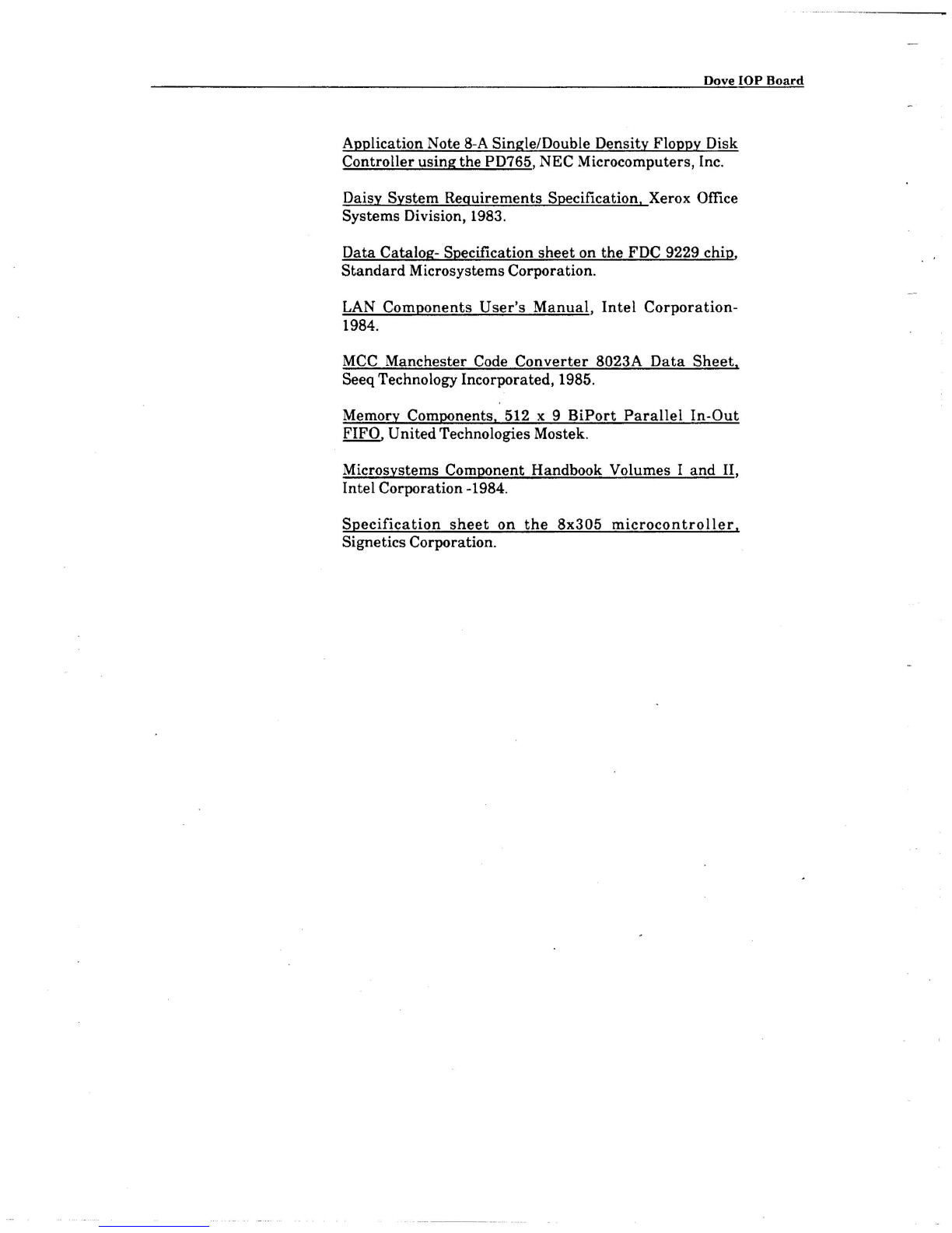
Application Note 8-A SinglelDouble Density Floppy Disk
Controller using the PD765, NEC Microcomputers, Inc.
Daisy System Requirements Specification. Xerox Office
Systems Division, 1983.
Data
Catalog- Specification
sheet
on
the
FDC 9229 chip,
Standard
Microsystems Corporation.
LAN
Components
User
's
Manual,
Intel
Corporation-
1984.
MCC
Manchester Code
Converter
8023A
Data
Sheet.
SeeqTechnology Incorporated, 1985.
Memory Components. 512 x 9
BiPort
Parallel
In-Out
FIFO,
United
Technologies Mostek.
Microsystems Component Handbook Volumes I
and
II,
Intel Corporation -1984.
Specification
sheet
on
the
8x305
microcontroller.
Signetics Corporation.

TABLE OF CONTENTS
1.
lOP
Board
1.1 Overview
1.2
Hardware
1.2.1
Printed
wiring
board
assemblies
(PWBA)
l.2.2
Interfaces to
backplane
l.2.3
Power
2.
110
Processor
and
Related
Components
2.1
Hardware
2.1.1
Chip
and
chip socket
2.l.2
Pin
assignments
and
description
2.2 Theory
of
Operations
2.2.1 Execution
unit
2.2.2
Integrated
DMA
unit
2.2.3
Integrated
timer
unit
2.2.4
Integrated
interrupt
controller
2.2.5 Clock
generator
2.2.6
Chip
select
unit
2.2.7
Integrated
peripheral
accessing
2.3
Programmer
Interface
2.3.1 Processor
reset
and
initialization
2.3.1.1 Local
bus
controller
and
reset
2.3.l.2
Chip
select/ready
logic
and
reset
2.3.l.3
DMA
channels
and
reset
2.3.l.4
Interrupt
controller
and
reset
2.3.l.5
Timers
and
reset
2.3.2
Chip
select
address
and
register
bit
maps
Table
of
Contents
1-1
1-3
1-3
1-6
1-8
2-2
2-2
2-3
2-7
2-7
2-8
2-9
2-10
2-10
2-10
2-11
2-12
2-12
2-12
2-13
2-13
2-13
2-13
2-14

Dove
lOP
Board
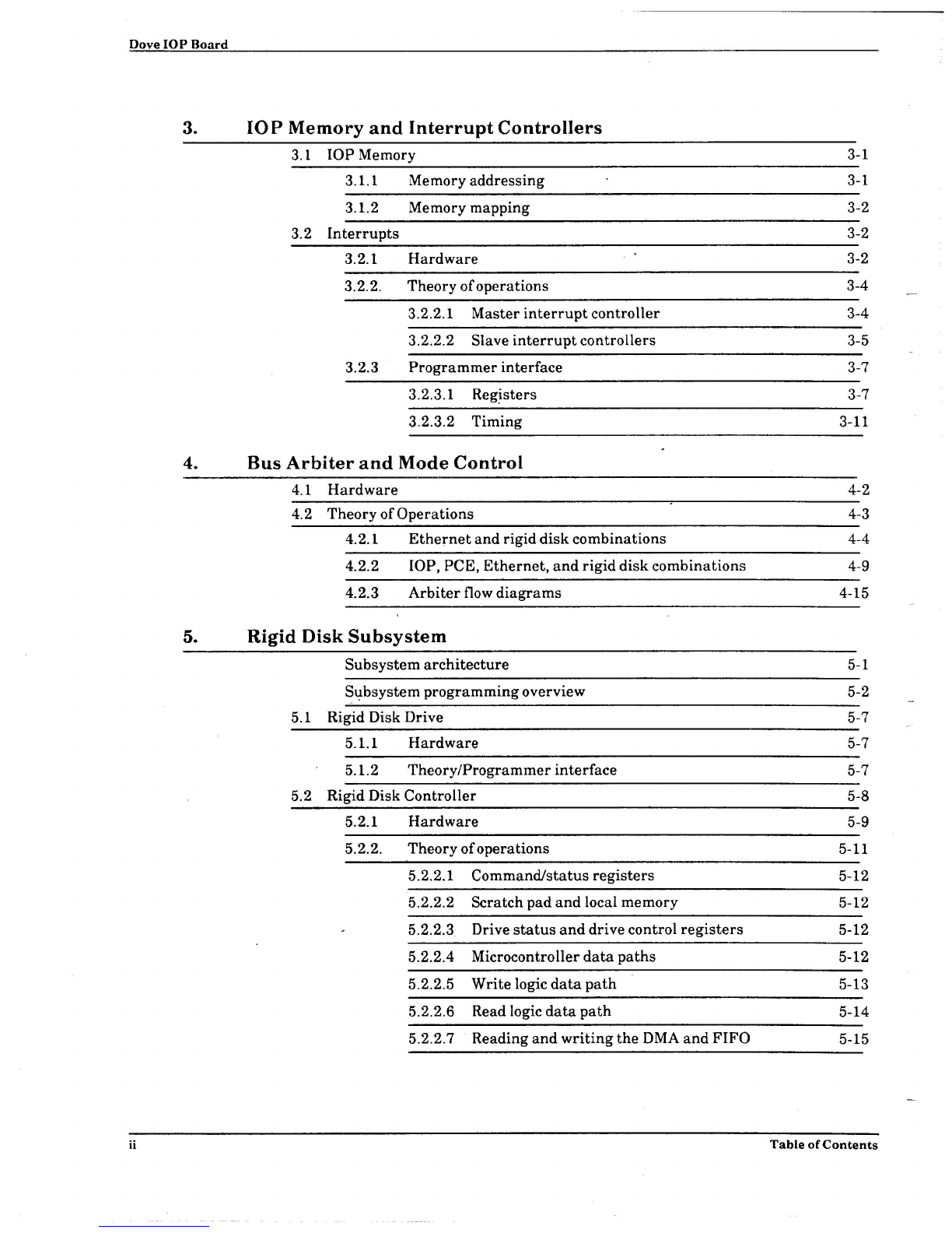
3.
lOP
Memory
and
Interrupt
Controllers
3.1
lOP
Memory
3.l.1
Memory
addressing
3.l.2
Memory
mapping
3.2
Interrupts
3.2.1
Hardware
3.2.2. Theory
of
operations
3.2.2.1
Master
interrupt
controller
3.2.2.2 Slave
interrupt
controllers
3.2.3
Programmer
interface
3.2.3.1
Reg~sters
3.2.3.2
Timing
4.
Bus
Arbiter
and
Mode
Control
4.1
Hardware
4.2
Theory
of
Operations
4.2.1
Ethernet
and
rigid
disk
combinations
4.2.2 lOP, PCE,
Ethernet,
and
rigid
disk
combinations
4.2.3
Arbiter
flow
diagrams
5.
Rigid
Disk
Subsystem
Subsystem
architecture
S~bsystem
programming
overview
5.1 Rigid Disk Drive
5.l.1
Hardware
5.l.2
Theory/Programmer
interface
5.2 Rigid Disk
Controller
5.2.1
Hardware
5.2.2.
Theory
of
operations
5.2.2.1
Command/status
registers
5.2.2.2
Scratch
pad
and
local
memory
5.2.2.3 Drive
status
and
drive
control
registers
5.2.2.4 Microcontroller
data
paths
5.2.2.5
Write
logic
data
path
5.2.2.6 Read logic
data
path
5.2.2.7 Reading
and
writing
the
DMA
and
FIFO
ii
3-1
3-1
3-2
3-2
3-2
3-4
3-4
3-5
3-7
3-7
3-11
4-2
4-3
4-4
4-9
4-15
5-1
5-2
5-7
5-7
5-7
5-8
5-9
5-11
5-12
5-12
5-12
5-12
5-13
5-14
5-15
Table
of
Contents

Dove
lOP
Board
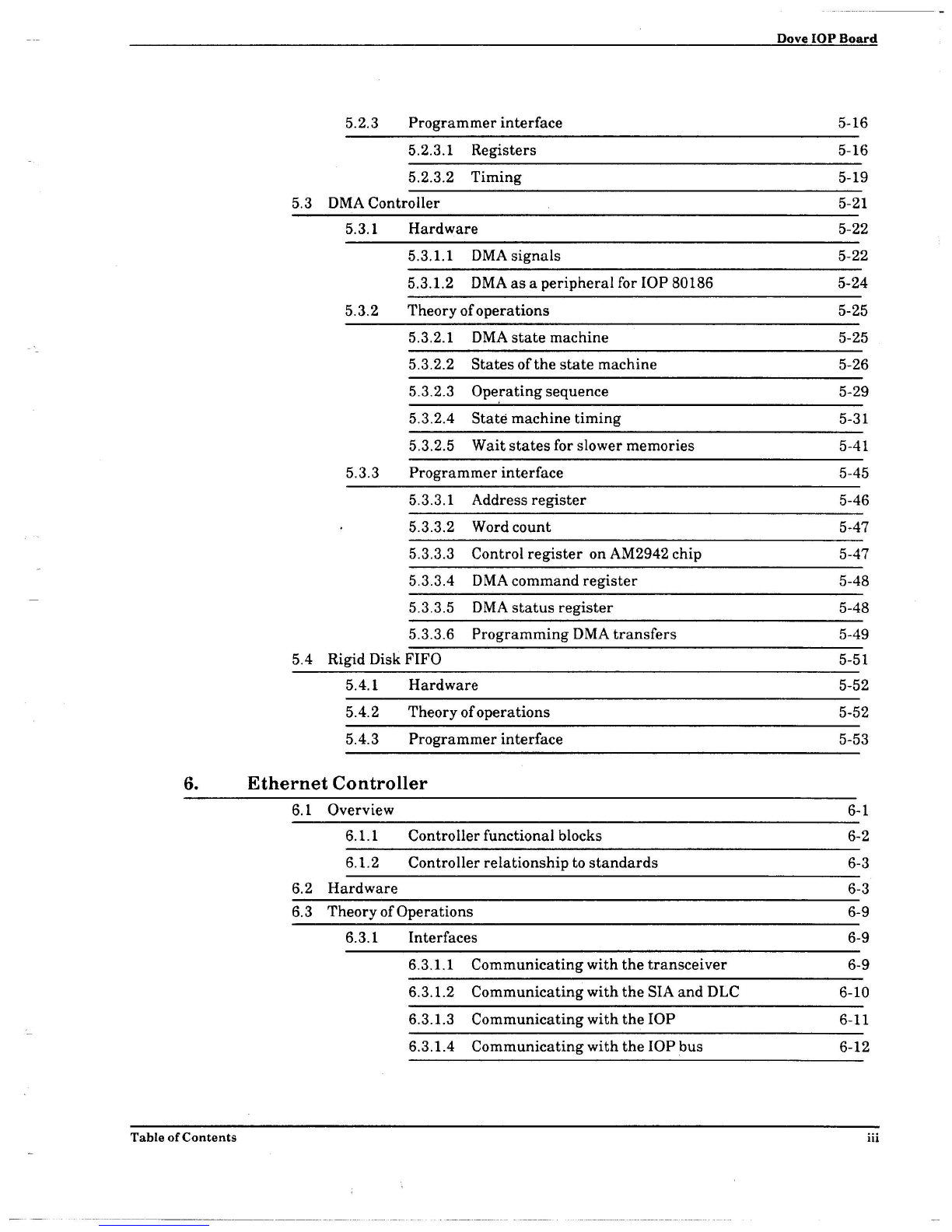
5.2.3
Programmer
interface
5-16
5.2.3.1
Registers
5-16
5.2.3.2
Timing
5-19
5.3 DMA
Controller
5-21
5.3.1
Hardware
5-22
5.3.1.1
DMA
signals
5-22
5.3.1.2 DMA
as
a
peripheral
for
lOP
80186 5-24
5.3.2
Theory
of
operations
5-25
5.3.2.1 DMA
state
machine
5-25
5.3.2.2
States
of
the
state
machine
5-26
5.3.2.3 Ope,rating
sequence
5-29
5.3.2.4
State
machine
timing
5-31
5.3.2.5
Wait
states
for
slower
memories
5-41
5.3.3
Programmer
interface
5-45
5.3.3.1 Address
register
5-46
5.3.3.2 Word
count
5-47
5.3.3.3 Control
register
on AM2942
chip
5-47
5.3.3.4 DMA
command
register
5-48
5.3.3.5 DMA
status
register
5-48
5.3.3.6
Programming
DMA
transfers
5-49
5.4 Rigid Disk
FIFO
5-51
5.4.1
Hardware
5-52
5.4.2
Theory
of
operations
5-52
5.4.3
Programmer
interface
5-53
6.
Ethernet
Controller
6.1
Overview
6-1
6.1.1
Controller
functional
blocks 6-2
6.1.2
Controller
relationship
to
standards
6-3
6.2
Hardware
6-3
6.3
Theory
of
Operations
6-9
6.3.1
Interfaces
6-9
6.3.1.1
Communicating
with
the
transceiver
6-9
6.3.1.2
Communicating
with
the
SIA
and
DLC 6-10
6.3.1.3
Communicating
with
the
lOP
6-11
6.3.1.4
Communicating
with
the
lOP
bus
6-12
Table
of
Contents
iii

Dove
lOP
Board
6.3.2 Processes
leading
to
data
transmission
and
reception
6-14
6.3.2.1
Initialization
6-14
6.3.2.2 Successful boot 6-15
6.3.3
Data
transmission
and
net
management
6-15
6.3.3.1
Transmission
6-16
6.3.3.2
Network
management
6-17
6.3.4
Data
reception 6-19
6.3.4.1
Initializing
6-19
6.3.4.2 Receiving a
frame
6-19
6.3.5 Diagnostics 6-21
6.3.5.1
Hardware
diagnostics 6-22
6.3.5.2 Software diagnostics 6-22
7.
Floppy
Disk
Subsystem
7.1
Hardware
7-2
7.1.1 Floppy
disk
drives
7-2
7.1.2
Diskettes
7-2
7.1.3 Floppy disk
controller
7-3
7.l.3.1
Controller
interface
7-3
7.1.3.2
Data
separator
7-6
7.2 Theory
of
Operations
7-8
7.2.1 Floppy
disk
controller
7-9
7.2.2
Data
separator
7-9
7.2.3 80186 processor (DMA
and
timer)
7-9
7.2.4
Interrupt
controllers
7-10
7.2.5 Control
register
7-10
7.2.6 Buses 7-10
7.3
Programmer
Interface 7-10
7.3.1 Registers 7-10
7.3.1.1 Floppy
disk
controller
registers
7-11
7.3.1.2 DMA
registers
7-13
7.3.1.3
Timer
registers
7-14
7.3.1.4
lOP
control
registers
7-14
7.3.2
Interrupts
7-16
7.3.3 Reset 7-16
7.3.4 Diskette
format
7-16
iv
Table
of
Contents

Dove
lOP
Board
7.3.4.1
Preambles
and
postambles 7-17
7.3.4.2 Sectors 7-18
8. RS232C
Controller
8.1
Hardware
8-1
8.1.1
Serial
controller
8-1
8.1.1.1
Controller
8-2
8.1.1.2
Timer
8-4
8.1.2 Interfaces 8-6
8.1.2.1
System
interface
signals
8-6
8.1.2.2 8274
interface
ports
8-7
8.1.2.3 Interface connectors 8-9
8.1.3
Serial
channels
8-10
8.2 Theory
of
Operations
8-11
8.3
Programmer
Interface: Registers 8-12
8.3.1
External
registers
8-12
8.3.2 8274
serial
controller
registers
8-13
8.3.2.1
Write
registers
8-13
8.3.2.2 Read
registers
8-17
8.3.3 8254
timer
registers
8-18
9.
Keyboard/Mouse
Controller
and
Maintenance
Panel
9.1
Hardware
9-1
9.2 Theory
of
Operations/Programmer
Interface
9-2
9.2.1 Keyboard
and
mouse
interface
9-2
9.2.2
Registers
9-3
9.2.2.1
Command
registers
9-3
9.2.2.2
Status
registers
9-5
9.2.3
Maintenance
panel
9-6
9.2.3.1
Normal
commands
9-7
9.2.3.2 Special
commands
9-7
10.
Debugger
Interface
10.1
Hardware
10-1
10.1.1
Interface
connector 10-3
10.1.2
Programmable
peripheral
interface
(PP[) 10-4
10.1.3 Line
drivers
10-4
Table
of
Contents
v

Dove
lOP
Board
Appendix
A
AppendixB
AppendixC
Appendix
0
vi
10
.1.4 Line receivers
10.2 Theory of
Operations
10.2.1 Sending and receiving
data
10.2.2
Handshaking
10.3
Programmer
Interface
10
.3.1 Addressing
the
debugger interface
10.3.2
Programming
the
PPI
10-5
10-5
10-5
10-6
10-7
10-7
10-7
10.3.2.1 Operational descriptions
and
configurations 10-7
10.3.2.2 Initialization 10-7
10.3.2.3
Sen~Hng
a byte 10-8
10.3.2.4 Receiving a byte 10-8
10.3.2.5 Sendingboot (Reset)
signal
to debuggee
machine
10-8
10.3.2.6 Sending
an
NMI
signal
10-9
10.3.3
Timing
10-9
Addendum:
Speaker
Appendices
Rigid
Disk
Subsystem
Supplemental
Information
Floppy
Disk
Controller
Command
Instruction
Set
Docu
men
tation
Representative
Schematics
for
the
lOP
Board
(separate
document)
Table
o(Contents

LIST OF FIGURES
Section
1 1.1 Dove
workstation
block
diagram
1-2
1.2 Loca
tions
of
PWBAs
on
the
backplane
1-3
1.3
lOP
board
layout
1-4
Section
2 2.1 I/O
subsystem
block
diagram
2-1
2.2 80186
chip
(top view)
2-2
2.3
80186
socket
pin
-
outs
(top view)
2-3
2.4 80186
pins
and
signals
2-4
2.5
80186 block
diagram
2-7
2.6 80186
registers
2-8
2.7
Integrated
DMA
unit
2-9
2.8
Timer
unit
block
diagram
2-9
2.9
Integrated
interrupt
controller
2-
10
2.
10
80186
integrated
peripheral
control
block
2-11
Section
3 3.1
lOP
address
space
3-1
3.2
lOP
memory
address
space
bit
assignment
3-2
3.3
IOP
interrupts
3-4
3.4
Interrupt
pointer
table
3-6
3.5
Content
of
first
interrupt
vector
byte
3-8
3.6
Content
of
second
interrupt
vector
byte
3-8
3.7
Content
of
third
interrupt
vector
byte
3-8
3.8
Content
of
interrupt
vector
byte
for
iAPX
86
system
mode 3-8
3.9
Initialization
command
word
format
3-9
3.10
Operation
command
word
format
3-10
3.
11
Interrupt
controller
INTA' cycle 3-11
Section
4 4.1
Arbitration
and
mode
control
block
diagram
4-1
4.
2-6
Arbiter
flow
diagrams
4-15
Table
oCContents
vii

Dove
lOP
Board
Section
5 5.1 Rigid disk subsystem 5-1
5.2
Data
transfer
path
between
main
memory
and
the
rigid
disk
5-3
5.3 Rigid
disk
format 5-7
5.4 8x305 microcontroller pin-out 5-9
5.5 Rigid
disk
controller block
diagram
5-11
5.6 RDC microcontroller
data
paths
5-13
5.7 RDC write logic
data
path
5-14
5.8 RDC
read
logic
data
path
5-15
5.9 RDC command
register
5-16
5.10 RDC
status
register
5-17
5.11 8x305
timing
5-19
5.12
Timing
for
read
data,
data
separator,
and
address
mark
detection 5-20
5.13
DMA
controller block
diagram
5-
21
5.14 Block
diagram
of
DMA
state
machine 5-25
5.15 DMA states: I -
Transfer
initiation
5-26
5.16
DMA
states
:
II
. Bus cycles 5-27
5.17
DMA
states: III.
Transfer
conclusion 5-28
5.18
DMA
timing
: No wait
states
5-32
5.19 DMA timing: One wait
state
5-33
5.20 DMA timing: Two wait
states
5-34
5.21
DMA
timing
:
Starting
DMA
operation
5-35
5.22 DMA timing:
Interrupt-
originated
Drop Disk Hold
request
5-36
5.23 DMA
timing
:
Continuing
DMA operation
after
suspension
5-37
5.24 DMA timing: FIFOOB Drop Disk Hold
request
5-38
5.25 DMA timing: FIFOOB
continuing
DMA
operation
5-39
5.26 DMA timing:
Ending
DMA
operation
5-40
5.27 IOPARDY timing:
Daybreak,
Alt
. I: One
wait
state
5-42
5.28 IOPARDY timing:
Daybreak,
Alt. II. One
wait
state
5-42
5.29 IOPARDY timing:
Daybreak,
Alt
I:
Five
wait
states
5-43
5.30 IOPARDY timing:
Daybreak,
Alt
II: Five
wait
states
5-43
5.31 IOPARDY timing: A chip: One
wait
state
5-44
5.32 IOPARDY timing: A chip:
Five
wait
states
5-44
5.33
Starting
address
register
5-46
viii
Table
of
Contents

Dove
lOP
Board
5.34 DMA
command
register
5-48
5.35 DMA
status
register
5-48
5.36
FIFO
block
diagram
5-51
5.37 Reset
timing
5-54
5.38
Asynchronous
read/write
timing
5-54
5.39
Full
flag
from
last
write
to
first
read
5-55
5.40
Empty
flag
from
last
read
to
first
write
5-55
Section
6 6.1
Ethernet
controller
block
diagram
6-2
6.2
Terminating
resistor
network
for
transceiver
cable
6-4
6.3
Ethernet
controller
and
interface
pins
and
signals
6-5
Section
7 7.1 Floppy
disk
subsystem
block
diagram
7-1
7.2
Diskettes
7-2
7.3 8272 floppy
disk
controller
pins
and
signals
7-4
7.4 8272 floppy
disk
controller
interface
pins
and
signals
7-5
7.5 9229
data
separator
pins
and
signals
7-7
7.6
System
interface
7-8
7.7 FDC
status
register
7-11
7.8
lOP
control
register
7-14
7.9 Floppy
disk
format
7-17
Section
8 8.1 RS232C block
diagram
8-1
8.2 8274
serial
controller
pins
and
signals
8-2
8.3 8254
timer
pins
and
signals
8-5
8.4
RS232C
system
interface
pins
and
signals
8-6
8.5 RS232C
channel
A DTE
port
8-8
8.6 RS232C
channel
B DCE
port
8-9
8.7 RS232C
controller
data
paths
8-11
8.8
Timing
for
8274
interrupt
acknowledge
8-12
Section
9 9.1 8251A
keyboard
controller
9-1
9.2 8251A
initialization
9-3
9.3
Command
register
during
mode
initialization
9-4
Table
of
Contents
ix

Dove
lOP
Board
9.4 Command
register
during
normal
operation 9-4
9.5
Status
register
9-5
Section
10 10.1 Debugger boards in a typical debugging
system
10-1
10.2 Debugger
interface
PWB
assembly
10-2
10.3 Debugger interface block
diagram
10-3
10.4 Intel PPJ pins
and
signals 10-4
10.5 Line
driver
circuits 10-4
10.6 Line receiver circuits 10-5
10.7 Flow
diagram
of
sending
and
receiving a byte 10-5
10.8
Transmission
cable flow 10-6
10.9
Timing
diagram
for
read
and
write 10-10
Addendum
Speaker
logic
Ad-l
Appendix
B
B.1
Command
phase
B-9
B.2 Execution
phase
(read
and
write instructions)
B-I0
B.3
Result
phase
(read
or
write instructions) B-11
B.4 Seek,
recalibrate,
sense
interrupt
status,
and
invalid
instructions
B-12
J[
Table
of
Contents

Dove
lOP
Board
LIST
OF
TABLES
Section
1 1.1
lOP
backplane
pin
assignment
(front
view) 1-6
1.2
lOP
expansion
channel
pin
assignment
1-7
Section
2 2.1 80186
pin
assignment
2-4
2.2 80186
initial
register
state
after
reset
2-12
2.3
lOP
110
controller
addresses:
PCSO, PCS1,
PCS4
2-14
2.4
Register
bit
maps
2-15
Section
3 3.1
Master
interrupt
controller
pin
description
3-3
3.2
Description
of
possible
interrupts
3-3
Section
4 4.1 Major
arbiter
logic
signals
4-2
4.2
Arbiter
flow sequence:
Ethernet
requests
service
4-4
4.3
Arbiter
flow sequence: RDC
requests
service
4-5
4.4 RDC
requests
service
then
Ethernet
requests
service
4-6
4.5 RDC
and
Ethernet
request
service
4-6
4.6 RDC
and
Ethernet
request
service
at
the
same
time
4-7
4.7
Ethernet
and
RDC
request
service
4-8
4.8
lOP
executes
AllowPCCmd' 4-9
4.9
lOP
requests
service
4-9
4.10
10P-~CE:
(PCE
executes
I/O Rd'
or
Wr') 4-10
4.11
lOP,
PCE,
and
RDC
request
service
4-11
4.12
lOP,
PCE,
and
Ethernet
request
service
4-12
4.13
lOP,
PCE,
RDC,
and
Ethernet
request
service
4-13
4.14
lOP,
PCE,
RDC
request
service
(interrupt
occurs) 4-14
Section
5 5.1 8x305
pin
description
5-10
5.2
Disk
commands
and
RDC
operations
5-16
5.3
Normal
register
sequence
5-18
5.4
Error
recovery
sequence
5-19
5.5 DMA
signal
description
5-23
Table
of
Contents
xi

Dove
lOP
Board
5.6 80186 bus control interface pin description 5-23
5.7 80186
data
bus
interface pin description 5-24
5.8 80186 DMA
program
signals
description 5-24
5.9
Data
transfer
operating
sequence 5-30
5.10 I/O
addresses
5-46
5.
11
Word count examples 5-47
Section
6 6.1
Data
link
controller
pin
assignments
6-6
6.2
Serial
interface
pin
assignments
6-8
6.3 DLC
error
reporting
capabilities
6-21
Section
7 7.1
Characteristics
of
formatted
diskettes
7-3
7.2 8272 pin
assignments
7-4
7.3 8272 interface pin
assignments
7-5
7.4 9229
pin
assignments
7-7
7.5 Registers
and
addresses 7-
11
7.6
DMA
registers
7-13
7.7
Timer
registers
7-14
Section
8 8.1 8274
serial
controller pin
assignments
8-2
8.2 Baud
rate
constants
8-4
8.3 8254
timer
pin
assignments
8-5
8.4
System
interface pin
assignments
8-7
8.5 Interface
signals
8-10
8.6
Serial
controller
registers
8-13
8.7
Write
register
0
(WRO)
8-14
8.8
Write
register
1 (WR1) 8-14
8.9
Write
register
2 (WR2):
Channel
A 8-15
8.
10
Write
register
2 (WR2):
Channel
B 8-15
8.11
Write
register
3 (WR3):
Channel
B 8-15
8.12
Write
register
4 (WR4) 8-16
8.13
Write
register
5 (WR5) 8-16
8.14
Write
register
6 (WR6) 8-16
8.15
Write
register
7 (WR7) 8-17
xii
Table
of
Contents

Dove
lOP
Board
8.16 Read
register
0
(RRO)
8-18
8.17 Read
register
1(RR1) 8-17
8.18 Read
register
2 (RR2)
8~18
8.19 8254
timer
read/write
operations
8-18
Section
9 9.1 8251A pins
and
signals 9-2
9.2 8257A
registers
9-3
9.3
Maintenance
panel code message 9-6
9.4
Command
instruction
set
9-8
Section
10 10.1 20-pin connector description 10-3
10.2
Handshaking
procedure 10-6
10.3 Basic
operations
of
the
debugger interface (PPI) 10-7
10.4 Configuration
of
the Intel 8255-A in
the
debugger
interface
10-8
10.5
Timing
characteristics
10-9
Appendix
A A.1 Disk
operations
A-I
A.2
Header
and
label
layout
in
scratch
pad
and
FIFO A-2
A.3
Error
codes A-5
A.4
States
of
the
state
machine: PROM
contents
A-8
Appendix
B B.1 Read
Data
instruction
set
B-2
B.2 Read Deleted
Data
instruction
set
B-2
B.3
Write
Data
instruction
set
B-3
B.4
Write
Deleted
Data
instruction
set
B-3
B.5 Read a
Track
instruction
set
B-4
B.6 Read ID
instruction
set
B-4
B.7
Format
a
Track
instruction
set
B-5
B.8 Scan
Equal
instruction
set
B-5
B.9
Scan
Low
or
Equal
instruction
set
B·6
B.10
Scan
High
or
Equal
instruction
set
B-7
B.11
Recalibrate
instruction
set
B-7
B.12 Sense
Interrupt
Status
instruction
set
B-7
B.13 Specify
instruction
set
B-8
Table
of
Contents
xiii

Dove
lOP
Board
B.14 Sense Drive
Status
instruction
set
B-8
B.
15
Seek
instruction
set B-8
B.16 Invalid
instruction
set
B-8
xiv Table
of
Contents