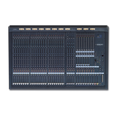
Yamaha CS1D User manual

SERVICE MANUAL
PA 011508
CONTENTS
REVISED PAGE LIST ··························································· 2-1
SPECIFICATIONS································································· 3-1
PANEL LAYOUT···································································· 3-3
CONNECTOR CIRCUIT DIAGRAM ········································· 4
DISASSEMBLY PROCEDURE··············································· 15
LSI PIN DESCRIPTION·························································· 31
IC BLOCK DIAGRAM ····························································· 39
CIRCUIT BOARDS································································· 45
INSPECTION·········································································· 98
TEST PROGRAM································································· 103
BLOCK DIAGRAM································································ 126
PARTS LIST
CIRCUIT DIAGRAM
CONTROL SURFACE
HAMAMATSU, JAPAN
Copyright (c) Yamaha Corporation. All rights reserved. PDF-K-**** '01.03

CS1D
2-1
REVISED PAGE LIST
<PARTS LIST>
SPECIFICATIONS
CONNECTOR CIRCUIT DIAGRAM
DISASSEMBLY PROCEDURE
LSI PIN DESCRIPTION
IC BLOCK DIAGRAM
CIRCUIT BOARDS
STO1,STO2,PS2HP
MTCPU
MB22
MIO
CIO
STI
AEI
CNDS2,PNIS4
CNDS1,LAMPVR,LCDC
PNC2,PNM4
ADA2
MO1-2,MO2-2
CNDS3,LCDIF
PCIF
PNIS3,PNM3
MTG,MTI
EIF
CCAS
ITEM
3-1
4,5,6,8,10
11,13,14,14a
18~23,25
32
39, 40
(45~97)
45
46, 47
48
49
50
51
52
53
54
55
56-a
56-b
57
58,59
60
61
64
65
PAGE
OVERALL ASSEMBLY
BOTTOM ASSEMBLY
PC ASSEMBLY
FRONT ASSEMBLY
SIDE PANEL (L,R) ASSEMBL
METER ASSEMBLY
LCD ASSEMBLY
ITEM
4,5
6,7,15~18
19
20
21
25
27
PAGE
CONTROL PANEL ASSEMBLY MASTER
PCMCIA ASSEMBLY
CONTROL PANEL ASSEMBLY OUT SEL
CONTROL PANEL ASSEMBLY IN SEL
CONTROL PANEL ASSEMBLY IN
ELECTRICAL PARTS
ITEM
28,30
31
32,33,34,35,36
37,38,39
40,41
42~103
PAGE
PNC1
CUTBVL2,HMVOLA2,HMVOLB2
DRL,DRN,DRS,PHNAB2
MT2
MT3
PNM1
PNOS4
MSCPU
PONOS2,PNOS5
PNOS3,PNOS6
PNOS1R
PNOS1L
PNOS1C
ISCPU
OSCPU
PNIS1
PNIS2
INCPU
PNI1
INSPECTION
TEST PROGRAM
BLOCK DIAGRAM
ITEM
66
68
69
70
71
72,73
75
76
78,79
80
81
82
83
86
88
90,91
92,93
94
96,97
98~102
103~125
126~154
PAGE

CS1D
2-2
<CIRCUIT DIAGRAM>
MB21 CIRCUIT DIAGRAM 002
MB22 CIRCUIT DIAGRAM
MIO CIRCUIT DIAGRAM 002
003
004
CIO1 CIRCUIT DIAGRAM 2/2
STI CIRCUIT DIAGRAM 2/2
AEI CIRCUIT DIAGRAM 005
STO1 CIRCUIT DIAGRAM
MO1-2 CIRCUIT DIAGRAM
MO2-2 CIRCUIT DIAGRAM
PNC1 CIRCUIT DIAGRAM 002
003
005
006
008
009
010
EIF,CCAS CIRCUIT DIAGRAM 002
003
006
007
008
CMU1 CIRCUIT DIAGRAM 003
004
005
006
008
009
CMU2 CIRCUIT DIAGRAM 003
005
006
007
MTG CIRCUIT DIAGRAM
MTCPU CIRCUIT DIAGRAM 002
003
004
006
007
008
009
CNDS1 CIRCUIT DIAGRAM
CNDS2 CIRCUIT DIAGRAM 1/3
2/3
ITEM
3
8
10
11
12
14
16
20
21
26
27
28
29
31
32
34
35
36
38
39
42
43
44
46
47
48
49
51
52
54
56
57
58
59
60
61
62
64
65
66
67
69
70
71
PAGE
CNDS3 CIRCUIT DIAGRAM
ADA2 CIRCUIT DIAGRAM 1/2
2/2
PNC2 CIRCUIT DIAGRAM 1/2
2/2
PCIF CIRCUIT DIAGRAM 002
003
004
005
006
007
008
PS2HP CIRCUIT DIAGRAM
MT1 CIRCUIT DIAGRAM 005
MT2,MT3 CIRCUIT DIAGRAM 006
LAMPVR CIRCUIT DIAGRAM
DRS,DRN,DRL CIRCUIT DIAGRAM
LCDIF CIRCUIT DIAGRAM
MSCPU CIRCUIT DIAGRAM 008
009
PNM1 CIRCUIT DIAGRAM 010
PNOS1L CIRCUIT DIAGRAM 009
PNOS1C CIRCUIT DIAGRAM 2/2
PNOS1R CIRCUIT DIAGRAM 004
PNOS2 CIRCUIT DIAGRAM 007
008
HMVOLA2, HMVOLB2 CIRCUIT DIAGRAM
TB1-2, TB1CAN2 CIRCUIT DIAGRAM
CUTBVL2 CIRCUIT DIAGRAM
OSCPU CIRCUIT DIAGRAM 005
010
CRDC1 CIRCUIT DIAGRAM 002
003
ISCPU CIRCUIT DIAGRAM 005
PNIS1 CIRCUIT DIAGRAM 005
008
PNIS2 CIRCUIT DIAGRAM 003
005
008
PHNAB2 CIRCUIT DIAGRAM
PNI1 CIRCUIT DIAGRAM 008
INCPU CIRCUIT DIAGRAM 006
PS2000 CONNECTOR DIAGRAM
ITEM
73
74
75
76
77
78
79
80
81
82
83
84
86
90
95
96
97
98
106
107
117
132
134
137
143
144
150
151
152
156
161
162
163
170
177
180
185
187
190
195
202
210
213, 214
PAGE

CS1D
2-3
WARNING: CHEMICAL CONTENT NOTICE!
The solder used in the production of this product contains LEAD. In addition, other electrical/electronic and/or plastic (where
applicable) components may also contain traces of chemicals found by the California Health and Welfare Agency (and possibly
other entities) to cause cancer and/or birth defects or other reproductive harm.
DO NOT PLACE SOLDER, ELECTRICAL/ELECTRONIC OR PLASTIC COMPONENTS IN YOUR MOUTH FOR ANY REASON
WHAT SO EVER!
Avoid prolonged, unprotected contact between solder and your skin! When soldering, do not inhale solder fumes or expose eyes
to solder/flux vapor!
If you come in contact with solder or components located inside the enclosure of this product, wash your hands before handling
food.
IMPORTANT NOTICE
This manual has been provided for the use of authorized Yamaha Retailers and their service personnel. It has been assumed that
basic service procedures inherent to the industry, and more specifically Yamaha Products, are already known and understood by
the users, and have therefore not been restated.
WARNING: Failure to follow appropriate service and safety procedures when servicing this product may result in personal
injury, destruction of expensive components and failure of the product to perform as specified. For these
reasons, we advise all Yamaha product owners that all service required should be performed by an authorized
Yamaha Retailer or the appointed service representative.
IMPORTANT: This presentation or sale of this manual to any individual or firm does not constitute authorization, certification,
recognition of any applicable technical capabilities, or establish a principal-agent relationship of any form.
The data provided is belived to be accurate and applicable to the unit(s) indicated on the cover. The research engineering, and
service departments of Yamaha are continually striving to improve Yamaha products. Modifications are, therefore, inevitable and
changes in specification are subject to change without notice or obligation to retrofit. Should any discrepancy appear to exist,
please contact the distributor's Service Division.
WARNING: Static discharges can destroy expensive components. Discharge any static electricity your body may have
accumulated by grounding yourself to the ground bus in the unit (heavy gauge black wires connect to this bus).
IMPORTANT: Turn the unit OFF during disassembly and parts replacement. Recheck all work before you apply power to the
unit.
WARNING
Components having special characteristics are marked and must be replaced with parts having specification equal to those
originally installed.
LITHIUM BATTERY HANDLING
This product uses a lithium battery for memory back-up.
WARNING: Lithium batteries are dangerous because they can be exploded by improper handling. Observe the following
precautions when handling or replacing lithium batteries.
Leave lithium battery replacement to qualified service personnel.
Always replace with batteries of the same type.
When installing on the PC board by soldering, solder using the connection terminals provided on the battery cells.
Never solder directly to the cells. Perform the soldering as quickly as possible.
Never reverse the battery polarities when installing.
Do not short the batteries.
Do not attempt to recharge these batteries.
Do not disassemble the batteries.
Never heat batteries or throw them into fire.
ADVARSEL!
Lithiumbatteri-Eksplosionsfare ved fejlagtig håndtering. Udskiftning må kun ske med batteri af samme fabrikat og type. Levér det
brugte batteri tilbage til leverandøren.
VARNING
Explosionsfara vid felaktigt batteribyte.
Använd samma batterityp eller en ekvivalent typ som rekommenderas av apparattillverkaren.
Kassera använt batteri enligt fabrikantens instruktion.
VAROITUS
Paristo voi räjähtää, jos se on virheellisesti asennettu.
Vaihda paristo ainoastaan laitevalmistajan suosittelemaan tyyppiin.
Hävitä käytetty paristo valmistajan ohjeiden mukaisesti.
The following information complies with Dutch Official Gazette 1995. 45; ESSENTIALS OF ORDER ON THE COLLECTION OF
BATTERIES.
• Please refer to the diassembly procedure for the removal of Back-up Battery.
• Leest u voor het verwijderen van de backup batterij deze beschrijving.

CS1D
3-1
SPECIFICATIONS
IMPORTANT NOTICE FOR THE UNITED KINGDOM
Connecting the Plug and Cord
IMPORTANT. The wires in this main lead are coloured in
accordance with the following code:
BLUE: NEUTRAL
BROWN: LIVE
As the colours of the wires in the main lead of this apparatus may not
correspond with the coloured markings identifying the terminals in
your plug, proceed as follows:
The BLUE wire must be connected to the terminal that is marked with
the letter N (or coloured BLACK).
The BROWN wire must be connected to the terminal that is marked
with the letter L (or coloured RED).
Be certain that neither core is connected to the earth terminal of the
three pin plug.
Number of scene memories 990
Sampling Frequency Intermal:48 kHz/44.1 kHz
External: 44.1 kHz -10 %–48 kHz +6 %
Fader 64 x 100 mm motorized
Total Harmonic Less than 0.02 % 20 Hz–20 kHz @
+24 dB into 600 Ω
Distortion Less than 0.007 % 1kHz @ +24 dB
into 600 Ω
CH IN to STEREO OUT
AD converter 28 bit 128 times over sampling
(Signal Delay 1.5 msec @ Fs=48 kHz)
DA converter 27 bit 128 times over sampling
(Signal Delay 1.2 msec @ Fs=48 kHZ)
Frequency Response +1, -2 db 20 Hz–20 kHz @ +10 db
into 600 Ω
Dynamic Range 120 dB typ. AD+DA (“LMY-” AD card
(maximum level to noise level) to DA card)
Hum & Noise -128 dB typ. Equivalent Input Noise.
(Rs=150 W) (20 Hz–20 kHz)
(Input Gain=Max.)
InputSection CH1–96, ST IN1–8
De-emphasis/DC cut
Phase Normal/Reverse
Patch Input, Direct out
(pre eq/pre fader/post fader/post on),
Insert in/out (pre eq/post eq/pre
comp/pre delay/pre fader)
Attenuation -96–0 dB ( dB step)
High pass filter 20 Hz–600 Hz (60 point) slope -6 dB /
-12 dB / -18 dB/oct
Equalizer 4 band PEQ
(Low/shelving, Low-mid, High-mid,
High/Shelving/LPF)
F: 20 Hz–20 kHZ (120 point),
Gain: + -18 dB (0.5 step),
Q: 0.1–10 (41 point)
Gate Gate/Ducking selectable 4 key-n bus
Comp Comp/Expander/compander
selectable 4 key-in bus
Delay Delay time (0–250 ms, 0.02 msec step)
Fader 100 mm motorized, -∞, -90– +10 dB
(128 step/100 mm),
Interpolation 24bit (16,777,216 steps)
On/Off
Cue/Solo On/Off (PFL/AFL)
Pna 127 positions (L=1–63, center, R=1–63)
Stereo/group assign STEREO/MIX 1–48 (FIX/VARI
selectable)
Metering pre att peak, comp/gate gain reduction,
pre att/pre gate/pre fader/post fader/
post on selectable with Peak-Hold
Output section STEREO A, B, MIX 1–48, MATRIX 1–24
Patch Output, Insert in/out
Equalizer 6 band PEQ
(Sub Low/HPF/Shelving, Low, Low-mid,
Mid, High-mid, High/LPF/Shelving)
(Bypass switch for each band)
(Parameters are same as input EQ)
Comp Comp/Expander/compander selectable,
4 key-in bus
Delay Delay time (0–1000 ms, 0.02 msec step)
On/Off
Cue/Solo On/Off (PFL/AFL)
Balance Stereo A, B, Paired Mix & Matrix
Mono Stereo B
to stereo assign from Mix output
to matrix assign from Mix 1–48/stereo A, B
Metering comp gain reduction, pre eq/pre fader/post
fader/ post on selectable with Peak-Hold
Dither On/Off, Word length 16–24 bit (DIO8 only)
Other mixer section
Effects Internal patchable eight multi-effects
units
Graphic equalizer Internal patchable twenty four 31-
band graphic equalizers, each with 4
notch filters
Oscillator sine/pink/burst noise
Talk back From console 1 & 2
Communication In Including ducking control
12 DCA with DCA mute, DCA cue/solo, 9–12
are selectable for output
12 Direct Memory Recall/Mute Group
Monitor A 2tr in 1, 2, ST A, B, user define
selectable with delay (max 750 msec)
Monitor B 2tr in 1, 2, ST A, B, moni A, user
define selectable
2tr in 1–6 1 & 2: Analog/Coaxial/AES/EBU
selectable,
3–6: AES/EBU
(with Sampling Rate Converter for
digital input)

CS1D
3-2
ANALOG INPUT CHARACTERISTICS
Input
Terminals GAIN Actual Load
Impedance For Use With
Nominal Input level
Nominal Max. before clip Connector
TALKBACK IN
1, 2 *3. *5.
2-TRACK IN
ANALOG 1, 2 *4.
-44 dB
+10 dB
–
3 kΩ
10 kΩ
50–600 ΩMics &
600 ΩLines
600 ΩLines
XLR-3-31 type
(Balanced) *1.
XLR-3-31 type
(Balanced) *1.
-44 dB (4.89 mV) -30 dB (24.5 mV)
+10 dM (2.45 V) +24 dB (12.3 V)
+10 dB (2.45 V) +24 dB (12.3 V)
*1. TALKBACK IN and 2-TRACK IN ANALOG XLR-3-31 type connectors are balanced. (1=GND, 2=HOT, 3=COLD)
*2. 0 dB is referenced to 0.775 Vrms.
*3. AD converters are 24 bit linear, 128 times oversampling.
*4. AD converters are 28 bit 128 times oversampling.
*5. +48 V DC (Phantom power) is individuakky supplied to each TALKBACK connectors via 6.8 k ohms resistors.
ANALOG OUTPUT CHARACTERISTICS
Input
Terminals Actual Load
Impedance For Use With
Nominal Input level
Nominal Max. before clip Connector
MONITOR OUT A, B
CUE OUT
PHONES A1, B1
PHONES A2, B2
150 Ω
150 Ω
15 Ω
15 Ω
600 ΩLines
600 ΩLines
8 ΩPhones
40 ΩPhones
8 ΩPhones
40 ΩPhones
XLR-3-32 type
(Balanced) *1.
XLR-3-32 type
(Balanced) *1.
Stereo Phone Jack
(Unbalanced) *2.
Stereo Phone Jack
(Unbalanced) *2.
+10 dB (2.45 V) +24 dB (12.3 V)
+10 dM (2.45 V) +24 dB (12.3 V)
75 mW 150 mW
65 mW 150 mW
75 mW 150 mW
65 mW 150 mW
DIGITAL INPUT&OUTPUT CHARACTERISTICS
INPUT/OUTPUT
TERMINALS FORMAT LEVEL CONNECTOR
TYPE QUANTITY
DIGITAL I/O
ENGINE A1, A2
ENGINE B1, B2
CONSOLE 1, 2
2-TRACK IN DIGITAL
AES/EBU 1–6
2-TRACK IN DIGITAL
COAXIAL 1–2
STEREO OUT DIGITAL
AES/EBU A, B
STEREO OUT DIGITAL
COAXIAL A, B
WORD CLOCK IN
WORD CLOCK OUT
SVGA OUT
KEYBOARD
MOUSE
NUMKEY
REMOTE RS-422
MIDI IN, OUT, THRU
TIME CODE IN
GPI
PC CONTROL USB
PC CONTROL RS-232-C
–
AES/EBU
IEC60958
AES/EBU
IEC60958
–
–
SVGA
PS2
PS2
PS2
–
MIDI
SMPTE
–
–
–
RS422
RS422
0.5 Vpp/75 Ω
RS422
0.5 Vpp/75 Ω
TTL/75 Ω(ON/OFF)
TTL/75 Ω
2 Vpp
TTL
TTL
TTL
RS422
–
Nominal-10 dB/10 kΩ
C-MOS IN,
Open collector out
0 V–3.3 V
RS-232-C
D-SUB Half Pitch Connector 68P 6
(Female)
XLR-3-31 type Connector 6
PIN JACK 2
XLR-3-32 type Connector 2
PIN JACK 2
BNC Connector 1
BNC Connector 1
High density D-sub 15pin Connector (Female) 1
Mini DIN 6pin Connector 2
Mini DIN 6pin Connector 1
D-sub 9pin Connector (Female) 1
DIN 5pin Connector 3
XLR-3-31 type Connector 1
D-SUB 25pin Connector (Female) 1
B Type USB Connector 1
D-SUB 9pin Connector (Male) 1
*1. MONITOR OUT and CUE OUT XLR-3-32 type connectors are balanced. (1=GND, 2=HOT, 3=COLD)
*2. PHONES stereo phone jack are unbalanced. (Tip=LEFT, Ring=RIGHT Sleeve=GND)
*3. 0 dB is referenced to 0.775 Vrms.
*4. DA converters are 24 bit linear, 128 times oversampling.

CS1D
3-3
PANEL LAYOUT
Note: See operation manual for details.
INPUT/OUTPUT
TERMINALS FORMAT LEVEL CONNECTOR
TYPE QUANTITY
CONTROL I/O
ENGINE A1IN, 1OUT, 2IN, 2OUT
ENGINE B1IN, 1OUT, 2IN, 2OUT
CONSOLE 1IN, 1OUT, 2IN, 2OUT
DC POWER INPUT
–
–
-0.225 V–-1.825 V
DC 60 V
BNC Connector 68P 12
KN-27-32S 27pin Connector (Female) 2
LCD Display 800 x 600 Dots Graphic color LCD with backlit
PCMCIA card slot for external memory
PW1D Power Supply to the CS1D

KEC-92541-2 7
6P
PNI1(CN803)
6P
CNDS1(CN101)
16P
16P
CNDS1(CN105)
CNDS1(CN106)
6P
CNDS1(CN102)
16P
16P
CNDS1(CN107)
CNDS1(CN108)
6P
16P
16P
6P
CNDS3(CN503)
16P
16P
CNDS3(CN507)
CNDS3(CN508)
INCPU(CN4)
INCPU(CN5)
INCPU(CN1)
12P
12P
PNC2(CN104)
16P
16P
12P
12P
PNC2(CN106)
12P
PNC2(CN103)
6P
CNDS3(CN504)
16P
16P
CNDS3(CN509)
CNDS3(CN510)
12P
PNC2(CN105)
PNI1(CN803)
INCPU(CN4)
INCPU(CN5)
INCPU(CN1)
6P
PNI1(CN803)
INCPU(CN4)
INCPU(CN5)
INCPU(CN1)
12P
16P
16P
6P
PNI1(CN803)
INCPU(CN4)
INCPU(CN5)
INCPU(CN1)
12P
16P
16P
6P
7P
5P
CNDS2(CN205)
CNDS2(CN206)
CNDS2(CN318)
6P
7P
5P
ISCPU(CN5)
PHNAB2(CN301)
ISCPU(CN11)
ASSY CONTROL PANEL IN
ASSY CONTROL PANEL INSEL
6P
4P
10P
10P
MSCPU(CN44)
PNM1(CN957)
MSCPU(CN31)
ASSY CONTROL PANEL MAS
6P
4P
10P
10P
PNM1(CN956)
CNDS2(CN306)
CNDS2(CN303)
CNDS2(CN302)
PNC2(CN110)
6P
7P
6P
OSCPU(CN37)
ASSY CONTROL PANEL OUTSEL
TB1-2(CN701)
OSCPU(CN18)
6P
7P
6P
CNDS2(CN310)
CNDS2(CN309)
CNDS2(CN315)
3P
OSCPU(CN17)
HMVOLB2(CN203)
10P
10P
PNC2(CN108)
ADA2(CN104)
ADA2(CN300)
ADA2(CN105)
3P
HMVOLA2(CN103)
6P
HMVOLA2(CN100)
6P
HMVOLB2(CN200)
3P
HMVOLB2(CN206)
3P
HMVOLB2(CN205)
6P
CUTBVL2(CN500)
3P
CUTBVL2(CN503)
3P
6P
6P
3P
3P
PHNAB2(CN300)
ADA2(CN307)
MO1-2(CN402)
3P
CUTBVL2(CN504)
3P
3P
MO2-2(CN605)
ADA2(CN306)
ADA2(CN304)
ADA2(CN107)
ADA2(CN108)
80P
40P
80P
40P
CRDC1(CN101)
CRDC1(CN105)
PCIF(CN201)
PCIF(CN202)
6P
8P
6P
8P
PS2HP(CN601) PCIF(CN305)
ADA2(CN302)
FRONT ASSY
PS2HP(CN602)
3P
HMVOLA2(CN104)
3P
ADA2(CN308)
METER ASSY
2P
4P
4P
LAMPVR(CN701) CNDS2(CN200)
DRL(3)(CN100)
DRL(2)S(CN100)
DRS(CN100)
CNDS2(CN201)
12P
12P
12P
12P
12P
MT1(CN4)
MT2(CN5)
MT3(CN5)
12P
12P
12P
MT1(CN2)
8P
MT2(CN2)
9P
MT2(CN1)
14P
12P
12P
12P
8P
9P
14P
CNDS2(CN202)
CNDS2(CN204)
CNDS2(CN207)
MTCPU(CN7)
MTCPU(CN6)
MTCPU(CN5)
4P
5P
LCD-BACKLIGHT(CN1) CNDS2(CN301)
PCIF(CN304)
LCD ASSY
LCDIF(CN303)
PCIF(CN303)
LCDIF(CN302)
LCDIF(CN301) PCIF(CN302)
3P
2P
9P
10P
27P
CN28
CN29
CN24
CN20
FG
3P
2P
9P
10P
27P
CN26
CN27
CN25
CN21
FG
[1/49] – [12/60]
[13/61] – [24/72] [37/48] – [85/96]
[25/73] – [36/84]
ASSY CONTROL PANEL IN ASSY CONTROL PANEL IN
ASSY CONTROL PANEL IN
BOTTOM ASSY
ISCPU(CN3)
PNC2(CN107)
10P
10P
14P
14P
12P 12P
15P
15P
**
**
**
**
**
**
[DC POWER INPUT A] [DC POWER INPUT B]
DRL(1)(CN100)
DRN(CN100)
PCIF(CN306)
TPSW(CN101)
3P
TB1-2(CN702)
3P
HMVOLB2(CN204)
8P
8P
8P
8P
6P
MO1-2(CN403)
3P
ADA2(CN305)
6P
ADA2(CN106)
6P
TB1-2(CN703)
3P
HMVOLA2(CN106)
3P
HMVOLA2(CN105)
PHNAB2(CN305)
3P
PHNAB2(CN304)
3P
PHNAB2(CN303)
3P
PHNAB2(CN302)
3P
4P
4P
CS1D
4
CONNECTOR CIRCUIT DIAGRAM

2P
2P
4P
CN18
CN12
CN13
6P
2P
CN10
CN14
6P
CN11
2P
CN15
6P
CN2
6P
CN3
6P
6P
13P
CN100
CN103
CN104
6P
6P
16P
16P
16P
16P
CN101
CN102
CN105
CN106
CN107
CN108
50P 40P 40P 40P
CN1
CN6
CN5
CN4
100P 100P 100P 100P 100P 100P 100P 100P 100P
5P
5P
CN101
CN2
CN1
CN1CN200CN100 CN2 CN2
CN100CN100CN100
[ENGINE A]
[1]
[2]
[ENGINE B]
[1]
[2]
[CONSOLE]
[1]
[2]
[DIGITAL I/O]
[AES/EBU]
[1]
[2] [COAXIAL]
[AES/EBU]
[3]
[4]
[5]
[6]
[1]
[2]
[75 ]
[IN]
[OUT] [WORD CLOCK]
[ON]
[OFF]
[STEREO OUT]
[DIGITAL]
[2TR IN DIGITAL]
CN15 CN14 CN13 CN12 CN11 CN10 CN9 CN8 CN7
[AES/EBU]
[COAXIAL]
[AES/EBU]
[AES/EBU]
[AES/EBU]
[AES/EBU]
[COAXIAL]
[AES/EBU]
[COAXIAL]
CN201
13P
3P
3P
3P
2P
30P
50P 40P 40P 40P
CN11
CN14
CN12
CN10
CN13
CN4
CN15
CN16
15P
CN8
CN3
10P
CN1
14P
9P
8P
CN7
CN6
CN5
to ADA2(CN303) See P.4
to PNC2(CN109) See P.5
to MO1-2(CN400) See P.4
to MO1-2(CN405) See P.4
to MO2-2(CN602) See P.4
to MO2-2(CN604) See P.4
to MB22(CN503) See P.4
**
from POWER UNIT(CN5,6)
from POWER UNIT(CN11,12)
from POWER UNIT(CN13,14)
from POWER UNIT(CN34,35)
from POWER UNIT(CN37,38)
from POWER UNIT(CN22)
from POWER UNIT(CN23)
• BOTTOM ASSY (UNDER THE LEFT-SIDE ASSY CONTROL PANEL IN)
**
**
**
**
MTCPU
MIO
MIO
MIO
MIO
MIO
CIO
STI
AEI
STO1
STO2
MB21
CNDS1
KEC-92541-3 7
CS1D
5

CS1D
6
to CNDS3(CN65)
6P
6P
CN31
CN34
6P
CN30
6P
CN35
8P
CN41
6P
2P
CN39
CN32
4P CN38
2P
4P
4P
CN36
CN40
CN37
2P
CN33
CN204
CN207
4P
CN201
CN202
2P
CN200
12P
12P
12P
4P
CN301
to CNDS3(CN60)
**
• BOTTOM ASSY(UNDER THE ASSY CONTROL PANEL MAS/OUTSEL/INSEL)
4P
CN13
6P
6P
4P
CN5
CN6
CN11
2P
CN23
2P
6P
CN7
6P
CN19
4P
CN36
4P
CN39
2P
4P
CN17
4P
CN18
3P
2P
9P
10P
27P
CN28
CN29
CN24
CN20
FG
4P
CN12
4P
CN14
9P
CN34
9P
CN35
3P
3P
CN37
CN38
6P
6P
6P
CN8
CN9
CN10
CN22
3P
2P
9P
10P
27P
CN26
CN27
CN25
CN21
FG
4P
4P
CN15
CN16
CN40
POWER UNIT
**
**
**
**
**
**
**
**
to CNDS1(CN14)
to CNDS1(CN11)
to CNDS1(CN15)
to CNDS1(CN18)
to CNDS1(CN10)
to CNDS1(CN13)
to CNDS1(CN12)
to CNDS3(CN68)
to CNDS3(CN67)
to CNDS3(CN66)
to CNDS3(CN61)
to CNDS3(CN62)
from MTCPU(CN13)
from MTCPU(CN4)
from MTCPU(CN15)
from MTCPU(CN16)
from MTCPU(CN8)
from MTCPU(CN3)
CN501
CN503
10P
30P
100P
CN502 [2-TRACK IN]
[ANALOG]
[1]
[2]
[L]
[R]
[L]
[R]
CN500
MB22 LMY4AD AD2
CNDS2
KEC-92541-4 7
7P
6P
8P
5P
CN205
CN206
CN203
CN312
CN318
CN601
CN602
3P
6P
CN402
CN401
10P
4P
6P
10P
CN306
CN303
CN302
8P
CN101
CN201
CN202
CN801
CN802
80P 40P
20P50P
8P
CN300
7P
6P
CN310
CN309
5P
CN301
8P
8P
6P
CN300
CN103
8P
6P
3P
3P
3P
2P
6P
CN315
5P
8P
6P
CN319
CN317
CN316
CN101
CN102
8P
CN104
CN105
10P
CN303
CN306
CN100
CN307
CN604
6P
CN605
6P
CN403
8P
3P
CN302
CN308
CN302
6P
CN303
CN304
CN305
15P
14P
12P
3P
3P
CN304
CN305
**
[A]
[B]
[L]
[R]
[L]
[R] [MONITOR OUT]
[ANALOG]
[TALKBACK IN 2]
[CUE OUT ANALOG]
[L]
[R]
[SVGA OUT]
[KEY BOARD]
[MOUSE]
[NUM KEY]
[REMOTE] [RS-422]
from MB23(CN109)
from MB23(CN108)
CPU CARD
240P
**
CN102
8P
CN306
6P
CN106
3P
CN107
3P
CN108
10P
6P
CN606
8P
CN404
CN400
8P
CN406
8P
CN603
3P
CN405
11P
CN600
11P
15P
**
**
PCIF
ADA2
MO2-2
MO1-2

CS1D
7
6P
2P
CN60
CN68
8P
4P
4P
CN67
CN62
2P
6P
CN61
CN65
CN66
4P
4P
4P
6P
CN501
CN502
CN506
CN505
4P
4P
4P
6P
5P
5P
CN507
CN508
CN500
6P
CN503
CN509
CN510
6P
CN504
16P
16P
16P
16P
CN110
CN111
CN114
CN113
CN101
CN101
40P
CN102
40P
CN103
CN104
CN105
CN106
CN107
CN108
CN109
CN110
10P
10P
10P
10P
12P
12P
12P
12P
CN108
CN109
20P
50P
96P
CN101CN101 CN101 CN101CN101
CN104
CN101
96P
96P
96P
96P
96P
10P 12P
12P
10P
CN105
CN201
CN202
[IN]
[OUT]
[THRU] [MIDI]
[TIME CODE IN]
[GPI]
[USB]
[RS-232-C] [PC CONTROL]
[1]
[2]
[IN] [OUT]
[IN] [OUT] [ENGINE A]
[1]
[2] [IN] [OUT]
[IN] [OUT] [ENGINE B]
[1]
[2] [IN] [OUT]
[IN] [OUT] [CONSOLE]
[CONTROL I/O]
CN107 CN106 CN105 CN104 CN103 CN102
from POWER UNIT(CN5,6)
from POWER UNIT(CN11,12)
from POWER UNIT(CN13,14)
from POWER UNIT(CN19)
from POWER UNIT(CN34,35)
from POWER UNIT(CN37,38)
to PCIF(CN801)
from MTCPU(CN1)
to PCIF(CN802)
from POWER UNIT(CN17,18)
• BOTTOM ASSY(UNDER THE RIGHT-SIDE ASSY CONTROL PANEL IN)
**
**
**
**
**
**
**
CNDS3
PNC2
PNC1
CCAS
CMU1
CMU2
MB23
EIF
EIF
MTG
KEC-94541-5

CS1D
8
• FRONT ASSY
6P
8P
CN601
CN602
• METER ASSY
CN4
9P
CN1
CN5
12P
8P
CN6
9P
CN5
9P
CN4
CN3
12P
8P
CN3
CN5
9P
8P
CN1
CN2
12P
14P
9P
CN2
CN2
CN1
• LCD ASSY
2P
CN401
3P
5P
CN301
CN302
CN303
12P
14P
15P
LCD
41P
3P
CN304
CN3
CN1 CN2
10P
10P
[MOUSE]
[KEYBOARD]
[MONITOR A]
[MONITOR B]
LCD-
BACKLIGHT
**
**
PS2HP
MT1
MT2
MT3
LCDIF
LCDC
KEC-92541-6
4P
4P
CN701
CN100
2P
2P
CN101 CN102
12P
NC
**
[LAMP]
[LAMP]
[LAMP]
[LAMP]
4P
CN100
2P
2P
12P
FAN
CN100
2P
2P
12P
4P
CN100
2P
2P
12P
FAN
4P
CN100
2P
2P
12P
[LAMP DIMMER]
**
**
**
**
[FAN]
[HIGH]
[LOW]
LAMPVR
DRL (3)
DRL
DRS
(2)
DRL (1)
DRN
CN101 CN102
CN101 CN102
CN101 CN102
CN101 CN102
5

CS1D
9
• ASSY CONTROL PANEL MAS
4P
FADER
2P
7P
CN100
CN953
CN954
CN950
CN955
40P
40P
40P
20P
4P
3P
7P
CN16
CN32
CN1
4P
3P
7P
CN17
CN33
CN2
4P
3P
7P
CN18
CN34
CN3
4P
3P
7P
CN19
CN35
CN4
4P
3P
7P
CN20
CN36
CN5
4P
3P
7P
CN21
CN37
CN6
4P
3P
7P
CN22
CN38
CN7
4P
3P
7P
CN23
CN39
CN8
40P
40P
40P
20P
CN15
CN28
CN14
CN13
5P
CN501
5P
CN501
8P
CN400
4P
3P
7P
CN24
CN40
CN9
4P
3P
7P
CN25
CN41
CN10
4P
3P
7P
CN26
CN42
CN11
4P
3P
7P
CN27
CN43
CN12
5P
5P
CN46
CN29
8P
CN30
6P
4P
CN957
CN956
CN44
10P
CN31
10P
[1]
[2]
[3]
[4]
[5]
[6]
[7]
[8]
[9]
[10]
[11]
[12]
**
**
**
**
**
**
**
**
**
**
**
**
VR MT
MSCPU
PNM2
4P
FADER
2P
7P
CN100 VR MT
PNM2
4P
FADER
2P
7P
CN100 VR MT
PNM2
FADER
7P
CN100 VR MT
PNM2
PNM1
4P 2P
FADER
7P
CN100 VR MT
PNM2
4P 2P
FADER
7P
CN100 VR MT
PNM2
4P 2P
FADER
7P
CN100 VR MT
PNM2
4P 2P
FADER
7P
CN100 VR MT
PNM2
4P 2P
FADER
7P
CN100 VR MT
PNM2
4P 2P
FADER
7P
CN100 VR MT
PNM2
4P 2P
FADER
7P
CN100 VR MT
PNM2
4P 2P
FADER
7P
CN100 VR MT
PNM2
PNM3
PNM3
PNM4
4P 2P
KEC-94541-7

CS1D
10
• ASSY CONTROL PANEL OUTSEL
CN101
CN105
100P
CN1
CN2
CN9
4P
3P
7P
CN34
CN8
CN2
40P
22P
12P
40P
22P
12P
CN26
CN13
CN41
8P
CN27
4P
3P
7P
CN33
CN7
CN1
8P
CN25
4P
3P
5P
CN21
CN12
CN6
4P
3P
5P
CN20
CN11
CN5
CN3
CN9
4P
3P
7P
CN36
CN10
CN4
8P
CN32
4P
3P
7P
CN35
8P
CN30
CN701
CN200
CN200
CN602
CN301
CN601
CN300
ENCODER
4P
5P
5P
8P
9P
30P
CN31
CN43
11P
5P
5P
11P
CN22
CN23
CN28
CN29
10P
8P
9P
30P
10P
CN39
CN16
9P
CN402
CN4
CN400
6P
CN2
40P
CN401
26P
20P
6P
CN1
CN3
40P
CN38
CN19
CN15
CN40
CN42
CN24
CN14
[ST IN 1]
[ST IN 2]
[ST OUTPUT A]
[ST OUTPUT B]
[ST IN 3]
[ST IN 4]
[PC ATA STORAGE CARD]
4P 4P
CN702 CN600
3P
CN700
CN701
6P
CN703
CN101
6P
3P
6P
3P
3P
CN500
CN503
CN504
CN100
CN103
CN105
CN106
CN102
CN102
CN103
CN101
6P
7P
10P
CN37
CN18
CN17
3P
CN104
**
**
**
**
**
**
**
**
**
[B]
[A]
3P
6P
3P
40P
80P
68P
68P
HMVOLA2
CUTBVL2
CRDC1
CRDC2
OSCPU
TB1CAN2
PNOS1L
PNOS1R
PNOS1C
TRACKPAD
TB1-2
6P
40P
6P
40P
9P
26P
20P
FADER
15P
CN100 VR MT
PNI2
FADER
15P
CN100 VR MT
PNI2
PNOS2
4P 2P
4P 2P
FADER
5P
CN100 VR MT
PNOS5
4P 2P
FADER
5P
CN100 VR MT
PNOS5
PNOS6
PNOS4
PNOS4
PNOS3
4P 2P
FADER
15P
CN100 VR MT
PNI2
TPSW
4P 2P
FADER
15P
CN100 VR MT
PNI2
4P 2P
KEC-92541-8 7
4P
3P
6P
3P
3P
CN200
CN203
CN205
CN206
3P
CN204
HMVOLB2

CS1D
11
• ASSY CONTROL PANEL INSEL
4P 2P
5P CNY1
3P CNX1
CN805
CN801
CN803
CN804
CN802
12P
12P
26P
40P
40P
CN804
CN803
CN800
CN802
CN801
12P
12P
22P
40P
40P
4P
3P
5P
CN17
3P
CN16
12P
12P
26P
40P
40P
12P
12P
22P
40P
40P
CN2
CN1
CN15
CN14
CN6
CN10
CN12
CN8
CN13
CN4
CN9
CN7
CN300
CN301
8P
5P
CN302
3P
CN303
3P
CN304
3P
CN305
3P
6P
7P
CN5
CN11
CN3
10P
FADER
VR MT
ISCPU
PHNAB2
**
PNIS4
PNIS3
PNIS2
PNIS1
KEC-92541-9 7

CS1D
12
• ASSY CONTROL PANEL IN
CN800
CN801
CN802
40P
40P
40P
CN44
CN28
CN7
40P
40P
40P
CN2
CN6
CN3
CN43
CN46
CN31
CN13
CN45
CN48
CN37
CN16
CN47
CN50
CN40
CN22
CN49
CN52
CN29
CN8
CN51
CN54
CN32
CN14
CN53
CN56
CN38
CN17
CN55
CN58
CN30
CN9
CN57
4P
3P
CN60
CN33
CN15
8P
CN59
4P
3P
CN62
CN41
CN23
8P
CN61
4P
3P
CN64
CN39
CN18
8P
CN63
4P
3P
CN66
CN42
CN24
8P
CN65
6P
CN803
16P
16P
12P
CN4
CN5
CN1
7P
7P
7P
7P
[1/49]
[2/50]
[3/51]
[4/52]
[5/53]
[6/54]
[7/55]
[8/56]
[9/57]
[10/58]
[11/59]
[12/60]
**
**
**
**
**
**
**
**
**
**
**
**
**
**
**
**
**
**
**
**
**
**
**
**
[13/61] [25/73]
[37/85]
[14/62] [26/74]
[38/86]
[15/63] [27/75]
[39/87]
[16/64] [28/76]
[40/88]
[17/65] [29/77]
[41/89]
[18/66] [30/78]
[42/90]
[19/67] [31/79]
[43/91]
[20/68] [32/80]
[44/92]
[21/69] [33/81]
[45/93]
[22/70] [34/82]
[46/94]
[23/71] [35/83]
[47/95]
[24/72] [36/84]
[48/96]
INCPU
4P
3P
8P
4P
3P
8P
7P
7P
4P
3P
8P
4P
3P
8P
7P
7P
4P
3P
8P
4P
3P
8P
7P
7P
4P
3P
8P
4P
3P
8P
7P
7P
PNI1
FADER
15P
CN100 VR MT
PNI2
4P 2P
FADER
15P
CN100 VR MT
PNI2
4P 2P
FADER
15P
CN100 VR MT
PNI2
4P 2P
FADER
15P
CN100 VR MT
PNI2
4P 2P
FADER
15P
CN100 VR MT
PNI2
4P 2P
FADER
15P
CN100 VR MT
PNI2
4P 2P
FADER
15P
CN100 VR MT
PNI2
4P 2P
FADER
15P
CN100 VR MT
PNI2
4P 2P
FADER
15P
CN100 VR MT
PNI2
4P 2P
FADER
15P
CN100 VR MT
PNI2
4P 2P
FADER
15P
CN100 VR MT
PNI2
4P 2P
FADER
15P
CN100 VR MT
PNI2
4P 2P
KEC-94541-10

PW1D
(INPUT A)
PW1D – Bottom Assembly
11–20
22–24
26–27
3
1,2,4–1027
POWER UNIT
1–10
1–3
1–2
1–99
PW1D
(INPUT B) 11–20
22–24
26–27
3
1,2,4–1027
Bottom Assembly – Assembly Control Panel Insel
CS ADA2 CN104 1–44
4 5–8 CS PHNAB2 CN300 5–84 5–8
CS ADA2 CN105 1–44
4 5–8
Bottom Assembly – LCD Assembly
CS CNDS2 CN301 1–44
LCD-BACKLIGHT
CN1 1–45
CN28 10CN29 3CN24 2CN20 1FG
FG
POWER UNIT
1–10
1–3
1–2
1–99CN26 10CN27 3CN25 2CN21 1
KEC-92541-11 7
Bottom Assembly – Meter Assembly
CS CNDS2 CN200 1–22
CN201 4
CS DRL(2) CN100 12
CS LAMPVR CN701 4
CS DRL(1) CN100 12
1,3,5,7,8,11
1–4
2,4,6,9,10,12
2,4,6,9,10,12
3,5,7,8,11
3
CS LAMPVR
CS DRL(3) CN701 1–24
CN100 12
CS DRS
CS DRN
CN100 12
2,4,6,9,10,12
4,6,9,10,12
3,7,8,11
CN100 12
CS LAMPVR CN701 44
2
1,3,5,7,8,11
1,3,5,7,8,11
CS ADA2 CN300 4
CS PHNAB2 CN300 1–44 1–4
CS ADA2 CN300 4
1
Circuit Board CN No. Pin No.Pin Circuit Board CN No. Pin No.Pin
CS1D
13

CS1D
14
POWER UNIT
CN15 1–44
CN16 4 1–4 CS CNDS2 CN41 1–48 5–8
POWER UNIT
CN17 1–44
CN18 4 1–4 CS CNDS3 CN65 1–48 5–8
POWER UNIT
CN19 1–263–6 CS CNDS2 CN39 1–22
CS CNDS3 CN66 4 1–4
CN34
POWER UNIT
4–6
7–9
1–3
4–6
7–9
1–39
CN35 9
CS CNDS1
CS CNDS2
CS CNDS3
CS CNDS1
1–3
1–3
4–6
1–36CN11 6CN32 6CN61 6CN11
CS CNDS2
CS CNDS3 4–6
4–6
6CN32 6CN61
CN37
POWER UNIT
2
1
1
2
3
33
CN38 3
CS CNDS1
CS CNDS2
CS CNDS3
CS CNDS1
1
1
2
12CN15 2CN33 2CN62 2CN15
CS CNDS2
CS CNDS3 2
2
2CN33 2CN62
CN102
PCIF n240 CPU CARD x240
x: n=PCIF pin No.
n:ODD x=(n+1)/2
n:EVEN x=120+n/2
KEC-92541-12
POWER UNIT
Bottom Assembly – Bottom Assembly
4–6
1–3
4–6
1–36CN5
6CN6
CN11
CS CNDS1
CS CNDS3
CS CNDS1
CS CNDS3
1–3
4–6
4–6
1–36
POWER UNIT
2–3
4
1
2–3
4
14
CN12 4
CN10 6CN60 6CN10 6CN60
CS CNDS1
CS CNDS2
CS CNDS3
CS CNDS1
1–2
1
2
12CN14 4CN38 2CN68 2CN14
CS CNDS2
CS CNDS3 3–4
2
4CN38 2CN68
POWER UNIT
CN13 1–24
CN14 4 1–2
3–4
3–4
CS CNDS1
CS CNDS3 CN18 1–24
CN67 4
CS CNDS1 CN18 4
CS CNDS3 CN67 4 3–4
1–2
3–4
Circuit Board CN No. Pin No.Pin Circuit Board CN No. Pin No.Pin

CANNON CONECTOR
Meter Assembly – Meter Assembly 3–44
(CN33–43)
CS DRN 1–22CN101
LCD Assembly – LCD Assembly 1–23 CS LCDC 1–22CN401
CANNON CONECTOR 3–44 CS RDS 1–22CN101
CN3
LCD-BACKLIGHT
Assembly Control Panel Mas – Assembly Control Panel Mas
A
B
2
MT
FADER 1
3
3
CN32
CS MSCPU
(CN2–6)
Assembly Control Panel Outsel – Assembly Control Panel Outsel
A
B
2
MT
FADER 1
3
3
CN1
CS OSCPU
Assembly Control Panel Intsel – Assembly Control Panel Intsel
A
B
2
MT
FADER 1
3
3
CN1
CS ISCPU
Assembly Control Panel In – Assembly Control Panel In
A
B
2
MT
FADER 1
3
3
CN7
CS INCPU
(CN34/27,35/30,36/32)
1–7
8–15
15
CN100
CS PNI2
(CN13,16,22,8,14,17,23,9,15,18,24)
1–7
1–8
7
CN33 8
CN25
CS OSCPU
(CN46/45–66/65)
1–7
8–15
15
CN100
CS PNI2 1–7
1–8
7
CN44 8
CN43
CS INCPU
KEC-92541-13
Circuit Board CN No. Pin No.Pin Circuit Board CN No. Pin No.Pin
CS1D
14-a

Fig. 1
Control Panel
Assembly IN
13~24 ch
Control Panel
Assembly MASTER
Control Panel
Assembly OUTSEL
LCD Assembly
Control Panel
Assembly INSEL
Control Panel
Assembly IN
1~12 ch
Control Panel
Assembly IN
37~48 ch
Control Panel
Assembly IN
25~36 ch
[680K]
[680K]
[680K]
[680B]
[680J]
[680J]
[680J]
[680A] [680D] [680E] [680F]
[680P]
[680O]
[680O][680N]
[680M]
[680L]
[680L]
[680O][680G]
[680P]
[680P]
[680I]
[680C]
[680H]
[680N]
[680M]
2. CS MSCPU Circuit Board
2-1 Remove the control panel assembly (MASTER).
(See Procedure 1.)
2-2 Remove the eleven (11) screws marked [170]. The CS
MSCPU circuit board can then be removed. (Fig. 2)
3. CS PNM1 Circuit Board
3-1 Remove the control panel assembly (MASTER).
(See Procedure 1.)
3-2 Remove the CS MSCPU circuit board. (See Procedure 2.)
3-3 Remove the thirty-six (36) encoder knobs. (Fig. 2, Fig. 3)
3-4 Remove the thirty-six (36) hexagonal nuts marked [130].
(Fig. 2)
3-5 Remove the five (5) spacers. (Fig. 2)
DISASSEMBLY PROCEDURE
CS1D
15
1. Control Panel Assembly
1-1 Remove the following screws, each name plate, under
plate. The control panel assembly can then be removed.
(Fig. 1)
Parts and Assembly
Name plate MASTER
Name plate IN SEL
Name plate OUT SEL
Name plate IN12
Name plate IN24
Name plate IN36
Name plate IN48
Under plate, meter Upper-L
Under plate, meter Upper-R
Control panel MASTER
Control panel IN SEL
Control panel OUT SEL
Control panel IN12
Control panel IN24
Control panel IN36
Control panel IN48
680D
680C
680E
680A
680B
680F
680G
680H
680I
680M
680L
680N
680J
680K
680P
680O
Bolt 3.0x6 MFZNBL (V4750100)
3
2
3
3
3
3
3
5
6
11
10
10
6
6
6
6
Ref. No. Screw QTY
Other manuals for CS1D
2
Table of contents
Other Yamaha Music Mixer manuals

Yamaha
Yamaha EMX88S User manual

Yamaha
Yamaha DME4IO-C User manual

Yamaha
Yamaha MG Series User manual

Yamaha
Yamaha MG206C Assembly instructions

Yamaha
Yamaha MW12 User manual

Yamaha
Yamaha EMX7 User manual

Yamaha
Yamaha M2500 Quick start guide

Yamaha
Yamaha MW12 User manual

Yamaha
Yamaha RIO1608-D User manual

Yamaha
Yamaha MOTIF XF 1.1 User manual

Yamaha
Yamaha 02R96 Version 2 User manual

Yamaha
Yamaha EMX860ST User manual

Yamaha
Yamaha DME4io-ES User manual

Yamaha
Yamaha 01x Firmware update

Yamaha
Yamaha QL5 User manual

Yamaha
Yamaha powered mixer User manual

Yamaha
Yamaha Tio1608-D User manual

Yamaha
Yamaha M7CL StageMix V1.5 User manual

Yamaha
Yamaha RM602 User manual

Yamaha
Yamaha AM602 User manual