manuals.online logo
Brands
  1. Home
  2. •
  3. Brands
  4. •
  5. Yamaha
  6. •
  7. Musical Instrument
  8. •
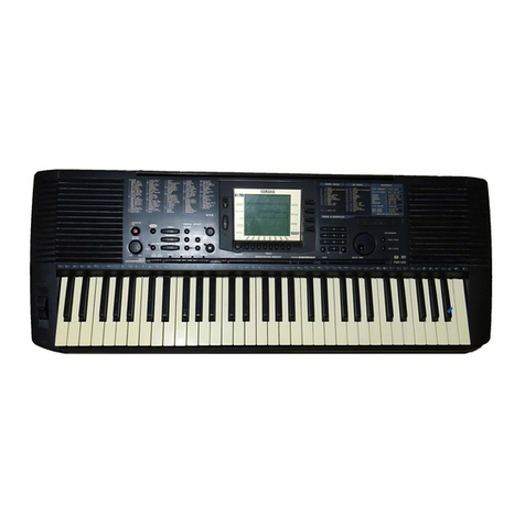
  9. Yamaha PortaTone PSR-1000 User manual

Yamaha PortaTone PSR-1000 User manual

Other manuals for PortaTone PSR-1000

4

This manual suits for next models

1

Other Yamaha Musical Instrument manuals

Yamaha Electone 305D User manual

Yamaha

Yamaha Electone 305D User manual

Yamaha RGX520FZ Series User manual

Yamaha

Yamaha RGX520FZ Series User manual

Yamaha Electone C-60 User manual

Yamaha

Yamaha Electone C-60 User manual

Yamaha YX-30GF User manual

Yamaha

Yamaha YX-30GF User manual

Yamaha Electone DK-40C User manual

Yamaha

Yamaha Electone DK-40C User manual

Yamaha ARIUS YDP-162B User manual

Yamaha

Yamaha ARIUS YDP-162B User manual

Yamaha PSR-E263 User manual

Yamaha

Yamaha PSR-E263 User manual

Yamaha YM-5104A User manual

Yamaha

Yamaha YM-5104A User manual

Yamaha DROP6 User manual

Yamaha

Yamaha DROP6 User manual

Yamaha Arius YDP-161 User manual

Yamaha

Yamaha Arius YDP-161 User manual

Yamaha YPR-9 Setup guide

Yamaha

Yamaha YPR-9 Setup guide

Yamaha AvantGrand N3X User manual

Yamaha

Yamaha AvantGrand N3X User manual

Yamaha N-100 User manual

Yamaha

Yamaha N-100 User manual

Yamaha RGX-612A User manual

Yamaha

Yamaha RGX-612A User manual

Yamaha P-125 User guide

Yamaha

Yamaha P-125 User guide

Yamaha Clavinova CVP-601 User manual

Yamaha

Yamaha Clavinova CVP-601 User manual

Yamaha AES920 Series User manual

Yamaha

Yamaha AES920 Series User manual

Yamaha CN-70 User manual

Yamaha

Yamaha CN-70 User manual

Yamaha YPP-35 User manual

Yamaha

Yamaha YPP-35 User manual

Yamaha YDP-301 User manual

Yamaha

Yamaha YDP-301 User manual

Yamaha PDP-500 User manual

Yamaha

Yamaha PDP-500 User manual

Yamaha P-60 User manual

Yamaha

Yamaha P-60 User manual

Yamaha Clavinova CLP-500 User manual

Yamaha

Yamaha Clavinova CLP-500 User manual

Yamaha Clavinova CLP-150 Installation and operation manual

Yamaha

Yamaha Clavinova CLP-150 Installation and operation manual

Popular Musical Instrument manuals by other brands

Funkey SP-561 user manual

Funkey

Funkey SP-561 user manual

thomann DP-275 GP BP user manual

thomann

thomann DP-275 GP BP user manual

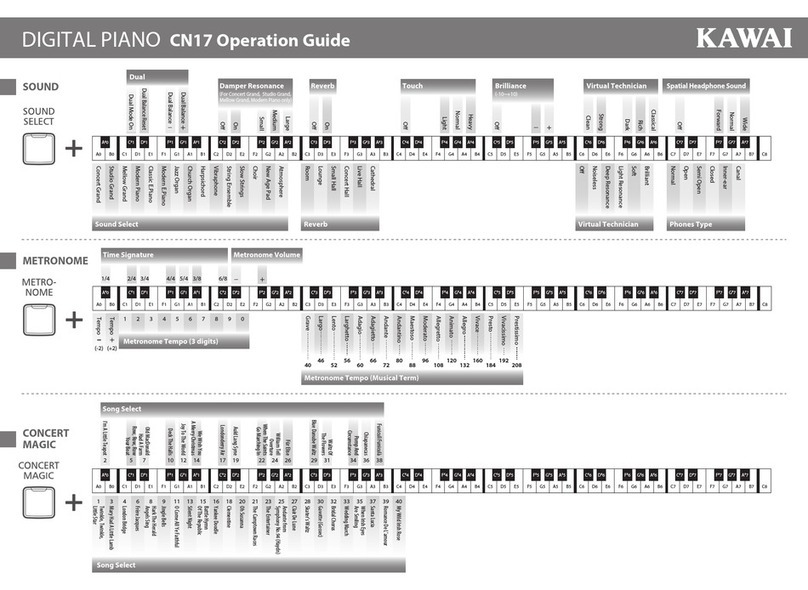
Kawai CN17 Operation guide

Kawai

Kawai CN17 Operation guide

Roland LX-15 Brochure & specs

Roland

Roland LX-15 Brochure & specs

Johannus Rembrandt 200 user manual

Johannus

Johannus Rembrandt 200 user manual

Casio celviano ap-700 user guide

Casio

Casio celviano ap-700 user guide

Modulus Quantum Series owner's manual

Modulus

Modulus Quantum Series owner's manual

Gear4music SDP-4 user manual

Gear4music

Gear4music SDP-4 user manual

HOMCOM 390-006 Assembly instruction

HOMCOM

HOMCOM 390-006 Assembly instruction

Xotic Guitars ProVintage Series owner's manual

Xotic Guitars

Xotic Guitars ProVintage Series owner's manual

Sadowsky MetroLine Series operating manual

Sadowsky

Sadowsky MetroLine Series operating manual

Bosendorfer CEUS user manual

Bosendorfer

Bosendorfer CEUS user manual

Alesis AHB-1 Assembly guide

Alesis

Alesis AHB-1 Assembly guide

Hotpoint RF512GP How to get the best

Hotpoint

Hotpoint RF512GP How to get the best

Roland V-Accordion FR-1x owner's manual

Roland

Roland V-Accordion FR-1x owner's manual

Samick DCP-12 manual

Samick

Samick DCP-12 manual

thomann DP-50 user manual

thomann

thomann DP-50 user manual

Artiphon INSTRUMENT 1 quick start guide

Artiphon

Artiphon INSTRUMENT 1 quick start guide

manuals.online logo
manuals.online logoBrands
  • About & Mission
  • Contact us
  • Privacy Policy
  • Terms and Conditions

Copyright 2025 Manuals.Online. All Rights Reserved.

PSR-2000
SERVICE MANUAL
PK 001666
HAMAMATSU, JAPAN
1.421K-4071 Printed in Japan '01.09
CONTENTS
SPECIFICATIONS···································································· 2
PANEL LAYOUT······································································· 4
CIRCUIT BOARD LAYOUT······················································ 6
DISASSEMBLY PROCEDURE················································· 8
LSI PIN DESCRIPTION·························································· 13
IC BLOCK DIAGRAM ····························································· 20
CIRCUIT BOARDS································································· 21
TEST PROGRAM··································································· 39
SYSTEM RESET···································································· 42
MIDI IMPLEMENTATION CHART·········································· 43
MIDI DATA FORMAT······························································ 44
PARTS LIST
BLOCK DIAGRAM
OVERALL CIRCUIT DIAGRAM
This document is printed on chlorine free (ECF) paper with soy ink.
PSR-1000
PIN
NO. I/O FUNCTIONNAME PIN
NO. I/O FUNCTIONNAME
1
2
3
4
5
6
7
8
9
10
11
12
AINR+
AINR-
VREF
VA
AGND
AINL+
AINL-
TST1
HPFE
TST2
TST3
VD
I
I
O
-
-
I
I
I/O
I/O
I/O
-
Analog signal input (R channel +)
Analog signal input (R channel -)
Reference voltage
Analog power supply
Analog ground
Analog signal input (L channel +)
Analog signal input (L channel -)
Test mode setting 1
HPF on/off
Test mode setting 2
Test mode setting 3
Digital power supply
13
14
15
16
17
18
19
20
21
22
23
24
DGND
TST4
AMODE2
/PD
MCLK
SCLK
LRCK
FSYNC
SDATA
CMODE
SMODE1
VB
-
I/O
I
I
I/O
I
I/O
O
I
I
-
Digital ground
Test mode setting 4
Interface clock select 2
Power-down mode
Master clock input
Serial data clock
Input/Output channel clock
Frame synch. clock
Serial data output
Master clock select
Interface clock select 1
Digital power supply
AK5351-VF-E2 (XV510A00) ADC (Analog to Digital Converter) DM: IC800 (PSR-2000)
PIN
NO. I/O FUNCTIONNAME PIN
NO. I/O FUNCTIONNAME
1
2
3
4
5
6
7
8
9
10
11
12
13
14
15
16
17
18
19
20
21
22
23
24
25
26
27
28
29
30
31
32
8"//5"
XTALSET
/RESET
E//RD
RW//WR
/CS
/DACK
RS0
RS1
VSS1
VSS2
D0
D1
D2
D3
D4
D5
D6
D7
/DREQ
/IRQ
/DEND
VSS3
1/2 EX1
VCC1
NUM1
NUM3
IFS
SFORM
/INP
/READY
/WPRT
I
I
I
I
I
I
I
I
I
I/O
I/O
I/O
I/O
I/O
I/O
I/O
I/O
O
O
I
I
I
I
I
I
I
I
Data transmission speed
Clock select
Rest
Enable/Read
Read/write/Write
Chip select
DMA acknowledge
Register select
Ground
Data bus
DMA request
Interrupt request
Data end
Ground
Power supply
Host interface select
Format data
Index pulse
Ready from FDD
Write control signal
33
34
35
36
37
38
39
40
41
42
43
44
45
46
47
48
49
50
51
52
53
54
55
56
57
58
59
60
61
62
63
64
/TRKO
/INDEX
/RDATA
XTAL2
EXTAL2
NC
XTAL1
EXTAL1
VSS4
VSS5
NC
VCC2
VCC3
VCC4
/WGATE
/WDATA
VSS6
/STEP
/HDIR
/HLOAD
/HSEL
VSS7
/DS0
/DS1
/DS2
/DS3
VSS8
/MON0
/MON1
/MON2
/MON3
VSS9
I
I
I
O
O
O
O
O
O
O
O
O
O
O
O
O
O
Track 00 signal
Index signal
Read data input from FDD
Clock
Clock
Ground
Power supply
Write control
Writ data to FDD
Ground
Step signal to control head of FDD
Direction
Head load
Head select
Ground
Drive select
Ground
Motor on
Ground
HD63266F (XI939A00) FDC (Floppy Disk Controller) DM: IC300
LSI PIN DESCRIPTION
PSR-1000/PSR-2000
13
HD63266F (XI939A00) FDC················································································································· 13
AK5351-VF-E2 (XV510A00) ADC ········································································································ 13
HD6417709F80B (XV250B00) CPU····································································································· 14
TC203C760HF-002 (XS725A00) SWP30B·························································································· 15
HG73C205AFD (XU947C00) SWX00B································································································ 16
YSS236-F (XT013A00) VOP3·············································································································· 17
µPD789022GB-A15-8E (XZ560100) CPU KBS···················································································· 18
S1D13305F00B100 (XQ595A00) LCDC ······························································································ 18
AD1854JRSRL (XY782A00) DAC········································································································ 19
PSR-1000/PSR-2000
14
PIN
NO. I/O FUNCTION
NAME PIN
NO. I/O FUNCTION
NAME
1
2
3
4
5
6
7
8
9
10
11
12
13
14
15
16
17
18
19
20
21
22
23
24
25
26
27
28
29
30
31
32
33
34
35
36
37
38
39
40
41
42
43
44
45
46
47
48
49
50
51
52
53
54
55
56
57
58
59
60
61
62
63
64
65
66
67
68
69
70
71
72
73
74
75
76
77
78
79
80
81
82
83
84
85
86
87
88
89
90
91
92
93
94
95
96
97
98
99
100
101
102
103
104
MD1
MD2
Vcc (RTC)
XTAL2
EXTAL2
Vss (RTC)
NMI
IRQ0/IRL0/PTH[0]
IRQ1/IRL1/PTH[1]
IRQ2/IRL2/PTH[2]
IRQ3/IRL3/PTH[3]
IRQ4/PTH[4]
D31/PTB[7]
D30/PTB[6]
D29/PTB[5]
D28/PTB[4]
D27/PTB[3]
D26/PTB[2]
Vss
D25/PTB[1]
Vcc
D24/PTB[0]
D23/PTA[7]
D22/PTA[6]
D21/PTA[5]
D20/PTA[4]
Vss
D19/PTA[3]
Vcc
D18/PTA[2]
D17/PTA[1]
D16/PTA[0]
Vss
D15
Vcc
D14
D13
D12
D11
D10
D9
D8
D7
D6
Vss
D5
Vcc
D4
D3
D2
D1
D0
A0
A1
A2
A3
Vss
A4
Vcc
A5
A6
A7
A8
A9
A10
A11
A12
A13
Vss
A14
Vcc
A15
A16
A17
A18
A19
A20
A21
Vss
A22
Vcc
A23
Vss
A24
Vcc
A25
BS/PTK[4]
RD
WE0/DQMLL
WE1/DQMLU/WE
WE2/DQMUL/ICIORD/PTK[6]
WE3/DQMUU/ICIOWR/PTK[7]
RD/WR
PTE[7]
Vss
CS0
Vcc
CS2/PTK[0]
CS3/PTK[1]
CS4/PTK[2]
CS5/CE1A/PTK[3]
CS6/CE1B
CE2A/PTE[4]
CE2B/PTE[5]
I
I
-
I
O
-
I
I
I
I
I
I
I/O
I/O
I/O
I/O
I/O
I/O
-
I/O
-
I/O
I/O
I/O
I/O
I/O
-
I/O
-
I/O
I/O
I/O
-
I/O
-
I/O
I/O
I/O
I/O
I/O
I/O
I/O
I/O
I/O
-
I/O
-
I/O
I/O
I/O
I/O
I/O
O
O
O
O
-
O
-
O
O
O
O
O
O
O
O
O
-
O
-
O
O
O
O
O
O
O
-
O
-
O
-
O
-
O
I/O
O
O
O
I/O
I/O
O
I/O
-
O
-
I/O
I/O
I/O
I/O
O
I/O
I/O
System clock
Power supply (3.3 V)
Clock
Clock
Ground (0 V)
Interrupt request
Interrupt request
Interrupt request
Data bus/ I/O port B
Ground (0 V)
Interrupt request
Power supply (3.3 V)
Data bus/ I/O port B
Data bus/ I/O port A
Ground (0 V)
Data bus/ I/O port A
Power supply (3.3 V)
Data bus/ I/O port A
Ground (0 V)
Data bus
Power supply (3.3 V)
Data bus
Ground (0 V)
Data bus
Power supply (3.3 V)
Data bus
Address bus
Ground (0 V)
Address bus
Power supply (3.3 V)
Address bus
Ground (0 V)
Address bus
Power supply (3.3 V)
Address bus
Ground (0 V)
Address bus
Power supply (3.3 V)
Address bus
Ground (0 V)
Address bus
Power supply (3.3 V)
Address bus
Bus control/ I/O port K
Read strobe
Select signal/DQM (SDRAM)
Select signal/DQM (SDRAM)/PCMCIA WE
Select signal/DQM (SDRAM)/PCMCIA I/O read/ I/O port K
Select signal/DQM (SDRAM)/PCMCIA I/O write/ I/O port K
Read/Write signal
I/O port E
Ground (0 V)
Chip select
Power supply (3.3 V)
Chip select/ I/O port K
Chip select/CE1/ I/O port K
Chip select/CE1
Chip enable/ I/O port E
105
106
107
108
109
110
111
112
113
114
115
116
117
118
119
120
121
122
123
124
125
126
127
128
129
130
131
132
133
134
135
136
137
138
139
140
141
142
143
144
145
146
147
148
149
150
151
152
153
154
155
156
157
158
159
160
161
162
163
164
165
166
167
168
169
170
171
172
173
174
175
176
177
178
179
180
181
182
183
184
185
186
187
188
189
190
191
192
193
194
195
196
197
198
199
200
201
202
203
204
205
206
207
208
CKE/PTK[5]
RAS3L/PTJ[0]
RAS2L/PTJ[1]
CASLL/CAS/PTJ[2]
Vss
CASLH/PTJ[3]
Vcc
CASHL/PTJ[4]
CASHH/PTJ[5]
DACK0/PTD[5]
DACK1/PTD[7]
CAS2L/PTE[6]
CAS2H/PTE[3]
RAS3U/PTE[2]
RAS2U/PTE[1]
PTE[0]
BACK
BREQ
WAIT
RESETM
PTH[5]/ADTRG
IOIS16/PTG[7]
PTG[6]
PTG[5]
PTG[4]
PTG[3]
PTG[2]
Vss
PTG[1]
Vcc
PTG[0]
PTF[7]/PINT[15]
PTF[6]/PINT[14]
PTF[5]/PINT[13]
PTF[4]/PINT[12]
PTF[3]/PINT[11]
PTF[2]/PINT[10]
PTF[1]/PINT[9]
PTF[0]/PINT[8]
MD0
Vcc (PLL1)
CAP1
Vss (PLL1)
Vss (PLL2)
CAP2
Vcc (PLL2)
PTH[6]
Vss
Vss
Vcc
XTAL
EXTAL
STATUS[0]/PTJ[6]
STATUS[1]/PTJ[7]
TCLK/PTH[7]
IRQOUT
Vss
CKIO
Vcc
TxD0/SCPT[0]
SCK0/SCPT[1]
TxD1/SCPT[2]
SCK1/SCPT[3]
TxD2/SCPT[4]
SCK2/SCPT[5]
RTS2/SCPT[6]
RxD0/SCPT[0]
RxD1/SCPT[2]
Vss
RxD2/SCPT[4]
Vcc
CTS2/IRQ5/SCPT[7]
PTC[7]/PINT[7]
PTC[6]/PINT[6]
PTC[5]/PINT[5]
PTC[4]/PINT[4]
Vss
WAKEUP/PTD[3]
Vcc
PTD[2]/RESETOUT
PTC[3]/PINT[3]
PTC[2]/PINT[2]
PTC[1]/PINT[1]
PTC[0]/PINT[0]
DRAK0/PTD[1]
DRAK1/PTD[0]
DREQ0/PTD[4]
DREQ1/PTD[6]
RESETP
CA
MD3
MD4
MD5
AVss
AN[0]/PTL[0]
AN[1]/PTL[1]
AN[2]/PTL[2]
AN[3]/PTL[3]
AN[4]/PTL[4]
AN[5]/PTL[5]
AVcc
AN[6]/DA[1]/PTL[6]
AN[7]/DA[0]/PTL[7]
AVss
I/O
I/O
I/O
I/O
-
I/O
-
I/O
I/O
I/O
I/O
I/O
I/O
I/O
I/O
I/O
O
I
I
I
I
I
I
I
I
I
I
-
I
-
I
I
I
I
I
I
I
I
I
I
-
-
-
-
-
-
I
-
-
-
O
I
I/O
I/O
I/O
O
-
I/O
-
O
I/O
O
I/O
I/O
I
-
I
-
I
I/O
I/O
I/O
I/O
-
I/O
-
I/O
I/O
I/O
I/O
I/O
I/O
I/O
I
I
I
I
I
I
I
-
I
I
I
I
I
I
-
I/O
I/O
-
CK enable (SDRAM)/ I/O port K
RAS/ I/O port J
RAS/ I/O port J
CAS (DRAM)/CAS (SDRAM)/ I/O port J
Ground (0 V)
CAS (DRAM)/ I/O port J
Power supply (3.3 V)
CAS (DRAM)/ I/O port J
DMAC/ I/O port D
DMAC/ I/O port D
CAS (DRAM)/ I/O port E
RAS/ I/O port E
RAS/ I/O port E
I/O port E
System clock
System clock
Bus control
Reset
I/O port H/Analog
Right protect/Input port G
I/O port G
Ground (0 V)
I/O port G
Power supply (3.3 V)
I/O port G
I/O port F/Port Interrupt request
System clock
Power supply (3.3 V)
Clock
Ground (0 V)
Ground (0 V)
Clock
Power supply (3.3 V)
I/O port H
Ground (0 V)
Ground (0 V)
Power supply (3.3 V)
Clock
Clock
System clock
Timer
Interrupt request
Ground (0 V)
Clock
Power supply (3.3 V)
Forward data/Output port for SCI
Serial clock/ I/O port for SCI
Forward data/Output port for SCI
Serial clock/ I/O port for SCI
Transmit request/ I/O port for SCI
Reception data/Input port for SCI
Ground (0 V)
Reception data/Input port for SCI
Power supply (3.3 V)
Transmit clear/Interrupt request/Input port for SCI
I/O port C/Interrupt request
Ground (0 V)
Interrupt request/ I/O port D
Power supply (3.3 V)
I/O port D/Reset
I/O port C/Interrupt request
DMA request/ I/O port D
System clock
System clock
System clock
System clock
System clock
Analog ground (0 V)
A/D change input/Input port L
Analog power supply (3.3 V)
A/D change input/D/A change output/Input port L
Analog ground (0 V)
HD6417709F80B (XV250B00) CPU DM: IC100
PSR-1000/PSR-2000
15
PIN
NO. I/O FUNCTION
NAME PIN
NO. I/O FUNCTION
NAME
1
2
3
4
5
6
7
8
9
10
11
12
13
14
15
16
17
18
19
20
21
22
23
24
25
26
27
28
29
30
31
32
33
34
35
36
37
38
39
40
41
42
43
44
45
46
47
48
49
50
51
52
53
54
55
56
57
58
59
60
61
62
63
64
65
66
67
68
69
70
71
72
73
74
75
76
77
78
79
80
81
82
83
84
85
86
87
88
89
90
91
92
93
94
95
96
97
98
99
100
101
102
103
104
105
106
107
108
109
110
111
112
113
114
115
116
117
118
119
120
Vss
CA0
CA1
CA2
CA3
CA4
CA5
CA6
CA7
CA8
CA9
CA10
CA11
VSS
CD0
CD1
CD2
CD3
CD4
CD5
CD6
CD7
CD8
CD9
CD10
CD11
CD12
CD13
CD14
VDD
VSS
CD15
CSN
WRN
RDN
VDD
SYSH0
SYSH1
SYSH2
SYSH3
SYSH4
SYSH5
SYSH6
SYSH7
KONO0
KONO1
KONO2
KONO3
VSS
SYSL0
SYSL1
SYSL2
SYSL3
SYSL4
SYSL5
SYSL6
SYSL7
KONI0
KONI1
VDD
VSS
KONI2
KONI3
DAC0
DAC1
WCLK
MELO0
MELO1
MELO2
MELO3
MELO4
MELO5
MELO6
MELO7
VDD
ADLR
MELI0
MELI1
MELI2
MELI3
MELI4
MELI5
MELI6
MELI7
VSS
RCASN
RA8
RA7
RA6
VDD
VSS
RA5
RA4
RA3
RA2
RA1
RA0
RRASN
RWEN
VSS
RD7
RD6
RD5
RD4
RD3
RD2
RD1
RD0
VSS
RD17
RD16
RD15
RD14
RD13
RD12
RD11
RD10
RD9
RD8
VDD
I
I
I
I
I
I
I
I
I
I
I
I
I/O
I/O
I/O
I/O
I/O
I/O
I/O
I/O
I/O
I/O
I/O
I/O
I/O
I/O
I/O
I/O
I
I
I
O
O
O
O
O
O
O
O
O
O
O
O
I/O
I/O
I/O
I/O
I/O
I/O
I/O
I/O
I
I
I
I
I
O
O
O
O
O
O
O
O
O
O
O
O
I
I
I
I
I
I
I
I
O
O
O
O
O
O
O
O
O
O
O
O
I/O
I/O
I/O
I/O
I/O
I/O
I/O
I/O
I/O
I/O
I/O
I/O
I/O
I/O
I/O
I/O
I/O
I/O
(Ground)
Address bus of internal register
(Ground)
Data bus of internal register
(Power supply)
(Ground)
Chip select
Write strobe
Read strobe (Power supply)
NSYS/LNSYS upper 16 bits
Key on data
(Ground)
NSYS input/LNSYS output lower 8 bits
(Power supply)
Key on data input (Ground)
DAC output
DAC0/DAC1 word clock
MEL wave data output
(Power supply)
ADC word clock
MEL wave data input
(Ground)
DRAM column address strobe
(Power supply)
(Ground)
DRAM address bus
DRAM row address strobe
DARM write enable (Ground)
(Ground)
DRAM data bus
(Power supply)
121
122
123
124
125
126
127
128
129
130
131
132
133
134
135
136
137
138
139
140
141
142
143
144
145
146
147
148
149
150
151
152
153
154
155
156
157
158
159
160
161
162
163
164
165
166
167
168
169
170
171
172
173
174
175
176
177
178
179
180
181
182
183
184
185
186
187
188
189
190
191
192
193
194
195
196
197
198
199
200
201
202
203
204
205
206
207
208
209
210
211
212
213
214
215
216
217
218
219
220
221
222
223
224
225
226
227
228
229
230
231
232
233
234
235
236
237
238
239
240
VSS
HMD0
HMD1
HMD2
HMD3
HMD4
HMD5
HMD6
HMD7
HMD8
HMD9
HMD10
HMD11
HMD12
HMD13
HMD14
HMD15
VSS
HMA0
HMA1
HMA2
HMA3
HMA4
HMA5
HMA6
HMA7
HMA8
HMA9
HMA10
VSS
VDD
HMA11
HMA12
HMA13
HMA14
HMA15
HMA16
HMA17
HMA18
HMA19
HMA20
HMA21
HMA22
HMA23
HMA24
VSS
MRASN
MCASN
MOEN
MWEN
VSS
LMD0
LMD1
LMD2
LMD3
LMD4
LMD5
LMD6
LMD7
VDD
VSS
LMD8
LMD9
LMD10
LMD11
LMD12
LMD13
LMD14
LMD15
VSS
LMA0
LMA1
LMA2
LMA3
LMA4
LMA5
LMA6
LMA7
LMA8
LMA9
LMA10
LMA11
VSS
LMA12
LMA13
LMA14
LMA15
LMA16
LMA17
VDD
VSS
LMA18
LMA19
LMA20
LMA21
LMA22
LMA23
LMA24
VSS
SYO
SYOD
QCLK
HCLK
CK256
SYSCLK
VDD
SYI
MCLKI
MCLKO
VDD
XIN
XOUT
VSS
ICN
CHIP2
SLAVE
TESTON
ACIN
DCTEST
VDD
I/O
I/O
I/O
I/O
I/O
I/O
I/O
I/O
I/O
I/O
I/O
I/O
I/O
I/O
I/O
I/O
O
O
O
O
O
O
O
O
O
O
O
O
O
O
O
O
O
O
O
O
O
O
O
O
O
O
O
O
O
I/O
I/O
I/O
I/O
I/O
I/O
I/O
I/O
I/O
I/O
I/O
I/O
I/O
I/O
I/O
I/O
O
O
O
O
O
O
O
O
O
O
O
O
O
O
O
O
O
O
O
O
O
O
O
O
O
O
O
O
O
O
O
I
I
O
I
O
I
I
I
I
I
I
(Ground)
Wave memory data bus (Upper data memory)
(Ground)
(Ground)
(Power supply)
Wave memory address bus (Upper 16 bits)
(Ground)
RAS when DRAM(s) is connected to wave memory
CAS when DRAM(s) is connected to wave memory
Wave memory output enable
Wave memory write enable (Ground)
Wave memory data bus (Lower data memory)
(Power supply)
(Ground)
(Ground)
(Ground)
Wave memory address bus (Lower data memory)
(Power supply)
(Ground)
(Ground)
Sync. signal for master clock
Sync. signal for HCLK/QCLK
1/12 master clock (64 Fs)
1/6 master clock (128 Fs)
1/3 master clock (256 Fs)
1/2 master clock (384 Fs) (Power supply)
Sync. clock
Master clock input
Master clock output (Power supply)
Crystal osc. input
Crystal osc. output (Ground)
Initial clear
2 chips mode enable
Master/Slave select when 2 chips mode
Test pin
(Power supply)
TC203C760HF-002 (XS725A00) SWP30B (AWM Tone Generator coped with MEG)
Standard Wave Processor DM: IC400 (PSR-2000 only)
PIN
NO. I/O FUNCTIONNAME PIN
NO. I/O FUNCTIONNAME
1
2
3
4
5
6
7
8
9
10
11
12
13
14
15
16
17
18
19
20
21
22
23
24
25
26
27
28
29
30
31
32
33
34
35
36
37
38
39
40
41
42
43
44
45
46
47
48
49
50
51
52
53
54
55
56
57
58
59
60
61
62
63
64
65
66
67
68
69
70
71
72
73
74
75
76
77
78
79
80
81
82
83
84
ICN
RFCLKI
TM2
AVDD_PLL
AVSS_PLL
MODE0
VCC7
GND8
XIN
XOUT
MODE1
TEST0
TESTON
AN0-P40
AN1-P41
AN2-P42
AN3-P43
AVDD_AN
AVSS_AN
TXD0
TXD1
EXCLK
SMD11
SMD4
SMD3
SMD12
SMD10
SMD5
SMD2
SMD13
SMD9
SMD6
SMD1
SMD14
VCC35
GND36
SMD8
SMD7
SMD0
SMD15
SOE
SWE
SRAS
SCAS
REFRESH
CS0
SMA0
SMA16
VCC49
GND50
SMA1
SMA15
SMA2
SMA14
SMA3
SMA13
SMA4
SMA12
SMA5
GND60
VCC61
SMA11
SMA6
SMA10
SMA7
SMA9
SMA17
SMA8
SMA18
SMA19
SMA20
SMA21
SMA22
SMA23
CMA20
CMA19
VCC77
GND78
CMA18
CMA17
CMA5
CMA6
CMA4
CMA7
I
I
I
I
I
O
I
I
I
I
I
I
I
O
O
I
I/O
I/O
I/O
I/O
I/O
I/O
I/O
I/O
I/O
I/O
I/O
I/O
I/O
I/O
I/O
I/O
O
O
O
O
O
O
O
O
O
O
O
O
O
O
O
O
O
O
O
O
O
O
O
O
O
O
O
O
O
O
O
O
O
O
O
O
O
O
O
Initial clear
PLL Clock
PLL Control
Power supply
Ground
SWX dual mode
Power supply
Ground
crystal oscillator
crystal oscillator
SWX separate mode
TEST pin
TEST pin
A/D converter
A/D converter
A/D converter
A/D converter
Power supply
Ground
for MIDI or TO-HOST
for MIDI
Crystal oscillator
Wave memory data bus
Power supply
Ground
Wave memory data bus
read signal
write signal
RAS signal
CAS signal
REFRESH signal
CS signal
Memory address bus
Memory address bus
Power supply
Ground
Memory address bus
Memory address bus
Memory address bus
Memory address bus
Memory address bus
Memory address bus
Memory address bus
Memory address bus
Memory address bus
Ground
Power supply
Memory address bus
Memory address bus
Memory address bus
Memory address bus
Memory address bus
Memory address bus
Memory address bus
Memory address bus
Memory address bus
Memory address bus
Memory address bus
Memory address bus
Memory address bus
Program address bus
Program address bus
Power supply
Ground
Program address bus
Program address bus
Program address bus
Program address bus
Program address bus
Program address bus
85
86
87
88
89
90
91
92
93
94
95
96
97
98
99
100
101
102
103
104
105
106
107
108
109
110
111
112
113
114
115
116
117
118
119
120
121
122
123
124
125
126
127
128
129
130
131
132
133
134
135
136
137
138
139
140
141
142
143
144
145
146
147
148
149
150
151
152
153
154
155
156
157
158
159
160
161
162
163
164
165
166
167
168
CMA3
CMA8
CMA2
CRD
CMA1
CUB
VCC91
GHND92
CS1
CMA0
CLB
CMA12
CMA11
CMA10
CMA9
GND100
CWE
CMA16
CMA15
CMA14
CMA13
CMD8
CMD7
CMD9
CMD6
CMD10
CMD5
CMD11
CMD4
CMD12
CMD3
CMD13
CMD2
CMD14
VCC119
GND115
CMD1
CMD15
CMD0
CMA21
PDT15
PDT14
PDT13
PDT12
PDT11
PDT10
PDT9
PDT8
VCC133
GND134
PDT7
PDT6
PDT5
PDT4
PDT3
PDT2
PDT1
PDT0
VCA143
GND144
PAD2
PAD1
PAD0
VCC148
GND149
PCS
PWR
PRD
RXD0
RXD1
SCLKI
ADIN
ADLR
DO0
DO1
SYSCLK
VCC161
GND162
WCLK
QCLK
BCLK
SYI
IRQ0
NMI
O
O
O
O
O
O
O
O
O
O
O
O
O
O
O
O
O
O
I/O
I/O
I/O
I/O
I/O
I/O
I/O
I/O
I/O
I/O
I/O
I/O
I/O
I/O
I/O
I/O
O
I/O
I/O
I/O
I/O
I/O
I/O
I/O
I/O
I/O
I/O
I/O
I/O
I/O
I/O
I/O
I/O
I
I
I
I
I
I
I
I
I
I
O
O
O
O
O
O
O
I
I
I
Program address bus
Program address bus
Program address bus
read signal
Program address bus
high byte effective signal
Power supply
Ground
CS signal
Program address bus
low byte effective signal
Program address bus
Program address bus
Program address bus
Program address bus
Ground
write signal
Program address bus
Program address bus
Program address bus
Program address bus
Program memory Data bus
Power supply
Ground
Program memory Data bus
Program address bus
SWX access data bus
SWX access data bus
SWX access data bus
SWX access data bus
SWX access data bus
SWX access data bus
SWX access data bus
SWX access data bus
Power supply
Ground
SWX access data bus
SWX access data bus
SWX access data bus
SWX access data bus
SWX access data bus
SWX access data bus
SWX access data bus
SWX access data bus
Power supply
Ground
SWX access address bus
Power supply
Ground
Chip select
write enable
read enable
for Midi or TO-HOST
for Midi or Key scan
EXT Clock
A/D converter
A/D converter LR clock
DAC
DAC
1/2 clock
Power supply
Ground
for DAC LR clock
1/12 clock
IIS-DAC clock
Synch signal
Interrupt request
Interrupt request
HG73C205AFD (XU947C00) SWX00B (Tone Generator) DM: IC801 (PSR-1000)
PSR-1000/PSR-2000
16
PSR-1000/PSR-2000
17
PIN
NO. I/O FUNCTIONNAME PIN
NO. I/O FUNCTIONNAME
1
2
3
4
5
6
7
8
9
10
11
12
13
14
15
16
17
18
19
20
21
22
23
24
25
26
27
28
29
30
31
32
33
34
35
36
37
38
39
40
41
42
43
44
45
46
47
48
49
50
51
52
53
54
55
56
57
58
59
60
61
62
63
64
65
66
67
68
69
70
71
72
73
74
75
76
77
78
79
80
VSS
WA17
WA16
WA15
WA14
WA13
WA12
WA11
WA10
VDD
VSS
WA09
WA08
WA07
WA06
WA05
WA04
WA03
WA02
VDD
VSS
WA01
WA00
WEN
OEN
RASN
CASN
CEN
VDD
VSS
WD19
WD18
WD17
WD16
WD15
WD14
VDD
VSS
WD13
WD12
WD11
WD10
WD09
WD08
WD07
VDD
VSS
WD06
WD05
WD04
WD03
WD02
WD01
WD00
VDD
VSS
TST2
TST1
TST0
MS
LRCLK
SI7
SI6
VDD
VSS
SI5
SI4
SI3
SI2
SI1
SI0
DB1
DB0
VDD
VSS
ODFM
OFS3
OFS2
OFS1
OFS0
O
O
O
O
O
O
O
O
O
O
O
O
O
O
O
O
O
O
O
O
O
O
I/O
I/O
I/O
I/O
I/O
I/O
I/O
I/O
I/O
I/O
I/O
I/O
I/O
I/O
I/O
I/O
I/O
I/O
I/O
I/O
O
O
O
I
O
I
I
I
I
I
I
I
I
I
I
I
I
I
I
I
Power supply
External memory address bus
Ground
Power supply
External memory address bus
Ground
Power supply
External memory address bus
External memory control (WEN)
External memory control (OEN)
External memory control (RASN)
External memory control (CASN)
External memory control (CEN)
Ground
Power supply
External memory data bus
Ground
Power supply
External memory data bus
Ground
Power supply
External memory data bus
Ground
Power supply
Test output
Memory select
LR clock for ADC
Serial input
Ground
Power supply
Serial input
Output bit type select for DAC
Ground
Power supply
Output mode select for DAC
Serial output format select
81
82
83
84
85
86
87
88
89
90
91
92
93
94
95
96
97
98
99
100
101
102
103
104
105
106
107
108
109
110
111
112
113
114
115
116
117
118
119
120
121
122
123
124
125
126
127
128
129
130
131
132
133
134
135
136
137
138
139
140
141
142
143
144
145
146
147
148
149
150
151
152
153
154
155
156
157
158
159
160
SO7
SO6
SO5
VDD
VSS
SO4
SO3
SO2
SO1
SO0
WDCK
SWPKON
IRQN
VDD
VSS
XTAL_I
XTAL_O
MCLK
VDD
VSS
MICN
CLKIN
SYWIN
SYW
SYWD
VDD
VSS
CLKO
WCLK
HCLK
QCLK
TSTCI
VDD
VSS
(NC)
VDD(PLL)
CPO
CPIN
REF
VSS(PLL)
(NC)
VDD
VSS
TSTCS
CA6
CA5
CA4
CA3
CA2
VDD
VSS
CA1
CA0
CSN
RDN
WRN
BTYP
VDD
VSS
CD15
CD14
CD13
CD12
CD11
VDD
VSS
CD10
CD09
CD08
CD07
CD06
CD05
VDD
VSS
CD04
CD03
CD02
CD01
CD00
VDD
O
O
O
O
O
O
O
O
O
O
O
I
O
O
I
I
I
O
O
O
O
O
O
I
O
I
I
I
I
I
I
I
I
I
I
I
I
I
I/O
I/O
I/O
I/O
I/O
I/O
I/O
I/O
I/O
I/O
I/O
I/O
I/O
I/O
I/O
I/O
Serial output
Ground
Power supply
Serial output
Data enable for DAC
SWP00 format key on output
EG interrupt
Ground
Power supply
Quartz crystal terminal
Oscillate clock output
Ground
Power supply
Initial clear
Master clock input
Sync.signal input
Sync.signal output
Sync.signal output
Ground
Power supply
For test (512 fs output)
2 times sync.clock output (256 fs)
4 times sync.clock output (128 fs)
8 times sync.clock output (64 fs)
PLL test input
Ground
Power supply
PLL control output
PLL control input
PLL control input
Ground
Power supply
PLL test input
CPU address bus
Ground
Power supply
CPU address bus
Lo/Hi select in 8 bits write
Chip select
Register read
Register write
Data bus type select
Ground
Power supply
CPU data bus
Ground
Power supply
CPU data bus
Ground
Power supply
CPU data bus
Ground
YSS236-F (XT013A00) VOP3 DM: IC401 (PSR-2000 only)
PSR-1000/PSR-2000
18
PIN
NO. I/O FUNCTIONNAME PIN
NO. I/O FUNCTIONNAME
1
2
3
4
5
6
7
8
9
10
11
12
13
14
15
16
17
18
19
20
21
22
23
24
25
26
27
28
29
30
VA5
VA4
VA3
VA2
VA1
VA0
/VWR
/VCE
/VRD
/RES
NC
NC
/RD
/WR
SEL2
SEL1
OSC1
OSC2
/CS
A0
Vdd
D0
D1
D2
D3
D4
D5
D6
D7
XD3
O
O
O
O
O
O
O
O
-
I
-
-
I
I
I
I
I
O
I
I
-
I/O
I/O
I/O
I/O
I/O
I/O
I/O
I/O
O
VRAM address bus
VRAM read/write
Memory control
Not used
Initial clear
Not used
Not used
Read strobe
Write strobe
Bus select
Bus select
Clock
Clock
Chip select
Data mode select
Power supply
Data bus
Data bus output for 4 bit dot
31
32
33
34
35
36
37
38
39
40
41
42
43
44
45
46
47
48
49
50
51
52
53
54
55
56
57
58
59
60
XD2
XD1
XD0
XECL
XSCL
Vss
LP
WF
YDIS
YD
YSCL
VD7
VD6
VD5
VD4
VD3
VD2
VD1
VD0
VA15
VA14
VA13
VA12
VA11
VA10
VA9
VA8
VA7
VA6
NC
O
O
O
O
O
-
O
O
O
O
O
I/O
I/O
I/O
I/O
I/O
I/O
I/O
I/O
O
O
O
O
O
O
O
O
O
O
-
Data bus output for 4 bit dot
S driver enable, chain clock
Data bus shift clock
Ground
X driver latch pulse
Frame signal for X/Y driver
Power down signal for displaying off mode
Scan start signal
Scan shift clock
VRAM data bus
VRAM address bus
Not used
S1D13305F00B100 (XQ595A00) LCDC (LCD Controller) DM: IC500
PIN
NO. I/O FUNCTIONNAME PIN
NO. I/O FUNCTIONNAME
1
2
3
4
5
6
7
8
9
10
11
12
13
14
15
16
17
18
19
20
21
22
P12
P11
P10
P47/KR7
P46/KR6
P45/KR5
P44/KR4
P43/KR3
P42/KR2
P41/KR1
P40/KR0
NC
IC
X2
X1
VSS0
VDD0
/RESET
P53
P52
P51/TO2
P50/TI0/TO0
I/O
I/O
I/O
I/O
I/O
I/O
I/O
I/O
I/O
I/O
I/O
I
I
I/O
I/O
I/O
I/O
Port 1
Port 4/Key return signal detection input
Internally connected (N.C.)
Clock
Ground
Power supply
System reset
Port 5
Port 5/16-bit timer output
Port 5/External count clock input to 8-bit timer/8-bit timer output
23
24
25
26
27
28
29
30
31
32
33
34
35
36
37
38
39
40
41
42
43
44
P32/INTP2/CPT2
P31/INTP1
P30/INTP0
P22/RXD/SI0
P21/TXD/SO0
P20/ASCK//SCK0
P07
P06
P05
P04
P03
P02
P01
P00
NC
VDD1
VSS1
P17
P16
P15
P14
P13
I/O
I/O
I/O
I/O
I/O
I/O
I/O
I/O
I/O
I/O
I/O
I/O
I/O
I/O
I/O
I/O
I/O
I/O
I/O
Port 3/External interrupt input/Capture edge input
Port 3/External interrupt input
Port 2/Asynchronous serial interface serial data input/Serial interface serial data input
Port 2/Asynchronous serial interface serial data output/Serial interface serial data output
Port 2/Asynchronous serial interface serial clock input/Serial interface serial clock
Port 0
Power supply
Ground
Port 1
µPD789022GB-A15-8E
(XZ560100) CPU
MKS5F: IC1
PSR-1000/PSR-2000
19
PIN
NO. I/O FUNCTIONNAME PIN
NO. I/O FUNCTIONNAME
1
2
3
4
5
6
7
8
9
10
11
12
13
14
DGND
MCLK
CLATCH
CCLK
CDATA
384//256
X2MCLK
ZEROR
DEEMP
96//48
AGND
OUTR+
OUTR-
FILTR
I
I
I
I
I
I
I
O
I
I
I
O
O
O
Digital Ground
Master Clock Input. Connect to an external
clock source at either 256, 384 or 512 Fs.
Latch input for control data. This input is
rising-edge sensitive.
Control clock input for control data. Control
input data must be valid on the rising edge of
CCLK. CCLK may be continuous or gated.
Serial control input, MSB first, containing 16 bits
of unsigned data per channel. Used for specifying
channel-specific attenuation and mute.
Selects the master clock mode as either 384
times the intended sample frequency (HI) or
256 times the intended sample frequency (LO).
The state of this input should be hardwired to
logic HI or logic LO, or may be changed while
the AD1854 is in power-down/reset. It must not
be changed while the AD1854 is operational.
Selects internal clock doubler (LO) or
internal clock = MCLK (HI).
Right Channel Zero Flag Output. This pin
goes HI when Right Channel has no signal
input for more than 1024 LR Clock Cycles.
De-Emphasis. Digital de-emphasis is
enabled when this input signal is HI. This is
used to impose a 50 µs/15 µs response
characteristic on the output audio spectrum
at an assumed 44.1 kHz sample rate.
Selects 48 kHz (LO) or 96 kHz Sample
Frequency Control.
Analog Ground
Right Channel Positive line level analog output.
Right Channel Negative line level analog output.
Voltage Reference Filter Capacitor Connection.
Bypass and decouple the voltage reference
with parallel 10 µF and 0.1 µF capacitors to the
AGND.
15
16
17
18
19
20
21
22
23
24
25
26
27
28
AGND
OUTL-
OUTL+
AVDD
FILTB
IDPM1
IDPM0
ZEROL
MUTE
/PD//RST
L//RCLK
BCLK
SDATA
DVDD
I
O
O
I
O
I
I
O
I
I
I
I
I
I
Analog Ground
Left Channel Negative line level analog
output.
Left Channel Positive line level analog
output.
Analog Power Supply. Connect to analog 5
V supply.
Filter Capacitor connection, connect 10 µF
capacitor to AGND.
Input serial data port mode control one.
With IDPM0, defines one of four serial
modes.
Input serial data port mode control zero.
With IDPM1, defines one of four serial
modes.
Left Channel Zero Flag Output. This pin
goes HI when Left Channel has no signal
input for more than 1024 LR Clock Cycles.
Mute. Assert HI to mute both stereo analog
outputs. Deassert LO for normal operation.
/Power-Down//Reset. The AD1854 is
placed in a low power consumption mode
when this pin is held LO. The AD1854 is
reset on the rising edge of this signal. The
serial control port registers are reset to the
default values. Connect HI for normal
operation.
Left//Right clock input for input data. Must
run continuously.
Bit clock input for input data. Need not run
continuously; may be gated or used in a
burst fashion.
Serial input, MSB first, containing two
channels of 16, 18, 20, and 24 bits of twos
complement data per channel.
Digital Power Supply Connect to digital 5 V
supply.
AD1854JRSRL (XY782A00) DAC (Digital to Analog Converter) DM: IC700
1
2
3
4
5
6
7
1A
1Y
2A
2Y
3A
3Y
Vss
14
13
12
11
10
9
8
VDD
6A
6Y
5A
5Y
4A
4Y
SN74HCU04NSR (XW842A00)
SN74HCU04N (IG142250)
Hex Inverter
DM:
AM:
HD74LV08AFPEL (IS000800)
Quad 2 Input AND
DM: IC101
HD74LV21ATELL (X0010A00)
Dual 4 Input AND
DM: IC310
SN74HC132NSR (XW792A00)
MM74HC132SJX (XY352A00)
Quad 2 Input NAND
DM: IC914
SN74HCT138NSR (XY865A00)
3 to 8 Demultiplexer
DM: IC600
HD74LVC139FPEL (XS048A00)
Dual 2 to 4 Demultiplexer
DM: IC308
HD74LV245ATELL (XW744A00)
74LVC245APW (XZ286A00)
TC74VHCT245AFT (XT744A00)
Octal 3-State Bus Transceiver
DM: IC103, 104, 301-303, 304-306, 911
SN75C1168N (XU463A00)
Line Driver/Receiver
AM: IC307
M5227P (XF751A00)
5-Band Graphic Equalizer
AM: IC104, 105
IC510, 511
IC301
1
2
3
1A
1Y
4
2A
5
2B
6
2Y
VSS 7
1B
14
13
12
VDD
4A
11 4Y
10 3B
93A
83Y
4B
1
2
3
1A
NC
4
1C
5
1D
6
1Y
7
GND
1B
14
13
12
Vcc
2C
11 NC
10 2B
92A
82Y
2D
1
2
3
1A
1Y
4
2Y
5
2A
6
2B
7
GND
1B
14
13
12
VDD
4A
11 4Y
10 3Y
93B
83A
4B
1
2
3
4
5
6
7
A
B
C
G2A
G2B
G1
Y7 Y5
Y4
Y3
Y2
Y1
Y0
Y6
16
15
14
13
12
11
10
89
Enable
Output
Output
Select
A
B
C
G2A
G2B
Y7
GND
G1
Vcc
YO
Y1
Y2
Y3
Y5
Y6
Y4
1
2
3
4
5
6
7
1G
1A
1B
1Y0
1Y1
1Y2
1Y3
AG
B
Y0
Y1
Y2
Y3
16
15
14
13
12
11
10
Vcc
2G
2A
2B
2Y0
2Y1
2Y2
8
GND 92Y3
Y2
Y3
Y1
Y0
B
A
G
1
2
3
4
5
6
7
20
19
18
17
16
15
14
Vcc
G
B1
B2
B3
B4
B5
B6
B7
B8
8
9
10
12
11
GND
A8
A7
A6
A5
A4
A3
A2
A1
D1R
13
1
2
3
4
5
6
7
1B
1A
1R
1DE
2R
2A
2B
16
15
14
13
12
11
10
Vcc
1D
1Y
1Z
2DE
2Z
2Y
8
GND 92D
1
2
3
4
5
6
7
IN1
NF1
IN2
NF2
IN3
NF3
IN4
16
15
14
13
12
11
10
-Vcc
GND
+Vcc
OUT
-IN
10k
10k
47k
47k
47k540
540
540
540
540
540
47k
47k
47k +IN
NF5
8
NF4 9IN5
+-
+-
+-
+-
+-
+-
PSR-1000/PSR-2000
20
IC BLOCK DIAGRAM
TEST PROGRAM
PSR-1000/PSR-2000
39
1. Preparation
1) PA-300 (AC adaptor) is used.
2) The volume is usually moved to the use position when no volume change is required.
3) Measuring instruments: frequency counter, level meter (with JIS-C filter)
Note: Connect a stereo plug to the [PHONES] jack at 33 ohms.
4) Jigs: foot switch (FC-4), foot volume (FC-7), MIDI cable, floppy disk (2HD & 2DD), microphone (PSR-2000 only)
2. How to enter the Test Program
While pressing the [C#2], [F2] and [G#2] keys, turn the [STANDBY/ON] switch on.
3. Proceeding through the Teat Program
When the test program is activated, the sign “TEST” is indicated on the LCD display.
Automatically performs RAM BACKUP check when entering test mode.
Select the test program item to be executed by pressing the [TEMPO-] or [TEMPO+] button.
Press the [START/STOP] button to execute testing. When the test result is OK, press the [START/STOP] button to return to the test
item name on display. Proceed to the next test by pressing the [TEMPO-] or [TEMPO+] button. When the test result is OK, an asterisk
(*) is added in front of its item name on display.
When the test result is NG, press the [DEMO] button or the lowest (leftmost) white key on the keyboard to return to the test item name
on display and then turn off the [STANDBY/ON] switch to end the test program.
4. Test program list
No. LCD (initial) Test Function and Judgment criteria
1
2
3
4
5
6
7
9
10
12
15
001: Version
002: ROM Check1
003: RAM Check1
004:Flash Check1
005: Wave ROM Check1
006: Wave RAM Check1
007: FDD Check
009: Effect 2 RAM Check
(PSR-2000 only)
010: Effect 3 RAM Check
012: TG1 Check
015: Pitch Check
Displays each ROM version.
ROM versions are displayed alternately on the LCD.
Checks the ROMs that are connected to the CPU bus.
The test results appear on the LCD. Check the LCD “ROM Check1 OK”
Checks the RAMs that are connected to the CPU bus.
The test results appear on the LCD. Check the LCD “RAM Check1 OK”
Checks the Flash Memories that are connected to the CPU bus.
The test results appear on the LCD. Check the LCD “Flash Check1 OK”
Checks the Wave ROMs.
The test results appear on the LCD. Check the LCD “XG Wave ROM Check OK”
Checks the Wave RAMs.
The test results appear on the LCD. Check the LCD “XG Wave RAM Check OK”
Checks the floppy disk drive unit.
Insert the floppy disks one bye one (2HD or 2DD).
The test will be executed immediately if an FD is inserted in the drive. After completing the test for one FD,
replace it with another to continue the test.
Displays “FDD Check OK” if the test result is OK.
Displays “NO FD” and stands by for FD insertion if an FD is drawn out before completion of the test.
Displays “PROTECT FD” if the write-protect switch of FD is on.
Displays “UNFORMAT FD” if non-formatted FD is inserted.
Checks the VOP3 RAM.
Outputs the sine wave (C3) MAX at the send level and MIN at the drive level.
Check the sound by hearing that there is not noise or abnormal sound.
Checks the XG1 RAM.
Outputs the sine wave (C3) MAX at the send level and MIN at the drive level.
Check the sound by hearing that there is not noise or abnormal sound.
Sequentially outputs the sine wave starting from the low keys (from C2 to G4) by switching the channel of the
sound source.
Check the sound by hearing that there is not noise or abnormal sound.
Pitch check: Connect the frequency counter to the [PHONES] jack (33 ohm load).
Outputs the sine wave at 440.0 Hz +/- 0.22 Hz. (PAN = Center)
Decline quantity check of the volume: Connect the level meter (with JIS-C filter) to the [PHONES] jack. Set the
[MASTER VOLUME] at MIN and check the output level.
PHONES L, R: less than -80.0 dBm