SPECIFICATIONS
MD4S
6
Recorder
Mixer
General
Digital/Audio
Rec/Play
Locate
Cue & review
Disc Editing
Song Editing
Track Editing
Title Editing
Panel Controls
MIDI
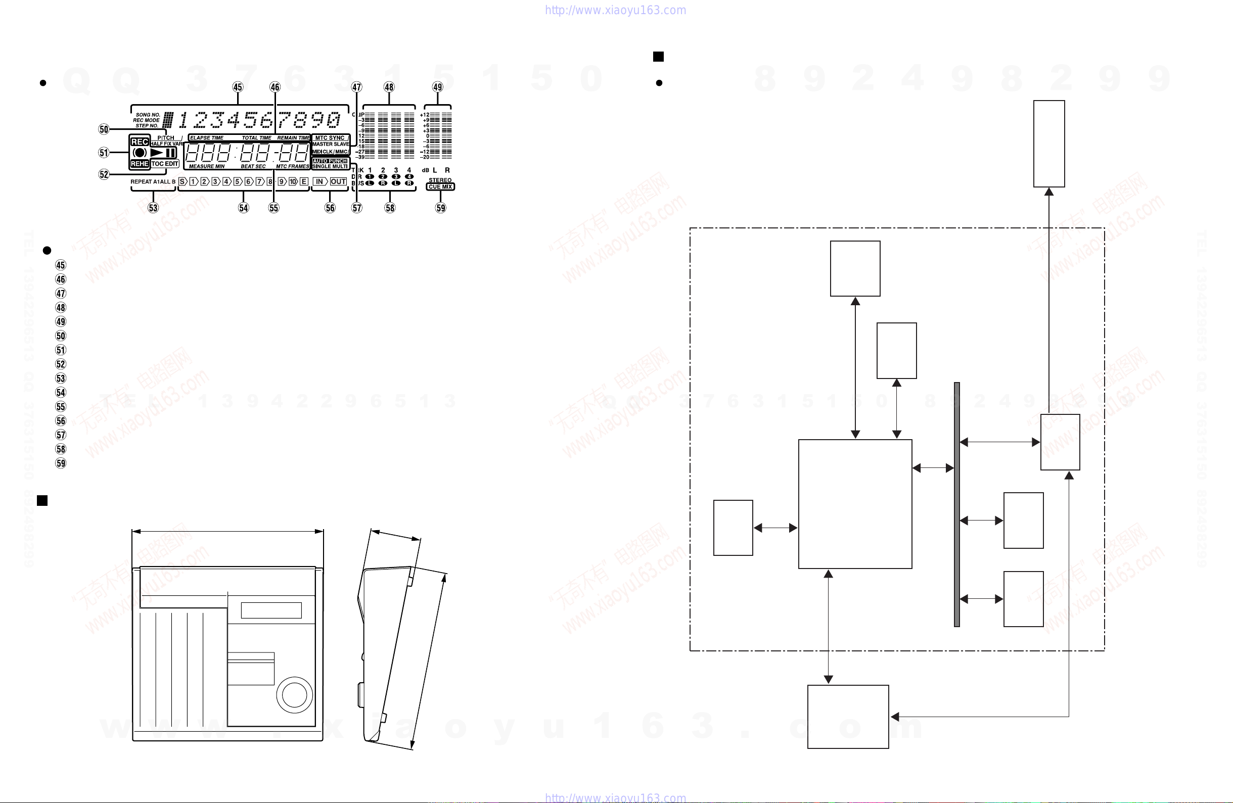
Display
Sampling Frequency: 44.1 kHz Compression: ATRAC
Frequency Response: 20 Hz–20 kHz, +1 dB, –3 dB
THD+N: Less than 0.02 % (1 kHz)
S/N: 96 dB typ.
4-track independent simultaneous record/play (Recording time: 37 min)
Dubbing with 4-track playback
Auto & Manual Punch In/Out (11.6 ms accuracy)
Four-track (37 min), Stereo (74 min), or Mono (148 min) record/play
Repeat play A-B, Single song, All song
Vari-pitch (+/-10 %)
Start and End point of Song Direct Time Locate
10 Marker locate points for each song Last Recording In/Out point
0.5x, 2x, 4x, 8x, 16x, 32x play speed
Disc Erase
Copy, Move, Divide, Combine, Renumber, Erase
Track Copy, Part Copy, Track Erase, Part Erase
Disc title, Song title
REC SELECT buttons 1–4, BUS button
Transport buttons: PLAY, STOP, PAUSE, REC, REHE, SONG SEARCH, EJECT
Mode buttons: AUTO PUNCH I/O, EDIT, UTILITY, ADJUST, PITCH, PEAK HOLD, DISPLAY, EXIT
CURSOR shuttle/DATA dial
Locate buttons: MARK, MARK SEARCH, LAST REC (IN/OUT), SEARCH, SET, REPEAT, A B
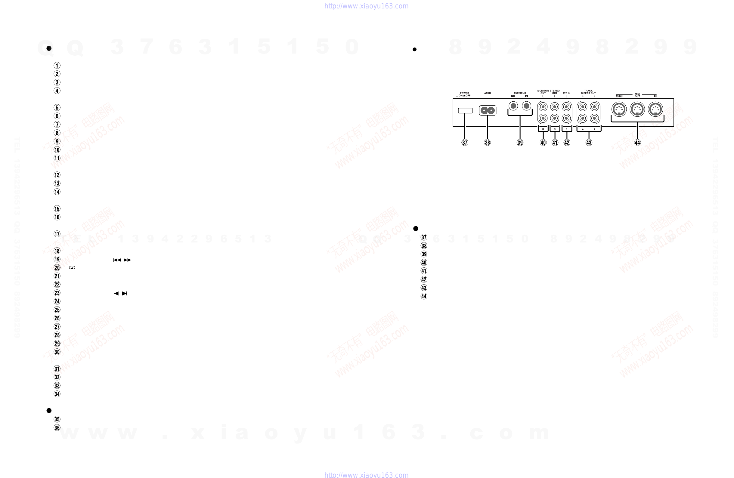
MIDI IN, OUT, THRU jacks
FLD (Fluorescent Display)
Inputs
Outputs
Frequency response
EQ
MASTER Channel Features
MIC/LINE IN (CH1, 2) Balanced phone jack x2 (–10 to –50 dB)
MIC/LINE IN (CH1, 2) Balanced XLR x2 (–10 to –50 dB)
MIC/LINE INPUT (CH3–4) Unbalanced phone jack x2 (–10 to –50 dB)
LINE INPUT (CH5–8) Unbalanced phone jack x4 (–10 dB)
INSERT IN/OUT (CH 1, 2) TRS phone jack x2 (–10 dB)
2 TR IN (L, R) Phono x2 (–10 dB)
TRACK DIRECT OUT (1–4) Phono x4(–10 dB)
STEREO OUT (L, R) Phono x2 (–10 dB)
MONITOR OUT (L, R) Phono x2 (–10 dB)
AUX SEND (1, 2) Phone jack x2 (–10 dB)
PHONES OUT Stereo phone jack (8–40 ohm)
20 Hz–20 kHz +1, –3 dB
3-band, +/-15 dB (LOW: 100 Hz shelving, MID: Peaking (2.5 kHz), HIGH: 10 kHz Shelving)
Stereo Fader (45 mm), Monitor Level control, Monitor Select buttons (2 TR IN, STEREO, CUE), CUE MIX TO
STEREO buttons
Power Requirements
Power Consumption
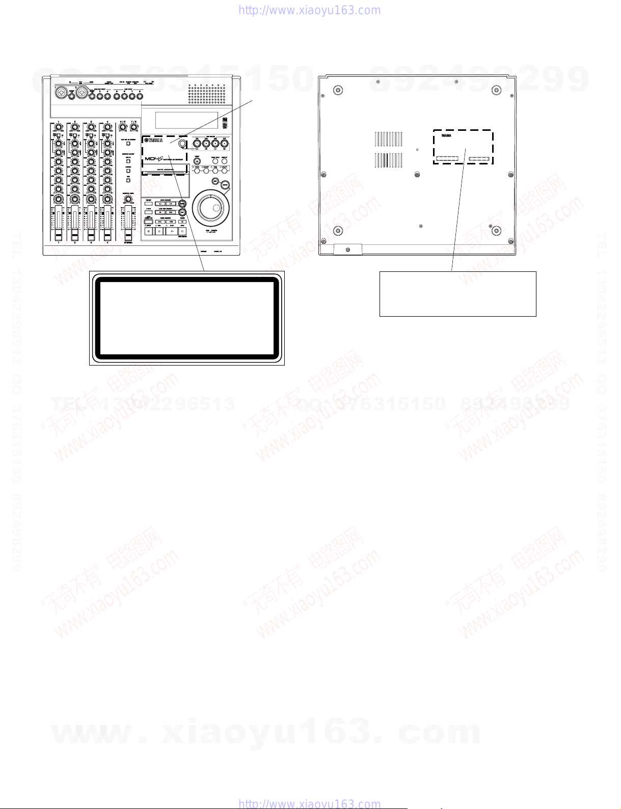
Dimensions (W x H x D)
Weight
Operating Conditions
Supplied Accessories
Optional Accessories
Output Level
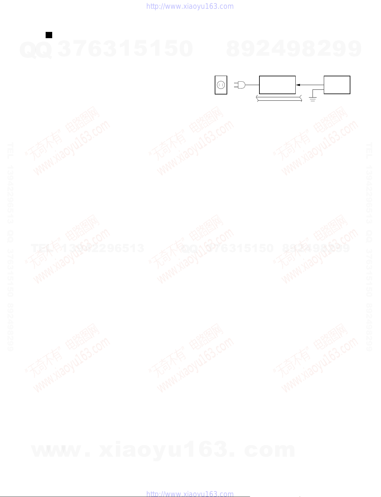
USA & Canada: 120 V/60 Hz, Others: 230 V/50 Hz
24 W
413 x 109.5 x 388 mm
5.2 kg
Temperature: 5 ˚C–35 ˚C (41 ˚F–95 ˚F), Humidity: 10 %–95 %
AC power cord, Owner’s Manual
FC5 Footswitch
Refer to the INSPECTION SPECIFICATION Section of this manual.
0 dB is referenced to 0.775 V r.m.s.