Zenisu Keisoku ZS-6123BP User manual

1
ZS-6123BP
GP-IB Adapter
User’s Manual
Ver. 1.0
Zip C de : 183-0027
2-13-37, H nmachi, Fuchu, T ky , Japan
TEL : +81-(0)42-368-2126 FAX : +81-(0)42-364-0067
URL http://www.zenisu.c .jp/

2
◆ Table f c ntents ◆
1.Outline ______________________________________________
3
2.Features _____________________________________________
3
3.Specificati n
_________________________________________________3
4.Appearance
__________________________________________________4
5.Signal and Switch
____________________________________________5
6.Input and Output data _________________________________
9
7.C nnecting table
_____________________________________________12
8.Warranty
_____________________________________________________14

3
1. Outline
ZS-6123BP is a GP-IB adapter with 8bit bidirecti nal data bus, 8bit address signal, and
ther signals.
ZS-6123BP can be easily c nnected between GP-IB bus signal and parallel signal such as
BCD.
M del GP-IB signal DATA signal Feature
ZS-6123BP GP-IB FC-50L It is able t c nnect GP-IB cable directly.
(Standard)
Type f c nnect r:
GP-IB :57LE-20240-77COD35G (DDK) : IEEE488 standard
FC-50L:FAP-5001-1202-0BF (Yamaichi) : L-angle 50-c nduct r flat cable
2. Features
(1) Timing and ther design is unnecessary.
(2) I/O data can be expanded up t 256 bytes.
(3) It can be expanded address by attaching an external address c unter.
3. Specificati ns
(1) This pr duct c mpliant with GP-IB interface standard (IEEE Std 488-1978)
(2) Interface functi n: SH1, AH1, T6L, 4SR1, RL1, PP0, DC1, DT1, C0
(3) Input perati n: It bec mes a talker and sends the utput data f the c nnected device t
the GP-IB. Signal level: TTL (fan-in = 1)
(4) Output perati n: It bec mes a listener and sends the input data f the GP-IB t the
c nnected device. Signal level: TTL (fan- ut = 10)
(5) P wer: +5V 0.5A
(6) Size (B ard): 114 x 155 x 30 (H) mm
(7) Weight: 150g r less
(8) Access ries
M del Name Type Quantity
ZS-6123BP
CN4 C nnect r FAS-5001-2101-0BF (Yamaichi) 1
CN7 Cable F r DC p wer, length 60cm 1

4
4. Appearance
M del
C nnect r
C1 CN4 CN3 CN7
ZS-6123BP GP-IB
FC-50L
B8B-XH-A B4B-XH-A

5
5. Signal and Switch
5.1 Input signal
Chart 5.1
N te) Output driver is equivalent t SN74LS541.

6
5.2 Signal descripti n
Input and utput in this manual are defined as sh wn ab ve.
Signal level is TTL except f r LED lighting.
D0 t D7 : Bidirecti nal bus f r I/O data.
A0 t A7 : Address bus, it dec des this signal and select the data f the c nnected circuit.
HS ENB : When this signal is set t High r Open with the data transfer enable signal,
the GP-IB handshake will be usable.
READ : It is a str be signal when reading data f the c nnecti n circuit t GP-IB.
WRITE : It is a write pulse signal when data fr m the GP-IB is utput t the c nnecti n
circuit.
STB1 t 8 : It is a status signal when SRQ ccurs. It will inf rm the SRQ t the GP-IB
c ntr ller.
GP-IB data
HS ENB
RD
Tf<2μs・
1
Th≧0
TRD
3.5μs≦TRD
2 3 4
WR(OUT) : It sends 1 pulse each time when it is received 1 byte f data fr m GP-IB.
The device latches the signal f data bus by “WR” signal and “AND” signal f
address signal.
GP-IB data
HS ENB
WR
1
Tdh > 0.25μs・
TWR≒1・
234
Tdf > 0.25μs・

7
DATA CR(IN) : When input is set t LOW level at talker, CR c de(ASCII) is sent ut.
DATA LF(IN) : When input is set t LOW level at talker, LF c de(ASCII) is sent ut.
DATA END(IN) : When input bec mes the HIGH level fr m the LOW level, talker
perati n is st p. It c nnects the gate signal f the last byte and EOI
is utput.
STB1 t STB8(IN) : It inputs the status data (negative l gic) t the c ntr ller when
SRQ ccurs.
*1: Set”1” when SRQ ccurs and bec me “0” after serial p lling.
REQUEST(IN) : At the rising f this signal, SRQ is generated.
SRQ : ZS-6123BP generates SRQ when REQUEST signal bec mes LOW level fr m
HIGH level. The c ntr ller perf rms serial p lling and checks the status byte.
After serial p lling is c mpleted, SRQ is reset.
TLK(OUT) : It bec mes LOW level when it is a talker.
LSN(OUT) : It bec mes LOW level when it is a listener.
BUSY(OUT) : It bec mes the LOW level at the falling f TLK utput signal and return t the
HIGH level at the falling f DATA END input signal. The BUSY signal is a
signal indicating that is being sent and is used f r data h ld signal f the
utput device.
GP-IBデータ
TLK
DATA END
BUSY
GP-IB DATA

8
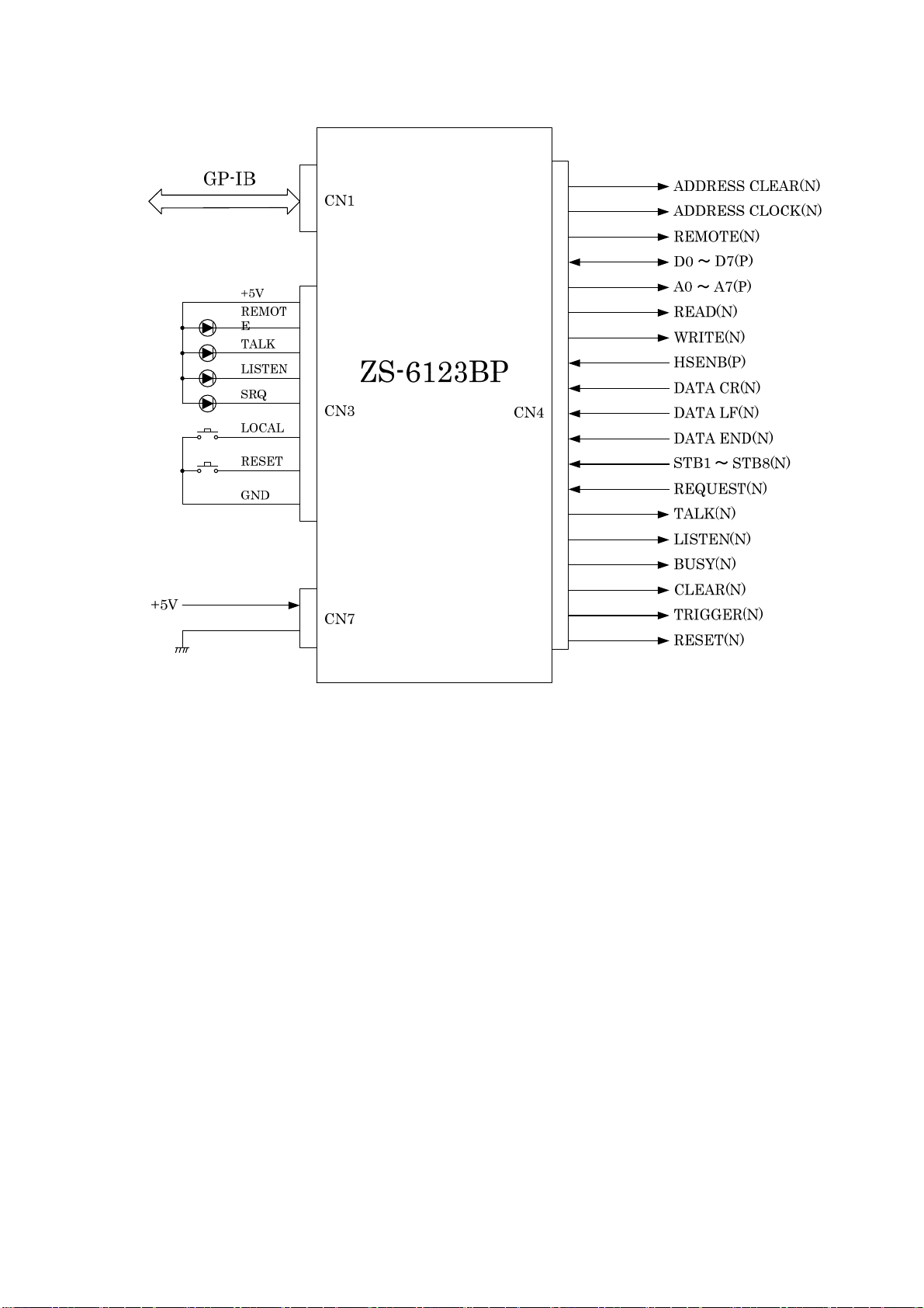
ADR-CR(OUT) : This signal clears the external address c unter.
ADR-CK(OUT) : This is cl ck signal f r external address c unter.
Please c unt up at the rising f this signal.
CLR(OUT) : When receiving SDC c mmand r DCL c mmand fr m the GP-IB c ntr ller,
it utputs 2µs negative pulse.
TRG(OUT) : When receiving GET c mmand fr m the GP-IB c ntr ller, it utputs 2µs
negative pulse.
RESET(OUT) : It utputs the LOW level signal when the p wer ON and reset signal is input.
RESET(IN) : Input f r external reset switch with pull-up resist r 10kΩ.
LED TLK(OUT) : Output f r the lighting the external LED with current limiting resist r 1kΩ.
It bec mes the LOW level at the talker.
LED LSN(OUT) : Output f r the lighting the external LED with current limiting resist r 1kΩ.
It bec mes the LOW level at the listener.
LED SRQ(OUT) : Output f r the lighting the external LED with current limiting resist r 1kΩ.
It bec mes the LOW level when SRQ is generated.
LED RMT(OUT) : Output f r the lighting the external LED with current limiting resist r 1kΩ.
It bec mes the LOW level when it is rem te perati n.
5.3 Address switch f GP-IB device
Set the GP-IB device address f the adapter.
1 2 3 4 5 6 7 8
O N
SW 1
A ddress C l ck select
1 t 5 : A ddress sw itch
6 t 8 : Internal cl ck frequ en cy
Initial setting : 10M H z
O N : "1"
O F F : "0"
# Frequency
0 78.125KHz
1 156.25KHz
2 312.5KHz
3 625KHz
4 1.25MHz
5 2.5MHz
6 5MHz
7 10MHz
N te) When using an external address switch, please turn ff all f this switch.
N te) Alth ugh the internal cl ck frequency is initialized t 10MHz. if it changes t l wer the
frequency, the utput pulse width such as TRG will be l nger.

9
6.Input / Output data
BCD and binary parallel signal equipment can be easily transfer data t PC via GP-IB
interface by adding address dec der, data latch circuit and gate circuit. It is necessary t use
the signal f ZS-6123BP data buses D0 t D7, address bus A0 t A7, WR, RD, ADR-CR,
ADR-LF in this case.
6.1 Example f r expanding utput data.
Chart 6.1
N te) In this circuit example, the number f utput data can be expanded up t 8 bytes by
adding a latch circuit LS273.

10
6.2 Example f r expanding input data
Chart 6.2
N te) In this circuit example, CR and LF are used as delimiters, and EOI is utput at the same
time as LF. The STROBE signal f r the final data is input t DATAEND. When the signal is
n t input, ZS-6123BP will c ntinue t send data t the GP-IB.

11
6.3 H w t generate delimiters
C nnect the dec der utput f the external additi nal circuit t DATACR, DATALF,
DATAEND acc rding t the c de f delimiter.
GP-IB DATA Last data LF
CR
1) When utputting EOI at the same time as CR, LF c de and LF, c nnect the str be bef re
the last data f data str be created by the dec der t DATACR and the str be f the last
data t DATALF and DATAEND. It is able t be sent t up t 254 bytes f data t GP-IB.
LFGP-IB data Last data CR
EOI
2) In case f EOI delimiter.
C nnect t the DATAEND f the last data f the data str be created by the dec der.
It is able t be sent up t 256 bytes f data t GP-IB.
GP-IB data Last data
EOI

12
7.C nnecting table
7.1 CN1 GP-IB c nnect r signal table
Signal Pin number Signal
DIO1 1 13 DIO5
DIO2 2 14 DIO6
DIO3 3 15 DIO7
DIO4 4 16 DIO8
EOI 5 17 REN
DAV 6 18 GND
NRFD 7 19 GND
NDAC 8 20 GND
IFC 9 21 GND
SRQ 10 22 GND
ATN 11 23 GND
SHILD 12 24 GND
57LE-20240-77COD35G(DDK)

13
7.2 CN4 C nnect r signal table
Signal Pin number Signal
RESERVE 1 2 GND
CLEAR *1 3 4 GND
RESET *2 5 6 GND
TRIGGER 7 8 GND
ADR-CR 9 10 GND
ADR-CK 11 12 GND
RD 13 14 GND
WR 15 16 GND
HSENB 17 18 GND
BUSY 19 20 GND
REQUEST 21 22 LISTEN
REMOTE 23 24 TALK
STB6 25 26 STB8
STB4 27 28 STB5
STB2 29 30 STB3
DATA-END 31 32 STB1
DATA-CR 33 34 DATA-LF
D6 35 36 D7
D4 37 38 D5
D2 39 40 D3
D0 41 42 D1
A6 43 44 A7
A4 45 46 A5
A2 47 48 A3
A0 49 50 A1
FC-50L:FAP-5001-1202-0BF (Yamaichi)
N te) +5V p wer supply is supplied fr m the CN7 c nnect r.
N te) Pin number 3 and 5 are reversed in the ZS-6123AP. Please be careful f r c nnecting
t the device.
*1 In the ZS-6123AP, the REST signal.
*2 In the ZS-6123AP, the CLEAR signal.

14
7.3 CN3 C nnect r signal
Please attach this c nnect r when attaching m nit r LED and switch t the utside.
Pin number Signal
1 +5V
2 REMOTE LED
3 SRQ LED
4 TALK LED
5 LISTEN LED
6 LOCAL SW
7 RESET SW
8 GND
B8B-XH-A (JST)
7.4 CN7 C nnect r signal
Pin number Signal
1 +5V
2 +5V
3 GND
4 GND
B4B-XH-A (JST)
8. Warranty
If it fails during n rmal use, we will repair it free f charge as described in this warranty
as bel w.
1) During the warranty peri d which is ne year fr m the data f purchase, we will
repair it free f charge in case f malfuncti n in acc rdance with instructi n manual.
2) It will be charged f r extra in the f ll wing case, even during warranty peri d.
Inc rrect usage f failure r damage caused by carelessness,
Failure r damage caused by impr per repair r rem deling.
Failure r damage caused by external fact rs such as fire, earthquake, ther
natural disasters, abn rmal v ltage and s n.
Change f p wer supply and v ltage.
This warranty pr visi n is effective nly in Japan.
Table of contents
Other Zenisu Keisoku Adapter manuals

Zenisu Keisoku
Zenisu Keisoku ZS-6822A Series User manual

Zenisu Keisoku
Zenisu Keisoku ZS-6144AF User manual

Zenisu Keisoku
Zenisu Keisoku ZS-6225 Series User manual

Zenisu Keisoku
Zenisu Keisoku ZS-6216E User manual

Zenisu Keisoku
Zenisu Keisoku ZS-6228-8N Series User manual

Zenisu Keisoku
Zenisu Keisoku ZS-6222A Series User manual

Zenisu Keisoku
Zenisu Keisoku ZS-6222 Series User manual

Zenisu Keisoku
Zenisu Keisoku ZS-6822 User manual