Zenith Z-100 PC series User manual
SERVICE MODULE
Power Supply
Z-100 PC Series Computers
585-60-01 860-45
aNI'N
data
~.
systems

The
purpose of this page is to make sure that all service bulletins are
entered in this manual. When a service bulletin is received, annotate the
manual and list the information
in
the record below.
Record
of
Service
Bulletins
SERVICE DATE CHANGED PURPOSE OF SERVICE INITIALS
BULLETIN OF PAGE(S) BULLETIN
NUMBER ISSUE
)
LIMITED RIGHTS LEGEND
Contractor is Zenith Data Systems Corporation of
St.
Joseph, Michigan 49085. The entire
document is subjectto Umited Rights data provisions.
Copyright ©1984 Zenith Data Systems Corporation, all rights reserved.
Printed in the United States of America
Zenith Data Systems Corporation
St. Joseph, Michigan 49085
Contents
Record
of Service Bulletins
II
Figures
III
Abbreviations
v
Chapter
1 Introduction
and
Specifications
Introduction . . . . . . . . . . . . . . . . . . . . . . . . . . . . . . . . . . . . . . . . . . . . . . . . . . . .
1.1
Specifications . . . . . . . . . . . . . . . . . . . . . . . . . . . . . . . . . . . . . . . . . . . . . . . . . .
1.1
Chapter
2 Configuration
Chapter
3 Theory of Operation
Introduction
....................................................
3.1
Outputs
.......................................................
3.1
Power Supply Good (PSG) Signal
...............................
3.3
Operation at
No
Load
.........................................
3.3
Chapter
4 Troubleshooting
Figures
2.1
Power Supply Rear View
....................................
2.1
3.1
Power Supply Output
.......................................
3.2
4.1
Power Supply Connectors
...................................
4.1
Abbreviations
CSA
Canadian Standards Association
FCC
Federal Communications Commission
KHz
Kilohertz
ms
millisecond
mV
millivolt
PSG
Power Supply Good
TTL
Transistor-Transistor Logic
UL
Underwriters Laboratories
VAC
Voltage Alternating Current
VDC
Voltage Direct Current
VDE
German Engineers Association
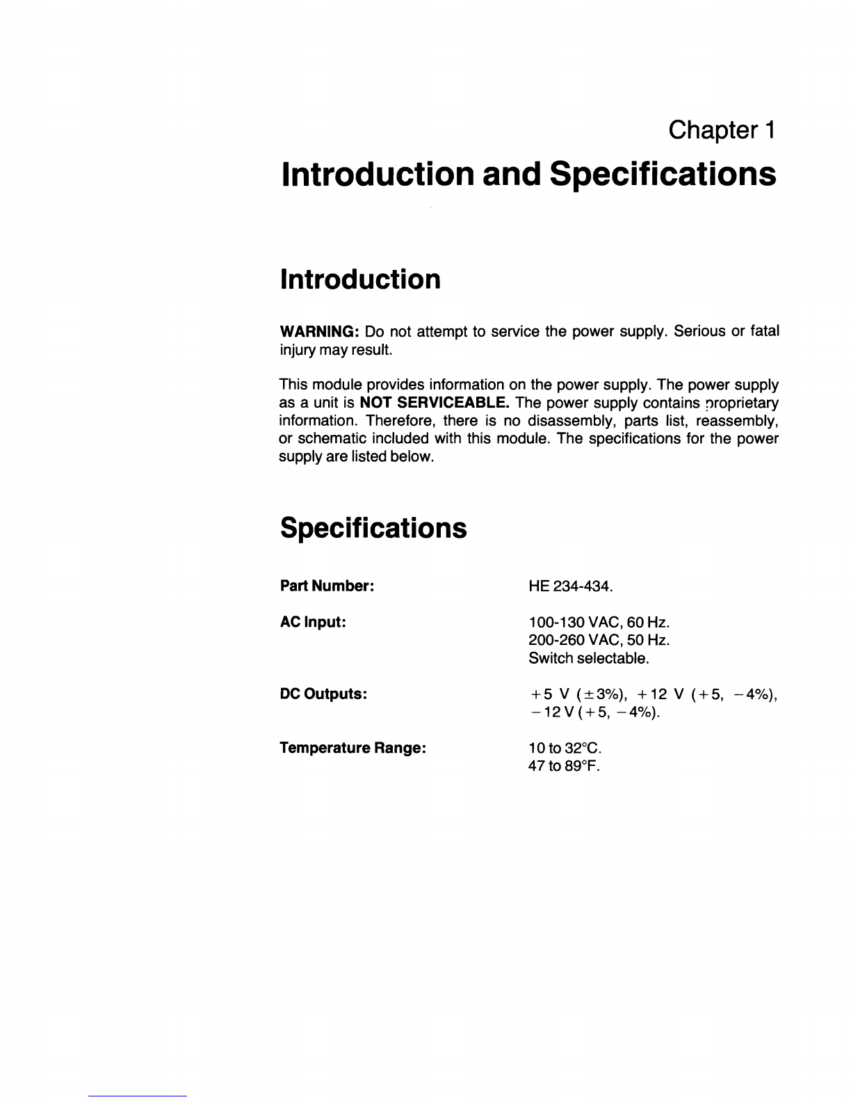
Chapter 1
Introduction and Specifications
Introduction
WARNING: Do not attempt to service the power supply. Serious or fatal
injury may result.
This module provides information on the power supply. The power supply
as a unit
is
NOT SERVICEABLE. The power supply contains
~roprietary
information. Therefore, there is no disassembly, parts list, reassembly,
or schematic included with this module. The specifications for the power
supply are listed below.
Specifications
Part Number: HE 234-434.
AC
Input: 100-130 VAG, 60 Hz.
200-260 VAG, 50 Hz.
Switch selectable.
DC
Outputs:
+5
V
(±3%),
+12
V
(+5,
-4%),
-12
V
(+5,
-4%).
Temperature Range: 10to 32°G.
47 to 89°F.

Chapter 2
Configuration
Refer
to
Figure
2.1
while reading the following.
The voltage switch at the rear of the computer is located through the
small window
on
the power supply that
is
covered with plastic. The voltage
switch
is
normally set for 115
VAC.
If
this computer
is
to
be
operated
on
240 VAC line voltage, use a small-bladed screwdriver and break the
plastic window over the 115 VAC position of the switch. Then slide the
switch so that 240 VAC
is
visible
on
the switch. Connect the appropriate
line cord.
@l')
~
~
~
®
~
,,
"
@.
~
0 0
§o
g~~~
§
~
@
[ _c.,,,,;,:;
:'~:;':::.J
;.'
1
© "
, ,
"
,,
"
~
®
rft
00
, ,
, ,
00
,,
,,
"
~
@
[U
00
0 0
go
@
~
~
®
rf.;-
,'
00
og
0,
0 0
0 0
00
0 0
~
@
@
~
00
\
\
~
@
'--
'--
I....-
--
l....-
I--
@
-/
POWER
SUPPLY
Figure 2.1. PowerSupply Rear View
Chapter 3
Theory of Operation
Introduction
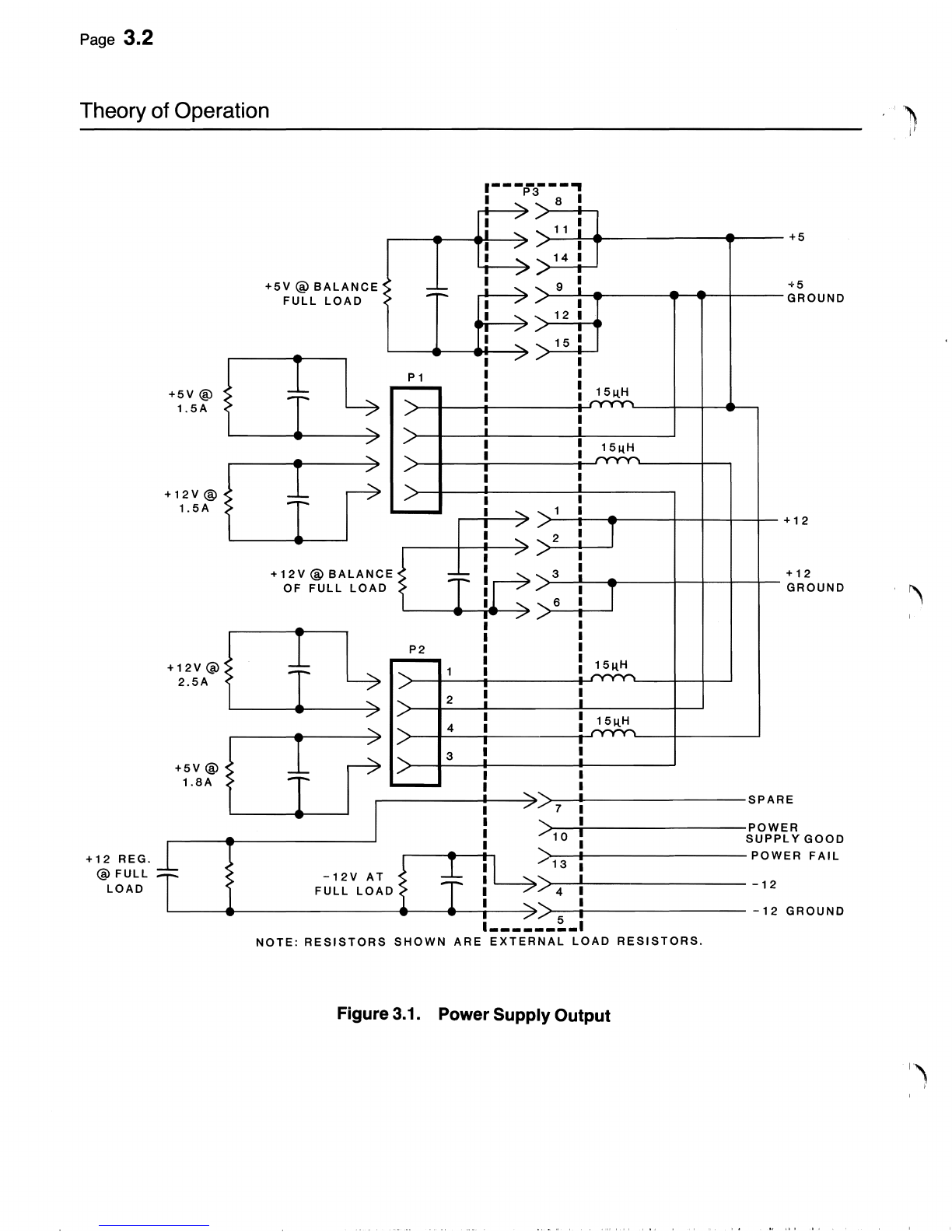
Refer to Figure
3.1
while reading the following.
The
power supply provides regulated voltages used by the various compo-
nents within the Z-100
PC
Series Computers. The power supply
is
located
toward the rear and to the right of the chassis, and uses a quasi square
wave switching regulator to produce three regulated output voltages. This
unit complies with FCC, VDE, CSA, and UL regulations.
Outputs
All
outputs from the precision-regulated power supply are electrically iso-
lated from the main voltage and share a common ground, which is the
chassis of the power supply.
The
voltages output to disk drive connectors
P1
and
P2
have special
requirements for output ripple frequency components
in
the frequency
range
of 60 to 120 KHz. To obtain these low levels, a low pass filter
is
added to the regular output leads of
P1
and
P2.
The output ripple
is
measured with an oscilloscope with a bandwidth of 3 KHz. Component
frequency of the output ripple of the 5-volt or 12-volt outputs should NOT
exceed 2 mV peak between the frequencies of 60 KHz to 120 KHz. Con-
nector P3 supplies the output voltages to the backplane board.
Page 3.2
Theory
of
Operation
L-----
....
------------------
- 12 GR0 UND
--
______
1
NOTE:
RESISTORS
SHOWN
ARE
EXTERNAL
LOAD
RESISTORS.
Figure 3.1. Power Supply Output
+5V
@
1.5A
+12V
@
1.5A
+12V
@
2.5A
+5V@
1.8A
+12
REG.
@
FULL
LOAD
1-------
...
P3
8 I
+5
+5V
@
BALANCE
+5
FULL
LOAD
GROUND
15
I
I
P1 I
I
I
151lH
151lH
+12
+
12V
@
BALANCE
+12
OF
FULL
LOAD
GROUND
~
r---------~~--~)~7--~----------------SPARE
)
~--~-----------------POWER
10
SUPPLY
GOOD
)>-1-3---,1f-----------------
POW
ER FAIL
-12V
AT
)>-4--!--------
- 12
FULL
LOAD
......
-----t~-i---~>~-5-i:-----------------
Page
3.3
Theory of Operation
Power Supply Good (PSG) Signal
The
PSG
logic signal
is
an
open collector TTL-compatible output which
is
used by external circuits
to
determine if the output voltages are valid
and
within specification. Upon power
up,
PSG
shall remain high until all
the
DC
output voltages stay within specification for a minimum of
70
to
130
ms,
after which time
PSG
will go low.
If
any voltage
is
not within
this
normal limit plus 1% of nominal voltage (refer to Specifications),
PSG
will
go
high.
PSG
will not return
to
a low condition until outputs have
met
the same conditions
as
those required at initial power application.
Operation at No Load
The
power supply
is
capable of operating under the adverse condition
of
no
load without damage. If the power supply shuts down, it will require
a manual reset by turning the power supply
off,
waiting 5 seconds, and
then
turning it back
on.
The output voltage may seek a value between
ground and 50% over nominal. Output voltages will not exceed the peak
rating
ofthe output circuit components.

Chapter 4
Troubleshooting
Refer to Figure
4.1
while reading the following.
Measure the power supply outputs with the disk drive connectors discon-
nected, and connector
P3
connected to the backplane board. Measure
the voltages at the test points on the backplane board, and refer to Figure
4.1
for the power supply voltages.
Measure the ripple voltage with
an
oscilloscope. If the power supply volt-
ages
are normal, measure the voltage with the disk drives connected.
This will indicate if the circuit cards or disk drives are loading down the
power supply.
WARNING: The load resistors listed below generate heat. Use caution
to avoid burns.
NOTE: Voltages may not be within tolerance. The correct loads for the
output voltages are: +5
Vat
4 Amps (1.25-ohm resistor rated at 20 watts
or greater), +12 V at
tAmp
(12-ohm resistor rated at 12 watts or greater),
and
-12
V at 250
rnA
(50-ohm resistor rated at 3.5 watts orgreater).
ROW
1
ROW
2
ROW
3
PIN
ORG+12V
ORG+12V
BlK
GND
WHT-12V
BlK
GND
BlK
GND
ORG+12V
RED
+5V
BlK
GND
VEL
PSG
RED
+5V
BlK
GND
BlU
PFL
RED
+5V
BlK
GND
ORG
Bl~
P2
BL~I~"'V
RED~j:
m
ROW
3
ROW
2
ROW
1
TO
DISK
DRIVE
Figure 4.1. Power Supply Connectors
SERVICE MODULE
Backplane Board
Z-100 PC Series Computers
585-64-02 860-45
aNI'.
data
~
systems

The
purpose of this page
is
to
make sure that all service bulletins are
entered
in
this manual. When a service bulletin
is
received, annotate the
manual
and list the information
in
the record below.
Record
of
Service
Bulletins
SERVICE DATE CHANGED PURPOSE
OF
SERVICE
BULLETIN OF PAGE(S) BULLETIN
NUMBER ISSUE
INITIALS
LIMITED RIGHTS LEGEND
Contractor is Zenith Data Systems Corporation of St. Joseph, Michigan 49085. The entire
document issubjectto Umited Rightsdataprovisions.
Copyright ©1984Zenith DataSystems Corporation, all rights reserved.
Printed in the United States
of
America
Zenith Data Systems Corporation
St. Joseph, Michigan 49085
Contents
Record
of Service Bulletins
II
Figures Iv
Tables Iv
Abbreviations v
Chapter
1 Introduction
and
Specifications
Introduction . . . . . . . . . . . . . . . . . . . . . . . . . . . . . . . . . . . . . . . . . . . . . . . . . . . .
1.1
Diagnostics . . . . . . . . . . . . . . . . . . . . . . . . . . . . . . . . . . . . . . . . . . . . . . . . . . . .
1.1
- 5 Volt Regulator
..............................................
1.1
Signal Bus
..............................
. . . . . . . . . . . . . . . . . . . . . . 1.2
Chapter
2 Theory of Operation
Power Connector
...............................................
2.1
-5
Volt Regulator
..............................................
2.2
Diagnostic LEDs
...............................................
2.2
Backplane I/O Connectors
.......................................
2.2
Chapter
3 Detailed Circuit Description
Power Distribution
...............................................
3.1
- 5 VDC Regulation
............................................
3.1
Diagnostic Circuitry
..............................................
3.2
Signal
Bus
....................................................
3.2
Chapter 4 Troubleshooting
General Troubleshooting
.........................................
4.1
DC
Voltages and Diagnostics
....................................
4.1
DC
Voltage Checks
...........................................
4.1
Backplane Connector Fault Isolation
...............................
4.3
Chapter
5 Parts List
Introduction
....................................................
5.1
Component Parts List
...........................................
5.1
Semiconductor Identification Index
.................................
5.2
Schematic . . . . . . . . . . . . . . . . . . . . . . . . . . . . . . . . . . . . . . . . . . . . . . . . . . Fold-in
Page
iv
Contents
Figures
2.1
Backplane Board Block Diagram
..............................
2.1
5.1
Backplane Board Component Layout
..........................
5.3
Tables
3.1
I/O
Bus Signal Names
......................................
3.3

Abbreviations
ClK
Clock
CPU
Central Processing Unit
DC
Direct Current
DMA
Direct Memory Access
GND
Ground
liD Input/Output
lED
Light-Emitting Diode
mA
Milliamperes
MHz
Megahertz
NMI
Non-Masked Interrupt
ns
nanosecond
PSG
Power Supply Good
ROM
Read-Only Memory
VDC
Volts DirectCurrent
Chapter 1
Introduction and Specifications
Introduction
The backplane board in the Z-100 PC Series Computer contains five sup-
ply voltage diagnostic LEDs, a - 5 VDC regulator, and the eight
IBM®-
compatible bus connectors,
P101
through P108, into which the remainder
of the computer's cards are inserted for intersystem communication. A
power supply interface connector,
P11
0,
and a +12 VDC connector, P109,
also are contained on this board. P109 supplies +12 VDC to an internal
video monitoron some models.
Diagnostics
The
LEDs on the backplane board aid the user in determining whether
or not a fault lies in the DC power generation circuits. The five LEDs
on
this board indicate the overall integrity of the power supply, and the
presence or absence of the four individual operating supply voltages: +12
VDC,
-12
VDC, +5 VDC, and - 5 VDC.
-5 Volt Regulator
The
only supply voltage actually generated on this board is the - 5 VDC.
The
specifications forthis supply are as follows:
•
Input:
-7.3 to -25 VDC, filtered by 2.2
JLF.
•
Output:
-4.8to
-5.2
VDC, at 100
rnA,
filtered by 47
JLF.
• Load: 1
rnA
to 100
rnA,
short-circuit protected.
•
Ambient
Temperature: 0 to +70°C.
32
to 158°F.
"'IBM
is
a
registered
trademark of International
Business
Machines
Corporation.

Page
1.2
Introduction and Specifications
Signal Bus
The
eight-connector array on this board is basically
an
input/output (I/O)
extension
of
the microprocessor bus. The bus interface
is
implemented
via a 62-pin edge connector on the card or device which plugs into one
of
the eight backplane sockets. The bus supplies the following:
• Eight bits ofbidirectional data;
• Twenty address lines to access up to 1 megabyte of memory. The
maximum user memory is 640K of 64K devices, or 76aK using 256K
devices;
• Six levels ofinterrupt;
• Control lines for memory and I/O read and write;
• Clock and timing control lines;
• A channel check line for device error reporting or parity error reporting
by existing and add-on memory. A non-masked interrupt (NMI) is
supplied to the central processing unit (CPU) when this line is active;
• Operating power consisting of + and - 5 VDC, + and -12 VDC,
and ground;
•
An
I/O CH RDY line for use by slowacting peripherals;
• Capability ofaddressing up to 64K I/O ports;
A complete listing of the signal names and their functions
is
presented
in
the "Detailed Circuit Description," Chapter
3.
Chapter
2
Theory of Operation
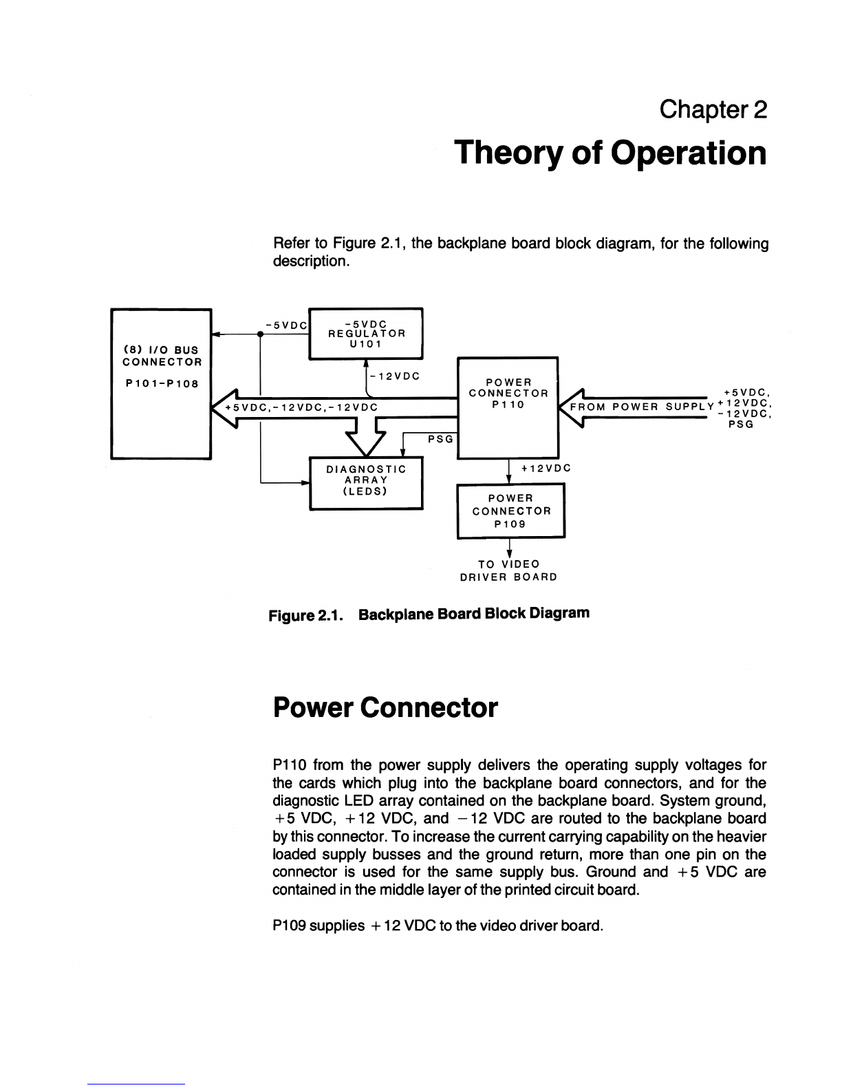
Refer to Figure 2.1, the backplane board block diagram, for the following
description.
-5VDC
-5VDC
REGULATOR
U101
(8)
1/0
BUS
CONNECTOR
~
-12VDC
P101-P108
POWER
CONNECTOR
+5VDC.
P1
10
y+
12VDC.
~VDC'-
12VDC,-'
'VDC
f:6'OM
POWER
SUPPL
-12VDC.
0~
PSG
PSG
DIAGNOSTIC +
+12VDC
ARRAY
(LEDS)
POWER
CONNECTOR
P109
TO VIDEO
•
DRIVER BOARD
Figure 2.1. Backplane Board Block Diagram
Power
Connector
P110
from the power supply delivers the operating supply voltages for
the
cards which plug into the backplane board connectors, and for the
diagnostic LED array contained
on
the backplane board. System ground,
+5 VDC, +12 VDC, and -12 VDC are routed to the backplane board
by
this connector. To increase the currentcarrying capability on the heavier
loaded supply busses and the ground return, more than one pin on the
connector
is
used for the same supply bus. Ground and +5 VDC are
contained
in
the middle layerofthe printed circuit board.
P109
supplies +12 VDC to the video driver board.

Page
2.2
Theory
of
Operation
-5 Volt Regulator
The
- 5 volt supply is derived from
-12
VDC from the power supply,
which
is applied to a solid-state voltage regulator, U101. The - 5 VDC
is
then applied to the parallel bus connectors, and
to
its respective diagnos-
tic
LED
circuit.
Diagnostic LEOs
Five
green light-emitting diodes (LEDs) are incorporated to indicate the
power supply is good, and the presence or absence of +5 VDC, - 5
VDC,
+12 VDC, and -12 VDC. Suitable current-limiting resistors are
connected inline with the LEDs to provide the appropriate operating volt-
age
and current to the devices. The LEDs are on (lit) when the parameter
associated with a device is at or near its stated value, and off when the
associated parameter is deficient.
Backplane 1/0 Connectors
Eight 62-pin edge-type socket connectors are provided by the backplane
board
to interconnect the CPU card, the memory card, the video card,
and
the disk controller card with the appropriate edge connector, as well
as
any other cards which may
be
added for system enhancement or ex-
pansion. The optional connectors are identical and are wired in parallel
so
that, functionally, any card may
be
inserted at any connector location.
Chapter
3
Detailed Circuit Description
Refer
to the backplane board schematicfor the following circuit description.
Power Distribution
P110,
the backplane power connector, connects + 5
VDC,
+ 12
VDC,
-
12
VDC,
the power supply good (PSG) signal, and ground to the back-
plane
board. Ground
is
connected
to
pins
3,
5,
6,
9,
12,
and
15.
+ 5
VDC
comes
in
on
pins
8,
11,
and
14.
-12
VDC
appears
on
pin
4.
+
12
VDC
is
applied to pins 1 and
2.
The
PSG
signal
is
on pin
10.
Pins 7
and
13 are not used.
+5
VDC,
+
12
VDC,
and
-12
VDC are
fed
through to
B3,
B9,
and
B7,
respectively,
on
the parallel signal bus connectors,
P101
through P108,
and
also are applied
to
their respective
LEOs.
-12
VDC
also is fed
to
the
input, pin I of
U1
01,
the - 5
VDC
regulator. Ground (GND) is routed
to
the
signal bus, pins
B1,
B10,
and
B31.
The
PSG
signal is connected
to
the cathode of 0104, the
PSG
LED.
-5 VDC Regulation
U101,
the
-5
volt regulator, accepts the
-12
VDC
on its input, drops
and
regulates
it,
and sends the - 5 VDC output,
pin
0,
to bus
pin
B5,
and
to
R1
01, the dropping resistor for the - 5 volt
LED.
The G pin of
U101
connects
to
system ground to serve
as
a return path for the regulator
circuit. C119 and C117 filter and decouple the
-12
VDC
input. C118
filters the - 5 VDC outputto reduce the ripple to
an
acceptable level.
Table of contents
Popular Power Supply manuals by other brands

VOSS.PET fenci
VOSS.PET fenci M03 operating instructions

Whelen Engineering Company
Whelen Engineering Company ISP18824 installation guide

RKI Instruments
RKI Instruments 49-0121-10 Operator's manual

teko
teko Astra-712/0 operating manual

TEXIO
TEXIO PSW Series instruction manual

MATRIX TECHNOLOGY
MATRIX TECHNOLOGY MPS-3063S user manual


