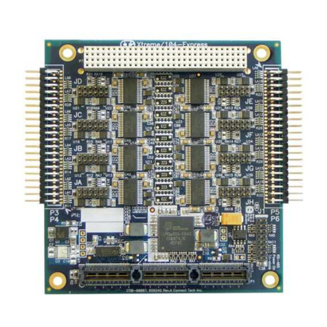
Acces I/O products mPCIE-ADIO16-8F Series User manual

ACCES I/O Products, Inc. MADE IN THE USA mPCIe-ADIO16-8F Family Manual
2Rev B1f
CHAPTER 1: QUICK START
It is recommended that you install the software package before
installing the PCI Express Mini (mPCIe) or M.2 card in your
computer. You can install the software1using our stand-alone
installer downloaded from the website.
Run the installer you downloaded and follow the prompts to install
the software for your device.
Please note: during the installation you may be prompted regarding
the installation of non-WHQL-certified drivers; please carefully
confirm the digitally signed source of the drivers and accept the
installation.
Once the software has been installed, shut down your system and
carefully install the mPCIe card.
Re-start your system. Once the computer finishes booting, your
new I/O should already be installed and ready for use; you can
confirm this by launching Device Manager and looking under the
“Data Acquisition” section. If, for any reason, the device displays a
warning triangle, right-click and select “Update Driver”.
1In Linux or OSX please refer to the instructions in those directories.
CHAPTER 2: INTRODUCTION
This manual is applicable to both the PCI Express Mini Card (mPCIe)
and M.2 card versions of this product. The registers, I/O and
performance specifications are the same.
•PCI Express Mini Card (mPCIe) type F1 or M.2 type 2280/2260,
with latching I/O connector
•16-bit, Bipolar, Differential, A/D converter
•Software selectable as 8 Single-Ended (Pseudo-differential) or 4
Differential Inputs
•7 channel-by-channel programmable differential input ranges
from ±0.3125V up to ±12V (48Vp-p)
•Sustained sampling rates up to 1MHz
•A/D starts via software, external input, or periodic timer
•A/D “Scan Start” mode optimizes inter-channel timing
•High impedance, 8-channel input: 1 MΩ
•32k FIFO plus DMA for efficient, robust data streaming
•Four 16-bit analog outputs
•5 per-channel programmable ranges: 0V to 5V, 0V to 10V,
±2.5V, ±5V, ±10V
•Outputs Drive ±10mA Guaranteed
•16 Digital I/O; 8 individually configurable for input/output
•Onboard Watchdog with status output
•RoHS compliant standard
CHAPTER 3: HARDWARE
This manual applies to the following models:
VENDEV
mPCIe-ADIO16-8F
mPCIe, A/D 16-bit, 1MHZ, 4 D/A
494F:C0EC
mPCIe-ADIO16-8A
mPCIe, A/D 16-bit, 500KHZ, 4 D/A
494F:C0ED
mPCIe-ADIO16-8E
mPCIe, A/D 16-bit, 250KHz, 4 D/A
494F:C0EE
mPCIe-ADI16-8F
mPCIe, A/D 16-bit, 1MHZ
494F:80EC
mPCIe-ADI16-8A
mPCIe, A/D 16-bit, 500KHZ
494F:80ED
mPCIe-ADI16-8E
mPCIe, A/D 16-bit, 250KHz
494F:80EE
mPCIe-ADIO12-8A
mPCIe, A/D 12-bit, 500KHZ, 4 D/A
494F:C05C
mPCIe-ADIO12-8
mPCIe, A/D 12-bit, 250KHz, 4 D/A
494F:C05D
mPCIe-ADIO12-8E
mPCIe, A/D 12-bit, 100KHz, 4 D/A
494F:C05E
mPCIe-ADI12-8A
mPCIe, A/D 12-bit, 500KHZ
494F:C05C
mPCIe-ADI12-8
mPCIe, A/D 12-bit, 250KHz
494F:C05D
mPCIe-ADI12-8E
mPCIe, A/D 12-bit, 100KHz
494F:C05E
These models are full-length “F1” mPCIe devices (30 × 50.95 mm).
All units are RoHS compliant.
INCLUDED IN YOUR PACKAGE
•mPCIe-ADIO card
Available accessories include:
CAB-mPCIe-ADIO
9 inch panel-mount DB37M twisted pair cable
assembly
ADAP37F-MINI
Direct plug-on terminal board mates with
DB37M on CAB-mPCIe-ADIO
LF-BRK-P9259-37
Mounting bracket for DB37M on CAB-mPCIe-
ADIO
mPCIe-HDW-KIT2
Mounting hardware for 2mm
mPCIe-HDW-KIT2.5
Mounting hardware for 2.5mm
Contact the factory for information regarding additional accessories,
options, and specials that may be available to best fit your specific
application requirements, such as Industrial Temperature (-40°C to
85°C).
CHAPTER 4: CONFIGURATION SETTINGS
All configuration of this device is performed through software; there
are no jumpers or switches to set.

ACCES I/O Products, Inc. MADE IN THE USA mPCIe-ADIO16-16F Family Manual
3 Rev B1f
CHAPTER 5: PC INTERFACE
This product interfaces with a PC using a PCI Express Mini Card
(mPCIe) connection; a small-form-factor, high-performance, rugged
peripheral interconnect technology first introduced for use in
laptops and other portable computers.
mPCIe’s small size and powerful performance, combined with
perfect software compatibility with PCI and PCIe peripheral designs,
have led to its recent adoption as a go-to standard for embedded
Data Acquisition and Control, and many other applications.
Although mPCIe is a broadly-adopted industry standard, the actual
connection to the computer shares a specification with mSATA:
both mSATA and mPCIe use the same edge-connector. In fact, well-
designed PCs can automatically detect and configure their onboard
connectors to work with either mPCIe or mSATA devices –and,
according to the standards for mPCIe and mSATA they are supposed
to do so! However, some PC manufacturers ship computers that
only support mSATA devices. Please confirm in your PC
documentation that your edge-connector is actually PCI Express
Mini Card compliant before installing this, or any, mPCIe card.
Damage might occur if you install an mPCIe device into a computer
that only supports mSATA.
mPCIe defines mounting holes for securing the otherwise loose end
of the card, so it is impossible for these cards to wiggle or flap
themselves loose (which was a recurring problem with the older PCI
Mini devices). Eliminating this concern for PCI Express Mini Cards is
a major reason this standard has seen rapid adoption by the Data
Acquisition and Control industry. Unfortunately, a variety of
mounting standoff lengths exist; ACCES offers stand-off kits in both
2mm and 2.5mm sizes. Some computers may provide stand-offs.
Please consult your computer manufacturer if it requires a different
size.
The mPCIe standard, like its PCI Mini Card predecessor, was
designed assuming use primarily in Laptop or Notebook and similar
devices, where physical dimension is often the paramount design
constraint. In Data Acquisition and Control applications low-weight
and vibration tolerance tend to be of more concern.
CHAPTER 6: I/O INTERFACE
Most customers will use the optional cable assembly CAB-mPCIe-
ADIOs D-Sub Miniature 37-pin Male connector.
For Singled-Ended analog inputs connect GND to ADC COMMON.
CAB-mPCIe-DB37M Male 37-Pin Pinout
S.E. Signal (Diff)
Pin
Assignment
GND
1
20
GND
ADC COMMON
2
21
ADC Ch 0 (Ch 0+)
ADC Ch 1 (Ch 0-)
3
22
ADC Ch 2 (Ch 2+)
ADC Ch 3 (Ch 2-)
4
23
ADC Ch 4 (Ch 4+)
ADC Ch 5 (Ch 4-)
5
24
ADC Ch 6 (Ch 6+)
ADC Ch 7 (Ch 6-)
6
25
GND
GND
7
26
DAC 0
DAC 1
8
27
DAC 2
DAC 3
9
28
GND
GND
10
29
VCCio1
DIO 15
11
30
DIO 14
DIO 13
12
31
DIO 12
DIO 11
13
32
DIO 10
DIO 9
14
33
DIO 8
DIO 7
15
34
DIO 6
DIO 5
16
35
DIO 4
DIO 3
17
36
DIO 2
DIO 1
18
37
DIO 0
Digital GND
19
1: VCCio pin outputs fused 3.3VDC on COTS models. -TTL MCOTS
option converts VCCio into a user input between 1.65VDC and
5.5VDC
For customers needing deeper integration the on-card connector is
a 40-pin latching Molex 501190-4017 connector. The mating
connector is the Molex 501189-4010.
40-Pin latching wire-to-board connector
S.E. Signal (Diff)
Pin
Assignment
ADC Ch 0 (Ch 0+)
1
2
ADC Ch 4 (Ch 4+)
ADC Ch 1 (Ch 0-)
3
4
ADC Ch 5 (Ch 4-)
GND
5
6
GND
ADC Ch 2 (Ch 2+)
7
8
ADC Ch 6 (Ch 6+)
ADC Ch 3 (Ch 2-)
9
10
ADC Ch 7 (Ch 6-)
GND
11
12
GND
COMMON
13
14
GND
GND
15
16
GND
DAC0
17
18
DAC1
DAC2
19
20
DAC3
GND
21
22
GND
VCCio1
23
24
Digital GND
DIO8
25
26
DIO0
DIO9
27
28
DIO1
DIO10
29
30
DIO2
DIO11
31
32
DIO3
DIO12
33
34
DIO4
DIO13
35
36
DIO5
DIO14
37
38
DIO6
DIO15
39
40
DIO7
Alternately, custom hardware cables and/or interfaces can be
produced to fit your specific application requirement.

ACCES I/O Products, Inc. MADE IN THE USA mPCIe-ADIO16-8F Family Manual
4Rev B1f
CHAPTER 7: SOFTWARE INTERFACE
How to use
The ADAS3022 is a flexible data acquisition system-on-chip that has numerous features and modes of operation, and additional modes and features are added by our advanced FPGA
design.
This flexibility can seem overwhelming, but we’ve designed our AIOAIO.dll API to make using this ADC simple for 99% of customer use-cases, based on 30+ years of customer feedback.
We strongly recommend you ignore the register details provided in Chapter x: Software Interface and the discussions regarding low-level control of the ADC in the second half of this
chapter. Instead, simply refer to the AIOAIO Software Reference (.html) manual [link] and the source code to the variety of sample programs provided in the Software Installation
Package [link].
Tip: Taking data from every channel can be as simple as calling “ADC_GetImmediateScanV(0, rangeCode, &data);”, which converts all channels at the specified range and stuffs the data
(as double-precision floating point Voltages) into the data array. This function can be called many thousands of times per second. Please refer to the samples and the software reference
for details on this and other available API functions, including how to acquire 1MHz data via callback or polling.
Advanced Topics
BASIC, ADVANCED, AND NON-SEQUENCED MODES
The ADAS3022 uses the SEQ1:0 bits in the +38 control register to select between non-sequenced mode, basic sequence mode, and advanced sequence mode.
SEQ1
SEQ0
Mode
Description
0
0
non-Sequenced
The ADAS will acquire data from the channel specified in the INx2:0 bits, at the gain specified in the Gain2:0 bits.
0
1
Modify Basic
Sequence
Allows the gain and such to be modified while running a basic sequence, without starting conversions over at CH0.
1
0
Advanced
Sequence
Acquires Channel 0 using the gain selected via +18 bits 2:0. Conversion-starts will automatically cycle through the channels from CH0 through INx2:0,
and each channel is acquired at the per-channel gain set in +18. The sequence repeats, starting at CH0 after INx2:0 is acquired.
1
1
Basic Sequence
Acquires channel 0 using the gain set in Gain2:0. Conversion-starts will automatically cycle through the channels from CH0 through INx2:0, but all
channels are acquired using the gain set in Gain2:0 rather than using the gains from +18. The sequence repeats, starting at CH0 after INx2:0 is
acquired.
SOFTWARE, PERIODIC, AND EXTERNAL START ADC CONVERSION TIMING MODES
ADC data can be acquired periodically, synchronous to an external digital input, or asynchronously via software command.
Single, Asynchronous: If the +10 ADC Timing divisor is zero then writing to +38 with bit 16 set (to 1) will initiate a single ADC Start Event under software control.
Periodic, Asynchronous: If the +10 ADC Timing divisor is non-zero, and the External ADC Trigger Digital Input Secondary function is not enabled, writing to +38 with bit 16 set will initiate a
single ADC Start Event, and subsequent events will occur at the rate selected via +10’s divisor. This is “software initiated periodic timed ADC” data.
External Trigger, Periodic, Synchronous: If the +10 ADC Timing divisor is non-zero, and the External ADC Trigger Digital Input Secondary function is enabled, writing to +38 with bit 16 set
ARMS the card to begin the periodic collection of ADC data. No data will be collected until the selected edge occurs on the ADC Trigger input. (Refer to +44 for additional details on the
Digital I/O Secondary Functions.) Once triggered, data will be collected until manually stopped by writing +38 with bit 16 clear (or various resets etc).
External Start, Single, Synchronous: The digital input secondary function “ADC Start” can be configured to initiate individual ADC Start Events on a selected edge input.

ACCES I/O Products, Inc. MADE IN THE USA mPCIe-ADIO16-16F Family Manual
5 Rev B1f
SINGLE AND SCAN START MODES
Each ADC Start Event can be configured to start either a Scan of channels or a single channel conversion.
Single Start Mode: Writing to +38 with bit 18 clear (to 0) selects “Single Start Mode”. Each ADC Start Event, regardless of source, will acquire one channel. No subsequent conversions
will occur until the next ADC Start Event.
Scan Start Mode: Writing to +38 with bit 18 set (to 1) selects “Scan Start Mode”. Each ADC Start Event will acquire the full configured sequence of channels, starting with CH0 and
proceeding through INx2:0, then no further data will be acquired until a subsequent ADC Start Event. The channels within this “scan” of data are acquired at the rate selected via +14. Bit
18 is ignored (assumed zero) if non-Sequenced mode is set (SEQ1:0=00) or if INx2:0==0.
Software Pro Tips:
•Use our API. Avoid accessing the card registers unless you really know you need to. Contact us for any questions, we’re here to help.
•Always use Advanced Sequencer Mode.
•Always use Scan Start Mode.
•Set the periodic rate at +10, set the inside-scan channel rate at +14, configure External Trigger if you are using it, configure the per-channel gains at +18, then write to +38 to
Start or Arm (in Software or ADC Trigger modes, respectively) the Periodic Scans.
Register Overview
Register
Offset [hex]
Read
/Write
Register Name
Register Description
Note: All registers must be accessed as 32-bits
+0
R/W
Resets and Power
Board and Feature Reset command bits and ADC Power-Down control bit and status
+4
W
DAC Control
DAC (LTC1664) Command Register bits
+C
R
ADC Base Clock
Frequency of the ADC Sequencer Base Clock (Hz) used to calculate the ADC Rate Divisor for desired conversion rates
+10
W/R
ADC Rate Divisor
ADC Conversion Rate = ADC Base Clock / ADC Rate Divisor (this register)
+18
W/R
ADC ADV Sequence Gain
Each nybble controls the gain code (input range) of the respective ADC channel
+20
W/R
ADC FAF Threshold
ADC FIFO Almost Full Threshold, can be enabled to generate IRQs when the threshold amount of ADC data is available in the FIFO
+28
R
ADC FIFO Count
ADC FIFO Depth: read to determine how much data is available in the FIFO
+30
R
ADC FIFO Data
ADC FIFO
+38
W/R
ADC Control
ADAS3022 and ADC Control bits
+40
W/R
IRQ Enable / Status
IRQ Latch Clear bits and IRQ Enable Control bits ÷ IRQ Latch Status and IRQ Enable Status
+44
W/R
DIO Data
16-bits of DIO Data. Must be read/written as a 32-bit DWORD value
+48
W/R
DIO Control
Digital Secondary Function enable bits and direction control for a total of nine I/O Groups (DIO 15, 14, 13, 12, 11, 10, 9, 8, and 7:0)
+4C
W/R
Watchdog Timer
Watchdog Timer Control
+68
R
Revision
FPGA code revision
All of these registers can be operated from any operating system using any programming language, using either no driver at all (kernel mode, Linux ioperm(3), DOS, etc.) or using one of
the ACCES provided drivers (AIOWDM [for Windows], APCI [for Linux & OSX]), or using any 3rd party APIs such as provided with Real-Time OSes.
REGISTER DETAILS

ACCES I/O Products, Inc. MADE IN THE USA mPCIe-ADIO16-16F Family Manual
6 Rev B1f
Register bits labeled UNUSED or RSV are reserved and should be cleared to zero in all write operations and ignored in all read operations.
Resets and Power, Offset +0 of 64-bit Memory BAR[2+3] Read/Write 32-bits only
bit
D31 THROUGH D7
D6
D5
D4
D3
D2
D1
D0
Name
UNUSED
RST FIFO
RST DIO
UNUSED
RST DAC
PD ADC
RST ADC
RST BOARD
RST FIFO: Writing with bit D6 set will reset the ADC FIFO, returning it to the power-on / reset state: emptying the FIFO by throwing away the contents.
RST DIO: Writing with bit D5 set will reset the Digital I/O circuits to their power-on / reset state: returning all I/O Groups to input mode and disabling secondary
functions.
RST DAC: Writing with bit D3 set will reset the Analog Output circuits to their power-on / reset state: ±10V range on all DAC outputs with 0V on each output.
PD ADC: Writing a 1 will power the ADAS3022 down. Write a 0 to power the ADAS3022 back up. Only this bit does not auto-clear to zero on write.
RST ADC: Writing a 1 will reset the Analog Input circuits to their power-on / reset state: see each ADC Register for more details
RST BOARD: Writing a 1 will reset the entire device to its power-on / reset state.
All RST bits are “command” bits: a 1 causes the reset to occur, and the reset clears the 1.
DAC Control, Offset +4 of 64-bit Memory BAR[2+3] Read/Write 32-bits only
bit
D31 through D24
D23 through D20
D19 through D16
D15 through D0
Name
UNUSED
C3
C2
C1
C0
A3
A2
A1
A0
16-bit DAC Counts (0-FFFF)
Please refer to the LTC1664 Data Sheet for details.
Consult the AIOAIO Software Reference, or our sample programs’ source, to avoid the hassle:
DAC_SetRange1(iBoard, iChannel, iRange);
DAC_OutputV(iBoard, iChannel, double Voltage);
ADC Base Clock, Offset +C of 64-bit Memory BAR[2+3] Read Only 32-bits only
ADC Base Clock: Reading this 32-bit register returns the speed (in Hertz) of the clock used to generate ADC Start Conversions. Typical value is 50 Million (50MHz), but for
broadest compatibility software should always read this register during init, and always use the read value when calculating what, if any, divisor to write to the
ADC Rate Divisor register.
ADC Rate Divisor, Offset +10 of 64-bit Memory BAR[2+3] Read/Write 32-bits only
ADC Rate Divisor: Write a 32-bit divisor to the ADC Rate Divisor register to control the speed at which ADC Conversions occur in selected ADC Conversion Start Modes.
Actual ADC Start Rate (Hz) = ADC Base Clock ÷ ADC Rate Divisor
ADC Rate Divisor = integer(ADC Base Clock ÷ Target ADC Start Rate)

ACCES I/O Products, Inc. MADE IN THE USA mPCIe-ADIO16-16F Family Manual
7 Rev B1f
ADC Advanced Sequencer Gain Control, Offset +18 of 64-bit Memory BAR[2+3] Read/Write 32-bits only
bit
D31
D30
D29
D28
D27
D26
D25
D24
D23
D22
D21
D20
D19
D18
D17
D16
D15
D14
D13
D12
D11
D10
D9
D8
D7
D6
D5
D4
D3
D2
D1
D0
Name
RSV
AIN 7 GAIN2:0
RSV
AIN 6 GAIN2:0
RSV
AIN 5 GAIN2:0
RSV
AIN 4 GAIN2:0
RSV
AIN 3 GAIN2:0
RSV
AIN 2 GAIN2:0
RSV
AIN 1 GAIN2:0
RSV
AIN 0 GAIN2:0
Each nybble configures the gain of the corresponding Analog Input channel ONLY when the ADC is running in Advanced Sequenced mode.
Table 1 - Gain Codes
GAIN2:0
“gain code”
D2
D1
D0
Range
Volts per pin
Range
V p-p, MAX
µV/Count
Differential rejection
V
Notes
0
0
0
0
±12
49.15
750
The voltage range is shown as recommended max voltage per input
pin.
The recommendation is slightly narrower than max to allow
calibration.
The voltages that can be measured, between the + input and the –or
COMMON inputs, are double: the ±12V range will return voltages
between +24V and -24V, or “48V p-p”.
1
0
0
1
±5
20.48
312.5
±5.12
2
0
1
0
±2.5
10.24
156.3
±7.68
3
0
1
1
±1.25
5.12
75.13
±8.96
4
1
0
0
±0.625
2.56
39.06
±9.60
5
1
0
1
±0.3125
1.28
19.53
±9.92
7
1
1
1
±10
40.96
625
Gain code 6 (110) is reserved and will result in undefined behavior
ADC FIFO Almost Full IRQ Threshold, Offset +20 of 64-bit Memory BAR[2+3] Read/Write 32-bits only
bit
D31 through D12
D11 through D0
Name
UNUSED
FAF
FAF: Write any 12-bit value (0..4095) to set the amount of entries in the ADC FIFO allowed to accumulate before a FIFO Almost Full IRQ is fired.
In Software ADC Start mode (ADC Rate Divisor (+10) cleared to zero) the FIFO is 32-bits wide, able to hold up to 4095 conversion results (+statuses).
In all other ADC Start Modes the ADC FIFO is 64-bits wide, holds two ADC Conversions (+statuses) per FIFO entry and the FIFO thus holds 8190 conversion/status pairs. Refer to
the ADC FIFO (+30) register description for more details.
ADC FIFO Count, Offset +28 of 64-bit Memory BAR[2+3] Read-Only 32-bits only
bit
D31 through D12
D11 through D0
Name
UNUSED
FIFO Count
FIFO Count: Read FIFO Count to determine how many entries the ADC FIFO contains.
In Software ADC Start Mode (ADC Rate Divisor (+10) cleared to zero) the FIFO Count determines how many ADC Conversions (+statuses) are held in the FIFO. Read the ADC FIFO
this many times to gather the acquired ADC Data.
In all other modes the FIFO Count reports the number of pairs of ADC Conversions are available in the FIFO. Were you to read the data from the ADC FIFO (+30) you would read
two 32-bit values per FIFO Count to gather the acquired data. However, in these modes it is generally best to let DMA transfer the FIFO data, which is performed at the native
64-bit FIFO width.
ADC FIFO Data, Offset +30 of 64-bit Memory BAR[2+3] Read-Only 32-bits only
bit
D31
D30
D29
D28
D27
D26
D25
D24
D23
D22 through D20
D19
D18 through D16
D15 through D0
Name
INVALID
RUNNING
DIO7
DIO6
DIO5
DIO4
TEMP
MUX
RSV
Channel
Diff
Gain
ADC Counts (Two’s complement)
ADC FIFO Data: Read the RAW-format ADC Conversion results (in twos-complement 16-bit form) and the associated status word.
INVALID: If INVALID is SET then all other bits are undefined and the entry should be discarded. This can occur if you read from the ADC FIFO while the ADC FIFO Count
(+28) is zero.

ACCES I/O Products, Inc. MADE IN THE USA mPCIe-ADIO16-16F Family Manual
8 Rev B1f
RUNNING: SET indicates the ADC Sequencer is operating, taking either periodic (timer-driven) conversions or via the external ADC Start secondary digital function.
DIO7:4: These four bits indicate the state of the corresponding digital I/O pin at the time the paired ADC Conversion was sampled.
TEMP: If TEMP is SET the ADC Counts are acquired from the ADAS3022’s onboard temperature sensor rather than from an analog input channel. Refer to ADC Control
(+38) for more information about acquiring the temperature data.
MUX: If MUX is SET the ADC Counts are acquired from the ADAS3022’s Auxiliary Mux inputs rather than from the normal Analog Input Channels. Note, the mPCIe-
ADIO16-8F does not have anything usefully connected to the Aux Mux inputs and you should not bother acquiring data from them.
Channel2:0: The 3 Channel bits indicate from which Analog Input the paired ADC Counts were sampled. Refer to ADC Control (+38) for important information about the
Channel bits re Differential operation.
Diff: SET indicates the paired ADC Counts were sampled in Differential mode. Refer to ADC Control (+38) for important information about the Channel bits re
Differential operation.
Gain2:0: The 3 Gain bits indicate at what gain code the paired ADC Counts were sampled. Refer to the gain code table in ADC Advanced Sequencer Gain Control (+18)
for how to interpret the Gain bits.
ADC Counts: 16-bit two’s complement ADC counts, the ADC conversion result from the samples Channel at the specified Gain, sampled in Differential or Singled-ended /
Pseudo-Differential mode as indicated by the Diff bit (D19).
Please refer to the sample program’s source for details on how to translate RAW-format ADC data into Volts —or skip the hassle and use our AIOAIO.dll API Library:
ADC_GetImmediateV(iBoard, pVolts, iChannel, iRange);, ADC_GetImmediateScanV(iBoard, pVolts[]); etc.
ADC Control, Offset +38 of 64-bit Memory BAR[2+3] Read/Write 32-bits only
bit
D31 through D19
D18
D17
D16
D15
D14 through D12
D11
D10
D9 through D7
D6
D5 through D4
D3
D2
D1
D0
Name
UNUSED
SCAN
CONFIG
GO
RSV
INx2:0
COM
RSV
Gain2:0
/MUX
SEQ1:0
/TEMP
RSV
CMS
RSV
The ADAS3022 is a very flexible ADC module and we highly recommend you use the AIOAIO.dll-provided API to avoid needing to know the following information.
SCAN: If SCAN is set (to 1) AND INx2:0 is non-zero then each “ADC Start” event will acquire channels 0 through INx2:0 at the rate specified in +14.
CONFIG: If CONFIG is set then the ADC control bits (D15 through D0 of this register) will be written to the ADAS3022
GO: If GO is set then, if +10 is non-zero the card will begin taking ADC conversions or scans at the rate set via +10; if +10 is zero then a single ADC conversion or scan will be
taken.
INx2:0: INx specifies the individual channel to convert (in non-sequenced modes) or the last channel of the 0-INx sequence to be converted.
COM: If COM is set then each conversion will be the measurement between the IN+ pin and COMMON (single-ended or pseudo-differential mode). If COM is clear then
differential mode is set, and each conversion will be the measurement between the IN+ and IN- pins.
Gain2:0: If BASIC or non-sequenced mode is configured via the SEQ1:0 bits then Gain2:0 selects the gain to be used for the conversion(s) commanded. If advanced sequence
mode is configured then these bits are ignored (bits 2:0 at +18 take precedence in advanced sequencer mode)
/MUX: All users should set this bit to “1” unless otherwise instructed by the factory. If MUX is clear (0) then the conversion will be from the auxiliary mux inputs (in non-
sequencer mode) or the sequence will include the aux input (sequencer modes). Not recommended.
SEQ1:0: Use “00” for non-sequenced mode and “10” for advanced sequencer mode. “11” sets basic sequencer mode, and “01” updates the basic sequence-in-progress. Not
recommended.

ACCES I/O Products, Inc. MADE IN THE USA mPCIe-ADIO16-16F Family Manual
9 Rev B1f
/TEMP: If TEMP is clear (0) then the conversion will be from the onboard temperature reference (in non-sequencer mode) or the sequence will include the temperature input
(sequencer modes). Not recommended. Most users should set this bit to 1.
CMS: Must be set if conversion will occur slower than 1kHz. Must be clear if conversions will occur faster than 900kHz.
IRQ Enable/Clear and Status, Offset +40 of 64-bit Memory BAR[2+3] Read/Write 32-bits only
bit
D31
D30 … D24
D23
D22
D21
D20
D19
D18
D17
D16
D15 … D8
D7
D6
D5
D4
D3
D2
D1
D0
Name
WDG
UNUSED
EXT
LDAC
FOF
FAF
DTO
DDONE
ADCSTART
ADCTRIG
UNUSED
enEXT
enLDAC
enFOF
enFAF
enDTO
enDDONE
enADCSTART
enADCTRIG
Read IRQ Status to determine which/if any IRQs have fired (D23…D16), if the Watchdog has Barked (D31), and which IRQs are enabled (D7…D0):
WDG: If WDG is SET then the Watchdog Timer has Barked (timed out). Refer to Watchdog Control (+4C) for details on using the Watchdog Timer feature.
EXT: If EXT is SET then an IRQ has been fired from the DIO13 Secondary Function “External IRQ”. Refer to DIO Control (+48) for details on DIO Secondary Functions.
LDAC: If LDAC is SET then an IRQ has been fired from the DIO12 Secondary Function “LDAC”. Refer to DIO Control (+48) for details on DIO Secondary Functions.
FOF: If FOF is SET then an IRQ has been fired because the ADC FIFO has Overrun: More data was acquired than fit in the ADC FIFO.
FAF: If FAF is SET then an IRQ has been fired because the ADC FIFO Count (+28) has reached the configured FIFO Almost Full IRQ Threshold (+20).
DTO: If DTO is SET then a DMA Timeout IRQ has been fired.
DDONE: If DDONE is SET then a DMA Done IRQ has been fired.
ADCSTART: If ADCSTART is SET then an IRQ has been fired from the DIO14 Secondary Function “ADCSTART”. Refer to DIO Control (+48) for details on DIO Secondary
Functions.
ADCTRIG: If ADCTRIG is SET then an IRQ has been fired from the DIO15 Secondary Function “ADCTRIG”. Refer to DIO Control (+48) for details on DIO Secondary
Functions.
Bits D7 through D0 indicate if the corresponding IRQ has been enabled.
Write IRQ Status bits SET to clear the latched IRQ Status bit(s). Typically, code will read +40 and write the value to +40 to clear all detected IRQs and leave the IRQ enables unchanged.
Write IRQ Enable bits SET to enable corresponding IRQ sources.
DIO Data, Offset +44 of 64-bit Memory BAR[2+3] Read/Write 32-bits only
bit
D31 through D16
D15
D14
D13
D12
D11
D10
D9
D8
D7
D6
D5
D4
D3
D2
D1
D0
Name
UNUSED
DIO15
DIO14
DIO13
DIO12
DIO11
DIO10
DIO9
DIO8
DIO7
DIO6
DIO5
DIO4
DIO3
DIO2
DIO1
DIO0
I/O GROUP
8
7
6
5
4
3
2
1
I/O Group 0
Read DIO Data to read the digital input pins or to readback the last commanded digital output state.
Write to DIO Data to configure the digital pin(s)’ high/low state for those bits in I/O Groups configured as Outputs. SET bits will output high voltage, CLEAR bits will output GND.
Refer to DIO Control (+48) for how to configure the input vs output direction of each I/O Group.
DIO Control, Offset +48 of 64-bit Memory BAR[2+3] Read/Write 32-bits only
bit
D31…D25
D24
D23
D22
D21
D20
D19
D18
D17
D16
D15
D14
D13
D12
D11
D10
D9
D8
D7 through D1
D0
Name
UNUSED
enWDT
edgeEXT
enEXT
edgeLDAC
enLDAC
edgeSTART
enSTART
edgeTRIG
enTRIG
IOG8
IOG7
IOG6
IOG5
IOG4
IOG3
IOG2
IOG1
UNUSED
IOG0
Write DIO Control to enable Digital Secondary Functions, and to control the input vs output direction of each Digital I/O Group.

ACCES I/O Products, Inc. MADE IN THE USA mPCIe-ADIO16-16F Family Manual
10 Rev B1f
enWDG: SET enWDT to enable the “WDT Output Status”Digital Output Secondary Function on DIO 11. DIO 11 (I/O Group 4) becomes an output and indicates the state
of the Watchdog Feature.
enEXT: SET enEXT to enable the “External IRQ”Digital Input Secondary Function on DIO 13 so the selected edge on the input will (optionally) generate IRQs.
enLDAC: SET enLDAC to enable the “External LDAC” Digital Input Secondary Function on DIO12 so the selected edge will cause the DACs to update and optionally
generate an IRQ.
enSTART: SET enSTART to enable the “ADC Start Conversion”Digital Input Secondary Function on DIO 14 so the selected edge will cause an ADC Start Event and
optionally generate an IRQ.
enTRIG: SET enTRIG to enable the “ADC Trigger” Digital Input Secondary Function on DIO15 so the selected edge will trigger timed ADC conversions and optionally
generate an IRQ. Consult the “Software Tips” section for details on using ADC Trigger.
Each Digital Input Secondary function has a configurable active edge, rising or falling. SET the corresponding edgeXXX bit to select rising edge, CLEAR the bit for falling edge.
IOGx: SET each IOGx bit to configure the digital I/O bits in the associated I/O Group for use as digital outputs. CLEAR an IOGx bit to configure the I/O Group for use as
inputs.
Watchdog Control, Offset +4C of 64-bit Memory BAR[2+3] Read/Write 32-bits only
bit
D31
D30
D29
D28
D27
D26
D25
D24
D23
D22
D21
D20
D19
D18
D17
D16
D15
D14
D13
D12
D11
D10
D9
D8
D7
D6
D5
D4
D3
D2
D1
D0
Name
Watchdog Timeout
Write the number of Ticks (which occur at the ADC Base Clock Rate (+C)) before the Watchdog should timeout (“Bark”); e.g. for a one-second timeout period write the value read from +C
to +4C.
When the Watchdog Barks the board is RESET as if just powered on (or as if a 1 is written to the Resets and Power (+0) register) with the following exceptions:
If the “WDT Output Status” DIO Secondary Function is enabled then DIO 11 remains an output and asserts 0.
Bit D31 of the IRQ Enable/Clear and Status (+40) “WDG” is latched SET to indicate that the Watchdog timed out.
Write 0 to the Watchdog Timeout (+4C) register to disable the Watchdog Feature.
In Windows
1
, please consult the various samples (C#, Delphi, and more) to explore how to program the device. The AIOAIO Software Reference Manual.pdf provides reference material
covering all AIOAIO Library APIs. A quick reference of the most-applicable functions is provided, below:
Under certain circumstances the following information might prove useful:
A NOTE ABOUT PERFORMANCE
The PCI Express bus and the PCI Express Mini Card standard are capable of very high bandwidth, but the latency per-transaction is roughly the same as all the other busses –it hasn’t
improved in decades. This means you can expect to usually see a not-less-than 1MHz transaction rate. Typical rates exceed 3MHz [0.3µs].
Unfortunately, modern Operating Systems have introduced a new source of latency, the kernel / userland division. Application code runs in userland, which must transition to the kernel
in order to perform any hardware operation. This transition adds quite a lot of latency, which varies between different OSes, motherboards and revisions thereof, etcetera. A Windows
XP system can see an additional 7µs per transaction; a modern computer might see 3µs or less. Any transaction from the kernel itself, however, avoids this additional overhead.
Real-time operating systems will enable the highest transaction rates possible, all the way up to the hardware limits.
1
In Linux or OSX please refer to the documentation at github.com/accesio/apci.

ACCES I/O Products, Inc. MADE IN THE USA mPCIe-ADIO16-16F Family Manual
11 Rev B1f
The latest information can always be found on the product page on the website. Here are some useful links:
Links to useful downloads
ACCES web site
http://accesio.com
Product web page
accesio.com/mPCIe-DIO-24S
This manual
accesio.com/MANUALS/mPCIe-ADIO16-8F.pdf
Install Package
accesio.com/files/packages/mPCIe-ADIO16-8F Install.exe
Linux / OSX
github.com/accesio/APCI

ACCES I/O Products, Inc. MADE IN THE USA mPCIe-ADIO16-8F Family Manual
12 Rev B1f
CHAPTER 8: SPECIFICATIONS
PC Interface
PCI Express Mini Card
Type F1 “Full Length”
Analog Inputs
ADC Type
Successive approximation
Resolution
16-bit differential bipolar ADC
14 ENOB in single-ended unipolar
Sampling rate
1 Msps aggregate
Number of channels
16+0, 8+4, or 0+8 (SINGLE-ENDED + DIFFERENTIAL)
(software selectable)
Differential Bipolar
Ranges (V)
±12, ±10, ±5, ±2.5, ±1.25, ±0.625, ±0.3125V
with 0, 0, ±5.12, ±7.68, ±8.96, ±9.60, ±9.92V common
mode rejection, respectively
Single Ended Bipolar
Ranges (V)
½ each differential range at 15 ENOB
4-20mA or 10-50mA
Factory options
Int Nonlinearity Error
±0.6 LSB to ±1.5LSB, varies with gain
No Missing Codes
16 bits
Input Impedance
>500MΩ
A/D Start Sources
Software Start, Timer Start, External Start, Externally
Triggered Timer Start
A/D Start Types
Single Channel or Scan
Overvoltage
Protection
Current limiting through 2 KΩ
Crosstalk
-120dB @ 10kHz
Analog Outputs
Number
4
Type:
Single-ended
Resolution:
16-bit
Bipolar Ranges:
±2.5V, ±5V, ±10V
Unipolar Ranges:
0-5V, 0-10V
Settling Time
20us typical, +/-10V (+/-1LSB at 16 bits)
Output Current
max ±10mA per channel
Digital Input / Output Interface
Digital Bits
16
Performance
1 µs per transaction max
(~3.5µs in non-kernel Windows)
Digital Inputs
Logic High
Logic Low
2.0V to VCCIO (3.3VDC, 5VDC tolerant)
0V to 0.8V
Digital Outputs
(Standard Version)
Logic High
Logic Low
Power Output
2.0V (min) 24mA source
0.55V (max) 24mA sink
+3.3 VDC via 0.5A polyfuse (resetting)
CMOS w/user
VCCIO
Digital Inputs
(-TTL Option)
74LVC8T245
74LVC8T145
Logic High
Logic Low
Buffer chip bits 0-7
Buffer chip bits 8-15 (individual direction)
3.5V to 5V, UVCCIO = 5V
0V to 1.5V, UVCCIO = 5V
CMOS w/user
VCCIO
Digital Outputs
(-TTL Option)
1.65V to 5.5V
Logic High
Logic Low
At DB37M, via polyfuse
3.8V (min) 32mA UVCCIO = 4.5V
0.55V (max) 32mA UVCCIO = 4.5V
Environmental
Temperature
Operating
0°C to +70°C
-40°C to +85°C (-T option)
Storage
-40°C to +105°C
Humidity
5% to 95% RH, non-condensing
Dimensions
Length
50.95mm (2.006“)
Width
30.00mm (1.181“)
Power
Power required
(from mPCIe Bus)
+3.3VDC @ 190mA (idle) 290mA (full load)
+1.5VDC @ 270mA (idle) 285mA (full load)
I/O Interface Connectors
On card
Molex 501190-4017 40-pin latching
Mating
Molex 501189-4010
On-cable
Male, D-Sub Miniature, 37-pin
Mating
Female, D-Sub Miniature, 37-pin
Model Options
-T
Extended Temperature Operation (-40° to +85°C)
-I
4-20mA inputs
-PD
Pseudo-differential inputs
-Sxx
Special configurations (10-50mA inputs, input voltage
dividers, conformal coating, etc.)
CHAPTER 9: CERTIFICATIONS
CE & FCC
These devices are designed to meet all applicable EM interference
and emission standards. However, as they are intended for use
installed on motherboards, and inside the chassis of industrial PCs,
important care in the selection of PC and chassis is important to
achieve compliance for the computer as a whole.
UL & TUV
Neither DC voltages above 3.3V, nor AC voltages of any kind, are
consumed or produced during normal operation of this device. This
product is therefore exempt from any related safety standards. Use
it with confidence!
ROHS / LEAD-FREE STATEMENT
All models are produced in compliance with RoHS and various other
lead-free initiatives.
WARNING
A SINGLE STATIC DISCHARGE CAN DAMAGE YOUR CARD AND
CAUSE PREMATURE FAILURE! PLEASE FOLLOW ALL
REASONABLE PRECAUTIONS TO PREVENT A STATIC
DISCHARGE SUCH AS GROUNDING YOURSELF BY TOUCHING
ANY GROUNDED SURFACE PRIOR TO TOUCHING THE CARD.
ALWAYS CONNECT AND DISCONNECT YOUR FIELD CABLING
WITH THE COMPUTER POWER OFF. ALWAYS TURN
COMPUTER POWER OFF BEFORE INSTALLING A CARD.
CONNECTING AND DISCONNECTING CABLES, OR INSTALLING
CARDS, INTO A SYSTEM WITH THE COMPUTER OR FIELD
POWER ON MAY CAUSE DAMAGE TO THE I/O CARD AND WILL
VOID ALL WARRANTIES, IMPLIED OR EXPRESSED.
WARRANTY
Prior to shipment, ACCES equipment is thoroughly inspected and
tested to applicable specifications. However, should equipment
failure occur, ACCES assures its customers that prompt service and
support will be available. All equipment originally manufactured by
ACCES which is found to be defective will be repaired or replaced
subject to the following considerations:

ACCES I/O Products, Inc. MADE IN THE USA mPCIe-ADIO16-16F Family Manual
13 Rev B1f
GENERAL
Under this Warranty, liability of ACCES is limited to replacing,
repairing or issuing credit (at ACCES discretion) for any products
which are proved to be defective during the warranty period. In no
case is ACCES liable for consequential or special damage arriving
from use or misuse of our product. The customer is responsible for
all charges caused by modifications or additions to ACCES
equipment not approved in writing by ACCES or, if in ACCES opinion
the equipment has been subjected to abnormal use. "Abnormal
use" for purposes of this warranty is defined as any use to which the
equipment is exposed other than that use specified or intended as
evidenced by purchase or sales representation. Other than the
above, no other warranty, expressed or implied, shall apply to any
and all such equipment furnished or sold by ACCES.
TERMS AND CONDITIONS
If a unit is suspected of failure, contact ACCES' Customer Service
department. Be prepared to give the unit model number, serial
number, and a description of the failure symptom(s). We may
suggest some simple tests to confirm the failure. We will assign a
Return Material Authorization (RMA) number which must appear on
the outer label of the return package. All units/components should
be properly packed for handling and returned with freight prepaid
to the ACCES designated Service Center, and will be returned to the
customer's/user's site freight prepaid and invoiced.
COVERAGE
FIRST THREE YEARS: Returned unit/part will be repaired and/or
replaced at ACCES option with no charge for labor or parts not
excluded by warranty. Warranty commences with equipment
shipment.
FOLLOWING YEARS: Throughout your equipment's lifetime, ACCES
stands ready to provide on-site or in-plant service at reasonable
rates similar to those of other manufacturers in the industry.
EQUIPMENT NOT MANUFACTURED BY ACCES
Equipment provided but not manufactured by ACCES is warranted
and will be repaired according to the terms and conditions of the
respective equipment manufacturer's warranty.
DISCLAIMER
The information in this document is provided for reference only.
ACCES does not assume any liability arising out of the application or
use of the information or products described herein. This document
may contain or reference information and products protected by
copyrights or patents and does not convey any license under the
patent rights of ACCES, nor the rights of others.
PCI EXPRESS MINI CARD STANDARD NOTICE AND EXCEPTION
The mPCI-DIO-24S family of devices are fully compliant with PCI
Express Mini Card v1.2.
This manual suits for next models
12
Table of contents
Other Acces I/O products Computer Hardware manuals