Page 1CircuitD escription
AL502
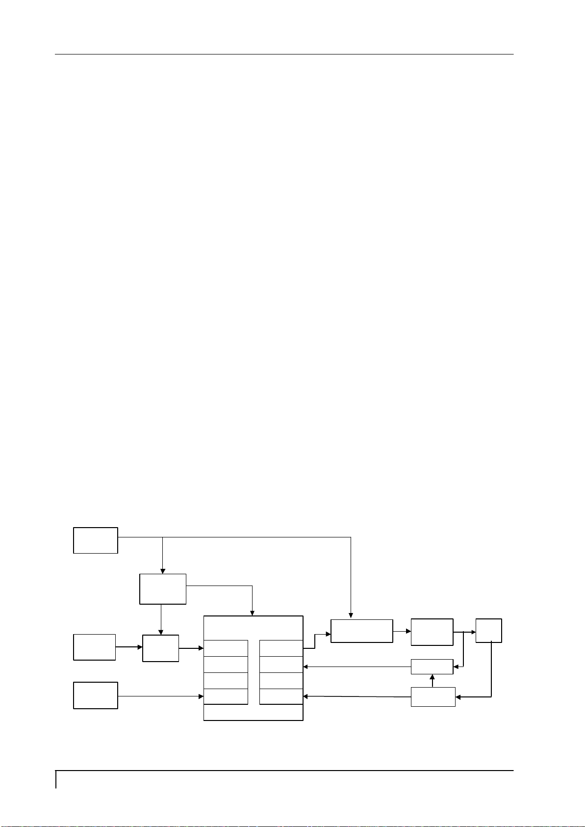
1. Audio circuit (Circuit diagrams Main PWB)
1.1Audioinput
The audiosignalinputreceivedfromthe audioinputterminal(JK011)isappliedtothe amplifierI001of4(L-
CH)and9(R-CH)through the low-pass filterconsisting ofR040,R041,R042,R043,C040 andC041.
Inthisamplifier,controlsofVolumeandmuteareconducted.The audiosignalcontrolledatthe pin6determines
the attenuationofoutputofthe amplifiers.Since then,the signalisoutputtothe jackP003.
1.2Audiooutput
The audiosignalisoutputfromP002outputterminalofthe Audioblocktothe internalspeakersystem.
2. Power supply (Circuit daigrams MAIN PWB)
2.1Line filterconsistsofC801,T801,C802,C803,C804.Iteliminateshigh frequency interference tomeetEMI’s
requirement.
2.2Rec &Filter:
Bridge diodeD801convertsAC source intopulsedDC.ThispulsedDCissmoothedandfilteredbyC805.
R802isan NTC(negative thermalcoefficient)resistor,usedtoreduce inrushcurrenttobewithinsaferange.
2.3Powertransformer:
T802convertsenergy forsquarewave frompowersource C805tosecondarysidetogenerate+12Vand+5V.
2.4Output:
The squarewave fromT802 isrectifiedbyD809,D810,then filteredbyC817,C822 togenerate+12Vand
+5Vrespectively.
2.4.1A5VpowersupplyforLCD module,CPUandlogicisgeneratedfromthe powersource.
2.4.2I308 :3-terminalregulator
A3.3VpowersupplyforI306analogisgeneratedfromthe 5Vsource.
2.4.3I308 :3-terminalregulator
A3.3VpowersupplyforI306digitalisgeneratedfromthe 5Vsource.
Q302,Q303 ON/OFF controlforLCD Module
ON/OFF controlisperformedforpowerON/OFF andalsoforthe powersaving sequence.
2.5Driver:
Q803drive T802fromPWMcontrolofI801 forpowerconverted.
2.6FB:
Negative feedbackCKTconsistsofphotocouplerI802andadjustableregulatorI803.Itcan maintainoutput
voltages+5Vand+12Vatastablelevel.
2.7PWM:
2.7.1Start:When poweristurnedon,Q801 conductsdue tobiasfromC805andR805,R803.C807ischargeda16
voltandastarting currentabout0.3mA topin7ofI801.I801startstooscillateandoutputsapulsetrain
through pin6todrive Q803.
2.7.2OPP :When Q803turnson,C805 suppliesalinearlyincreasing trianglecurrentthrough the primaryinduc
tance ofT802 tothe driverQ803,once the peakvalue ofthiscurrentmultipliedbyR811exceeds1volt, pulse
trainwill beshutdownimmediatelytoprotectQ803,T802frombeing burnedout.
2.7.3Regulation :Ifoutputvoltage +5Vgoesup,the RterminalofI803getsmorebias,accordinglyphototransis
torandphotodiodeflowsmorecurrent. The voltage ofpin2goesuptoo,making the pulsewidthofpin6to
becomenarrower.Sothe outputvoltage +5Vwill bepulleddowntoastablevalue.


 TFT Color User manual")


 TFT Color User manual")