ADTEK UC1 User manual
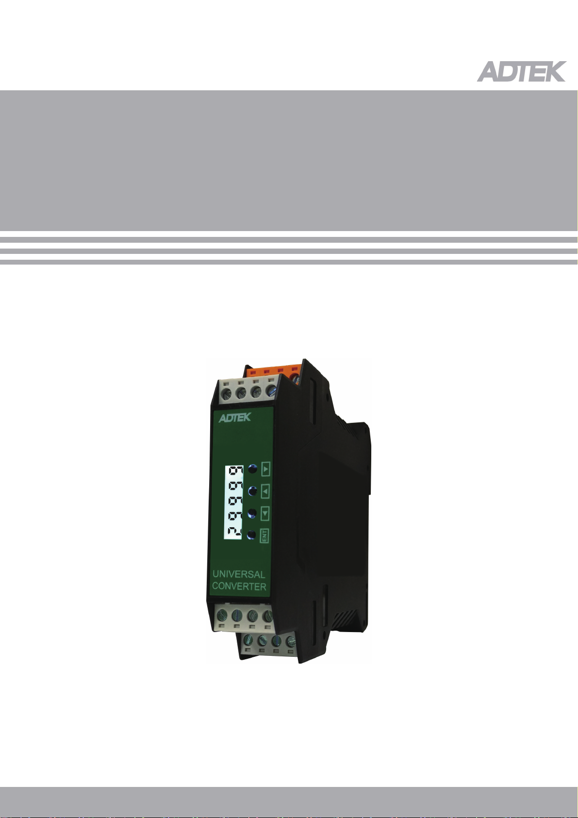
UC1
Manual
Universal Converter
554331-4d-454e-53-41, Rev 1.1
2022-12-05
*554331-4d-454e-53-41*
1
UC1 Manual
UC1 is a universal input converter or isolator which include input signal 0(4)~20mA, 0~10V, Thermocouple,
RTD, etc. Base on measuring signal needed, parameters can be set via panel button with LCD display.
Programmable unit without need of hardware modification or jumper wire/ Dip-Switch.
UC1 offer 3 kind of output option, analogue output or Relay *2 or RS485(Modbus RTU).
With universal input range and different output function, it help reduce product inventory. Parameters can
be easily set via button on site or by software provided through communication port.
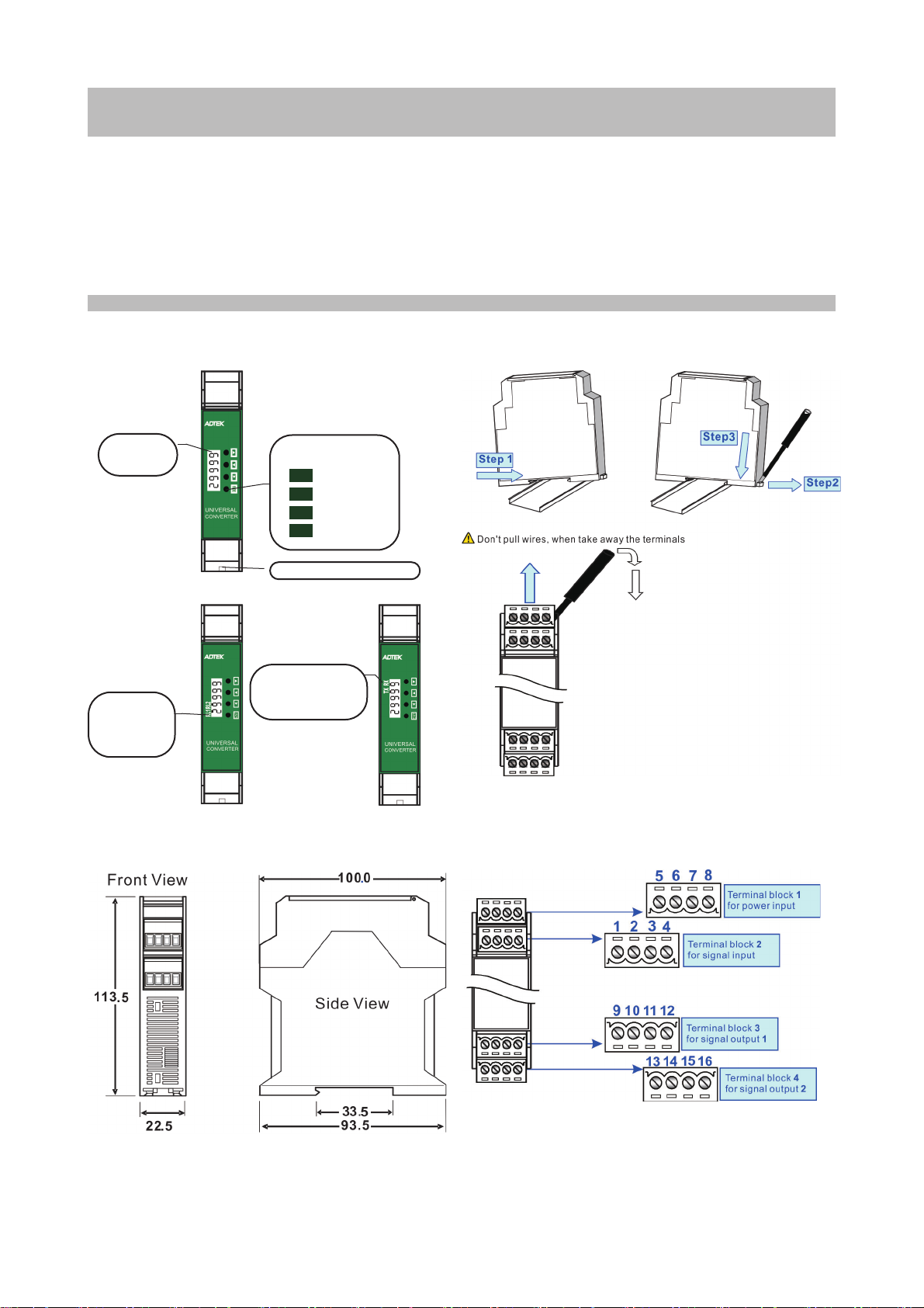
█Top Panel
█Dimensions █Terminal Block
█Installation
Display
screen
Communication
status indication
Communication port
Relay
output
indication
Operation key
Down
Up
Shift
Enter
◄
▼
▲
ENT
2
Key Function Index Setting Status
Enter
(1)In any page, press to access the level.
(2)From the function index, press to access setting
status.
(3)In function index, setting confirmed, save to EEProm.
Shift key
(1)In function index, press for 1 second to return
upper level.
(2)In function group index, press for 1 second to
return measuring page.
(3)In setting status, shift the setting position.
(4)In setting status, press shift key for 1 second to abort
setting and return previous function index.
Up key (1)In function index, press to return to previous
function index.
(2)In setting status for function, select function.
(3)During number setting,press to increase digits.
Down key (1)In function index, press will go to the next function
index page.
(2)In setting status for function, select function.
(3)During number setting, press to decrease digits.
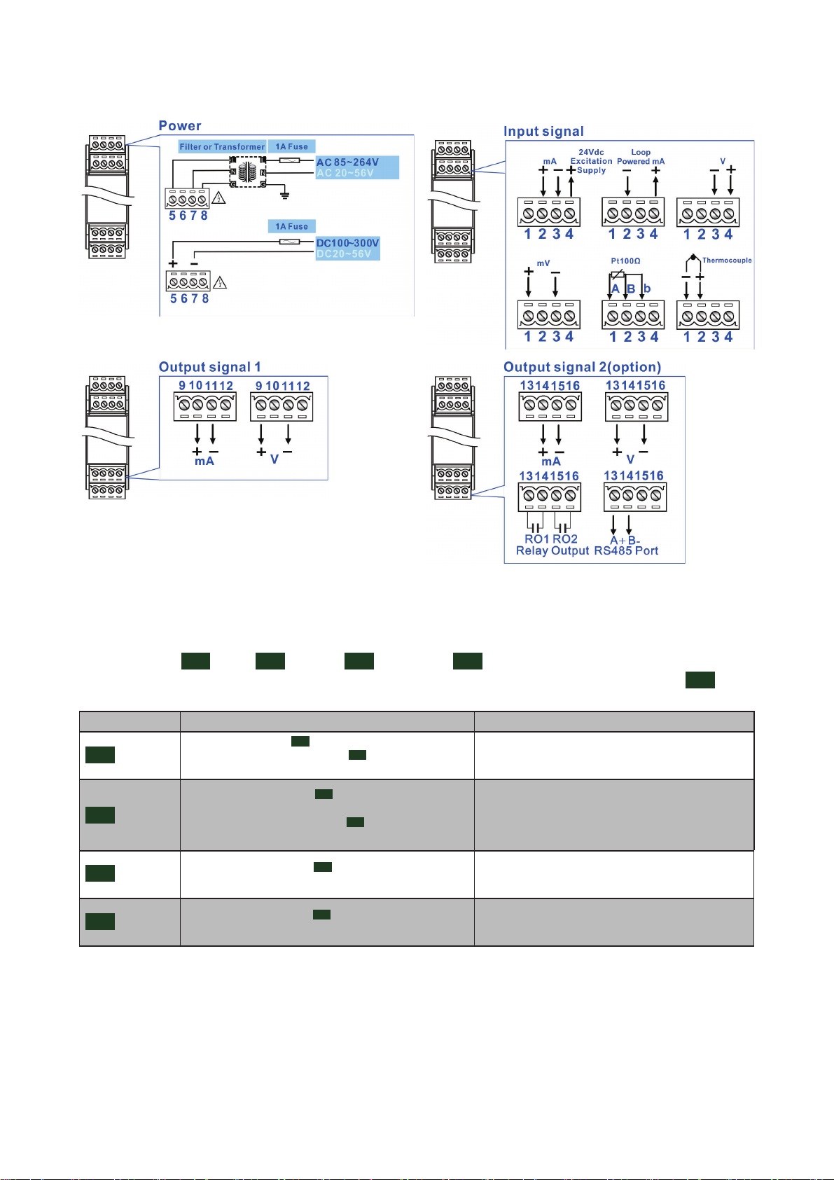
█Connection Diagram
█Operation Key
◄
◄
◄
▼
▼
▲▲
Operating Key:Shift / Up key / Down key / Enter
In Programming Level, the screen will return to Measuring Page after 2 minutes idle, or press for 1
second.
◄
◄
▼▲ ENT
ENT
ENT
ENT

3
█Manual For Setting
Startup screen description and entry parameter setting description
Optional Relay function
Power
Self check
Hold 1 sec
Model Version Input Display value
Display value
Password
Default:1000A-[Input]
C-[Analogue output]
D-[2nd Analogue output]
E-[Relay function]
F-[RS485 function]
→→→→→
→
→
↑
←
←←
↓
↓
↓
↑
↑
8.8.8.8.8 uc1 ver1.0 a0-20 0.0
0.0
pcode
input
ry1.sp
ao
B-[Compensation]
fold
ao2
relay
rs485
ENT
ENT
▼
▼
▼
▲
▲
▲
Correct
Reset relay
→
▼◄ +→
←←
ry2.sp ry.rst
▼ ▼
▲ ▲
NO/YES
R1 set point
energize value
R2 set point
energize value
0~30000 0~30000
0-01 0-02 0-03

4
A-[Input group] V0-10/V0-5/V1-5/
A0-10/A0-20/A4-20/
PT100/TC-K/TC-J/
TC-E/TC-T/TC-N/
TC-R/TC-S/
TC-B/100mV
Type Decimal Low scale High scale
Low cut
Average display value
Average value
Clear zero & Span
adjustment
Moving average
average value
Password
change value
Digital filter
value
Back light
Zero adjustment Span adjustment
→→→→
→→
→→
→→→
←←←
←←
←←
←←←
↓
↓
↓
↑
↑
↑
ai.typ pv.dp lo.sc hi.sc
avg
lo.cut
p.code
m.avgd.filtb.ligh
prog pv.zro pv.spn
z.s.clr
input
▼
▼
▼
▼
▼
▼
▼
▼
▼
▼
▼
▼
▼
▲
▲
▲
▲
▲
▲
▲
▲
▲
▲
▲
▲
▲
A-[Input]Parameters
0/0.0/0.00/
0.000/0.0000
-19999~30000
1~20
0~9999 -19999~30000
0~10
0~15 Minutes
-19999~32767 -19999~32767
NONE/ZERO/
SPAN/BOTH
-19999~30000
1~50
↑
↑
ENT
basic
advnc
A-01 A-02 A-03 A-04
A-05A-06A-07A-08
A-09 A-10 A-11
A-12A-13A-14
↓
↓
↓
↑
↑
↑
▼ ▼
▼▼
▼
▼
▼
▼
▲ ▲
▲▲
▲
▲
▲
▲
↑
B-[Compensation]
B-[Compensation]
fold
Compensation
ON/OFF
Reset all
compensation
value to 0
1st input value
20th present
value
1st present value
20th input value
→→→→
→→
←←←
←←
fd.en fd.rst in1
in20pv20
pv1
in2~19
pv2~19
no/ yesoff/ on 0~30000 0~30000
0~300000~30000
ENT
↑
B-01 B-02 B-03
B-41
B-04
B-05~B-39
B-06~B-40
B-42
5
↓↑
▼
▼▼
▼
▼
▼
▼
▲
▲▲
▲
▲
▲
▲
↑
C-[Analogue output]
ao
Output zero
adjustment
Output span
adjustment
Analogue
output range
Output low
scale
Clear zero and span
Output high
scale
Output low
limit
Output high
limit
→→→→
→→→
←←←
←←←
ao.typ ao.ls ao.hs
ao.zroao.spnao.clr
prog
1.l.lmt
1.h.lmt
-19999~30000V0-10/V0-5/
V1-5/A0-10/
A0-20/A4-20
NONE/ZERO/
SPAN/BOTH
-19999~30000
-19999~32767-19999~32767
0~50%
0~110%
↑
↑
ENT
basic
advnc
▼ ▲
↓↑
C-01 C-02 C-03
C-05
C-04
C-06C-07C-08
C-09
C-[Analogue output]
D-[Optional 2nd Analogue output]
D-[2nd Analogue
output]
ao2
Output zero
adjustment
Output span
adjustment
Type
Range
Output low
scale
Clear zero and
span
Output high
scale
Output low
limit
Output high
limit
→→→→
→→→
←←←
←←←
a2.typ a2.ls a2.hs
a2.zroa2.spna2.clr
prog
2.l.lmt
2.h.lmt
▼ ▲
-19999~30000V0-10/V0-5/
V1-5/A0-10/
A0-20/A4-20
NONE/ZERO/
SPAN/BOTH
-19999~30000
-19999~32767-19999~32767
0~50%
0~110%
↓↑
↑
ENT
▼
▼▼
▼
▼
▼
▲
▲▲
▲
▲
▲
↓↑ ▼▲
↑
advnc
▼
↑
basic
D-01 D-02 D-03
D-05
D-04
D-06D-07D-08
D-09

6
▼ ▲
↓↑
E-[Optional Relay function]
E-[Relay]
relay
R1 hysteresis
Start band Delay time
R1 start delay
R1 DE energized
delay
R2 hysteresis R2 start delay R2 DE energized
delay
R1 mode R2 mode
→→→→
→→
→→→
←←←
←←
←←←
ry.sb ry.sd ry1.md ry2.md
ry1.hyry1.rd prog
advnc
ry2.hy ry2.rd ry2.fd
ry1.fd
0~9:59.90~9999
0~9:59.9
0~9:59.9
0~9999 0~9:59.9 0~9:59.9
OFF/LO/HI/
LO.HLD/
HI.HLD
OFF/LO/HI/
LO.HLD/
HI.HLD
0~9999
↓↑ ▼▲
↑
▲
▲▲
▲
▲
▲
▲
▲
ENT
▼
▼▼
▼
▼
▼
▼
▼
basic
↑
↑
E-01 E-02 E-03 E-04
E-05
E-06E-07E-08
E-09 E-10 E-11
F-[Optional RS485 function]
F-[RS485]
rs485
Address Baud rate Pararity
→→→
←←
adres baud prity
1200/2400/4800/
9600/19200/38400
1~247 N.STB.1/
N.STB.2/
ODD/EVEN
↑
▼ ▼
▲ ▲
ENT F-01 F-02 F-03
7
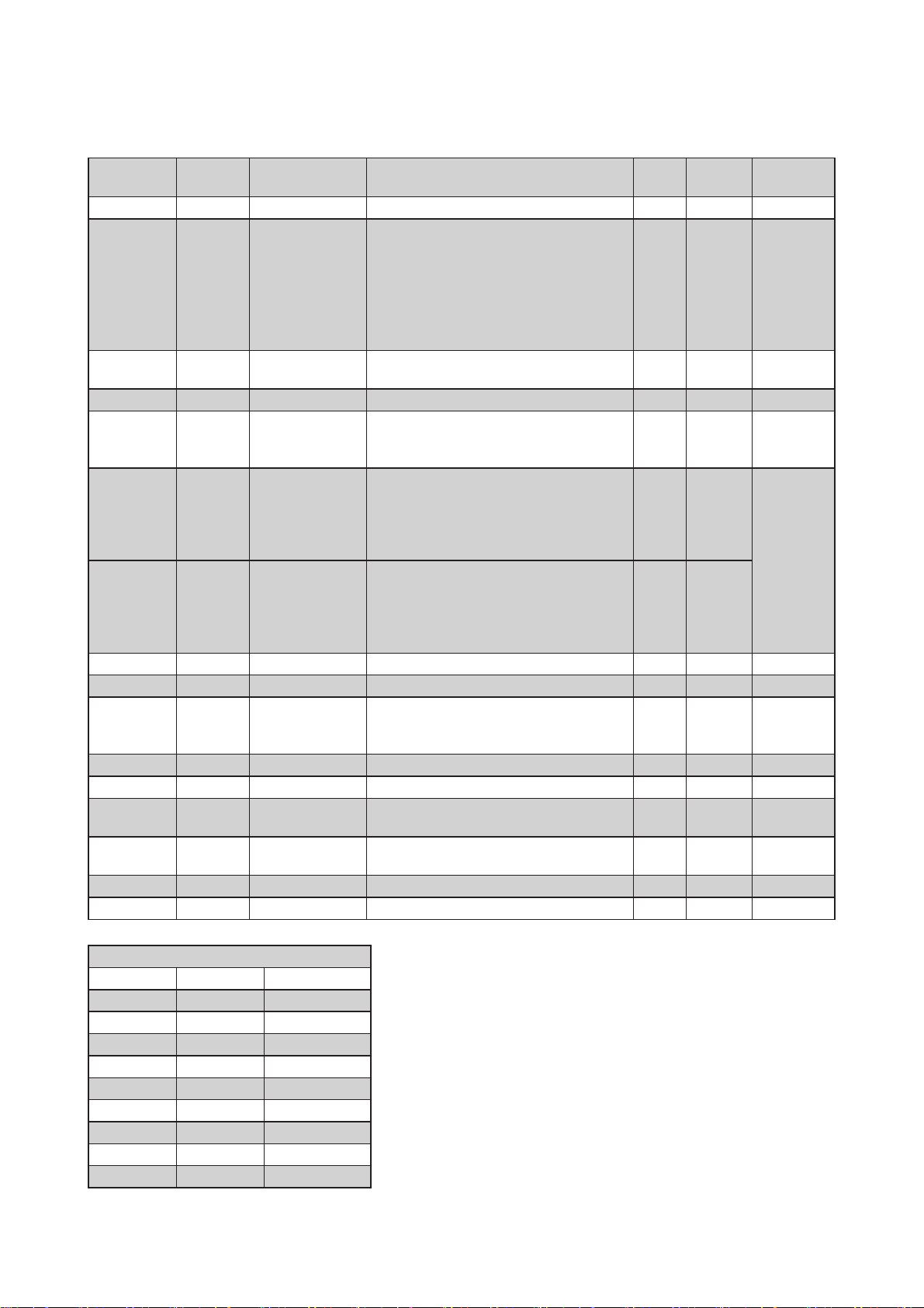
█Address Table(Address in Hexadecimal)
•參數設定階層 (Engineer Level)
Name Address Range Explain Initial Read/
Write Note
PV 0x0000 Present value R
AI.TYP 0x0001 0~15
Type
0: 0-10V 1: 0-5V 2: 1-5V
3: 0-10mA 4: 0-20mA 5: 4-20mA
6: PT100 7: TC-K 8: TC-J
9: TC-E 10: TC-T 11: TC-N
12: TC-R 13: TC-S 14: TC-B
15: 100mV
4 R/W
B.LIGH 0x0002 0~15 Back light
0: always lights unit: minute 1 R/W
Reserved 0x0003 Reserved R/W
PV.DP 0x0004 0~4
Decimal point of setting
0: 0 1: 0.0 2: 0.00 3: 0.000
4: 0.0000
1 R/W
LO.SC 0x0005 -19999~30000 Low scale 0 R/W
When the
input type is
thermocouple
and RTD,
please refer
to the annex 1
for the range
and cannot be
modified.
HI.SC 0x0006 -19999~30000 High scale 30000 R/W
PV.ZRO 0x0007 -19999~32767 Zero adjustment 0 R/W
PV.SPN 0x0008 -19999~32767 span adjustment 0 R/W
Z.S.CLR 0x0009 0~3
Clear zero & Span adjustment
0: NONE 1: ZERO 2: SPAN
3: BOTH
0 R/W
Reserved 0x000A Reserved R/W
LO.CUT 0x000B -19999~30000 Low cut 0 R/W
AVG 0x000C 1~50 Average display value
Average value 5 R/W
M.AVG 0x000D 1~20 Moving average
Average value 1 R/W
P.CODE 0x000E 0~9999 Password change value 1000 R/W
DFILT 0x000F 0~10 Digital filter value 0 R/W
Input Group
Annex 1
LO_SC HI_SC
PT100 -200 850
K -200 1350
J -200 1200
E -200 1000
T -200 400
N -200 1300
R 0 1700
S 0 1750
B 600 1800

8
Relay Group
Name Address Range Explain Initial Read/
Write Note
ST_BAND 0x0014 0~9999 Start band 0 R/W
ST_DELAY 0x0015 0~5999 Delay on (x0.1s) 0 R/W
RELAY1_SP 0x0016 -19999~30000 First relay action function 10000 R/W
RELAY1_MODE 0x0017 0~4
First relay action mode
0: OFF 1: LO 2: HI
3: LO.HOLD 4: HI.HOLD
2 R/W
RELAY1_HY 0x0018 0~9999 First relay hysteresis 0 R/W
RELAY1_RD 0x0019 0~5999 First relay delay on (x0.1s) 0 R/W
RELAY1_FD 0x001A 0~5999 First relay delay off(x0.1s) 0 R/W
RELAY2_SP 0x001B -19999~30000 Secondary relay action function 20000 R/W
RELAY2_MODE 0x001C 0~4
Secondary relay action mode
0: OFF 1: LO 2: HI
3: LO.HOLD 4: HI.HOLD
2 R/W
RELAY2_HY 0x001D 0~9999 Secondary relay hysteresis 0 R/W
RELAY2_RD 0x001E 0~5999 Secondary relay delay on (x0.1s) 0 R/W
RELAY2_FD 0x001F 0~5999 Secondary relay delay off(x0.1s) 0 R/W
Analogue Output Group
Name Address Range Explain Initial Read/
Write Note
AO1.TYP 0x0024 0~5
AO1 Analogue output range
0: 0-10V 1: 0-5V 2: 1-5V
3: 0-10mA 4: 0-20mA 5: 4-20mA
0 R/W
AO1.LS 0x0025 -19999~30000 AO1 Output low scale 0 R/W
AO1.HS 0x0026 -19999~30000 AO1 Output high scale 30000 R/W
AO1_ZERO 0x0027 -19999~32767 AO1 zero adjustment 0 R/W
AO1_SPAN 0x0028 -19999~32767 AO1 span adjustment 0 R/W
AO1.CLR 0x0029 0~3
AO1 Clear zero and span adjustment
0: NONE 1: ZERO
2: SPAN 3: BOTH (Clear all)
0 R/W
AO1.H.LMT 0x002A 0~11000 AO1 Output high limit (x0.01%) 11000 R/W
AO1.L.LMT 0x002B 0~5000 AO1 Output low limit (x0.01%) 0 R/W
AO2.TYP 0x002C 0~5
AO2 Analogue output range
0: 0-10V 1: 0-5V 2: 1-5V
3: 0-10mA 4: 0-20mA 5: 4-20mA
0 R/W
AO2.LS 0x002D -19999~30000 AO2 Output low scale 0 R/W
AO2.HS 0x002E -19999~30000 AO2 Output high scale 30000 R/W
AO2_ZERO 0x002F -19999~32767 AO2 zero adjustment 0 R/W
AO2_SPAN 0x0030 -19999~32767 AO2 span adjustment 0 R/W
AO2.CLR 0x0031 0~3
AO2 Clear zero and span adjustment
0: NONE 1: ZERO
2: SPAN 3: BOTH (Clear all)
0 R/W
AO2.H.LMT 0x003A 0~11000 AO2 Output high limit (x0.01%) 11000 R/W
AO2.L.LMT 0x003B 0~5000 AO2 Output low limit (x0.01%) 0 R/W

9
RS-485 Group
Name Address Range Explain Initial Read/
Write Note
ADRES 0x0032 1~247 Address 1 R/W
BAUD 0x0033 0~5
Baud rate
0: 1200 1: 2400 2: 4800 3: 9600
4: 19200 5: 38400
3 R/W
PRITY 0x0034 0~3
Pararity
0: N,8,1 1: N,8,2
2: O,8,1 3: E,8,1
1 R/W

10
Name Address Range Explain Initial Read/
Write Note
FOLD.EN 0x0041 0~1 Compensation setting ON/OFF
0: OFF 1: ON 0 R/W
FOLD.RST 0x0043 0~1 Reset all compensation value to 0
0: NO 1: YES 0 R/W
FOLD.IN1 0x0044 0~30000 1st input value 0 R/W
FOLD.IN2 0x0045 0~30000 2nd input value 0 R/W
FOLD.IN3 0x0046 0~30000 3rd input value 0 R/W
FOLD.IN4 0x0047 0~30000 4th input value 0 R/W
FOLD.IN5 0x0048 0~30000 5th input value 0 R/W
FOLD.IN6 0x0049 0~30000 6th input value 0 R/W
FOLD.IN7 0x004A 0~30000 7th input value 0 R/W
FOLD.IN8 0x004B 0~30000 8th input value 0 R/W
FOLD.IN9 0x004C 0~30000 9th input value 0 R/W
FOLD.IN10 0x004D 0~30000 10th input value 0 R/W
FOLD.IN11 0x004E 0~30000 11th input value 0 R/W
FOLD.IN12 0x004F 0~30000 12th input value 0 R/W
FOLD.IN13 0x0050 0~30000 13th input value 0 R/W
FOLD.IN14 0x0051 0~30000 14th input value 0 R/W
FOLD.IN15 0x0052 0~30000 15th input value 0 R/W
FOLD.IN16 0x0053 0~30000 16th input value 0 R/W
FOLD.IN17 0x0054 0~30000 17th input value 0 R/W
FOLD.IN18 0x0055 0~30000 18th input value 0 R/W
FOLD.IN19 0x0056 0~30000 19th input value 0 R/W
FOLD.IN20 0x0057 0~30000 20th input value 0 R/W
FOLD.PV1 0x0058 0~30000 1st present value 0 R/W
FOLD.PV2 0x0059 0~30000 2nd present value 0 R/W
FOLD.PV3 0x005A 0~30000 3rd present value 0 R/W
FOLD.PV4 0x005B 0~30000 4th present value 0 R/W
FOLD.PV5 0x005C 0~30000 5th present value 0 R/W
FOLD.PV6 0x005D 0~30000 6th present value 0 R/W
FOLD.PV7 0x005E 0~30000 7th present value 0 R/W
FOLD.PV8 0x005F 0~30000 8th present value 0 R/W
FOLD.PV9 0x0060 0~30000 9th present value 0 R/W
FOLD.PV10 0x0061 0~30000 10th present value 0 R/W
FOLD.PV11 0x0062 0~30000 11th present value 0 R/W
FOLD.PV12 0x0063 0~30000 12th present value 0 R/W
FOLD.PV13 0x0064 0~30000 13th present value 0 R/W
FOLD.PV14 0x0065 0~30000 14th present value 0 R/W
FOLD.PV15 0x0066 0~30000 15th present value 0 R/W
FOLD.PV16 0x0067 0~30000 16th present value 0 R/W
FOLD.PV17 0x0068 0~30000 17th present value 0 R/W
FOLD.PV18 0x0069 0~30000 18th present value 0 R/W
FOLD.PV19 0x006A 0~30000 19th present value 0 R/W
FOLD.PV20 0x006B 0~30000 20th present value 0 R/W
Compensation Group
Other manuals for UC1
1
Table of contents
Other ADTEK Media Converter manuals

Popular Media Converter manuals by other brands

Arec
Arec DS-H2U Quick installation guide

Factor Electronics
Factor Electronics V-66-Wi-Fi installation instructions

GRASS VALLEY
GRASS VALLEY ADVC HD FAMILY datasheet

Speaka Professional
Speaka Professional 1230803 operating instructions

Net Optics
Net Optics Gigabit Fiber installation guide

ICP DAS USA
ICP DAS USA tSH-722i quick start


